

Page 1

DATA SH EET
Product specification
File under Integrated Circuits, IC06
December 1990
INTEGRATED CIRCUITS
74HC/HCT153
Dual 4-input multiplexer
For a complete data sheet, please also download:
•The IC06 74HC/HCT/HCU/HCMOS Logic Family Specifications
•The IC06 74HC/HCT/HCU/HCMOS Logic Package Information
•The IC06 74HC/HCT/HCU/HCMOS Logic Package Outlines
Page 2
December 1990 2
Philips Semiconductors Product specification
Dual 4-input multiplexer 74HC/HCT153
FEATURES
• Non-inverting output
• Separate enable for each output
• Common select inputs
• See ‘253” for 3-state version
• Permits multiplexing from n lines to
1 line
• Enable line provided for cascading
(n lines to 1 line)
• Output capability: standard
• ICC category: MSI
GENERAL DESCRIPTION
The 74HC/HCT153 are high-speed
Si-gate CMOS devices and are pin
compatible with low power Schottky
TTL (LSTTL). They are specified in
compliance with JEDEC standard
no. 7A.
The 74HC/HCT153 have two
identical 4-input multiplexers which
select two bits of data from up to four
sources selected by common data
select inputs (S
0
, S1). The two 4-input
multiplexer circuits have individual
active LOW output enable inputs (1E,
2E) which can be used to strobe the
outputs independently. The outputs
(1Y, 2Y) are forced LOW when the
corresponding output enable inputs
are HIGH.
The “153” is the logic implementation
of a 2-pole, 4-position switch, where
the position of the switch is
determined by the logic levels applied
to S0 and S1.
The logic equations for the outputs
are:
1Y = 1E.(1I0.S1.S0+1I1.S1.S0+
+1I2.S1.S0+1I3.S1.S0)
2Y = 2E.(2I0.S1.S0+2I1.S1.S0+
+2I2.S1.S0+2I3.S1.S0)
The “153” can be used to move data
to a common output bus from a group
of registers. The state of the select
inputs would determine the particular
register from which the data came. An
alternative application is a function
generator. The device can generate
two functions or three variables. This
is useful for implementing highly
irregular random logic.
The “153” is similar to the “253” but
has standard outputs.
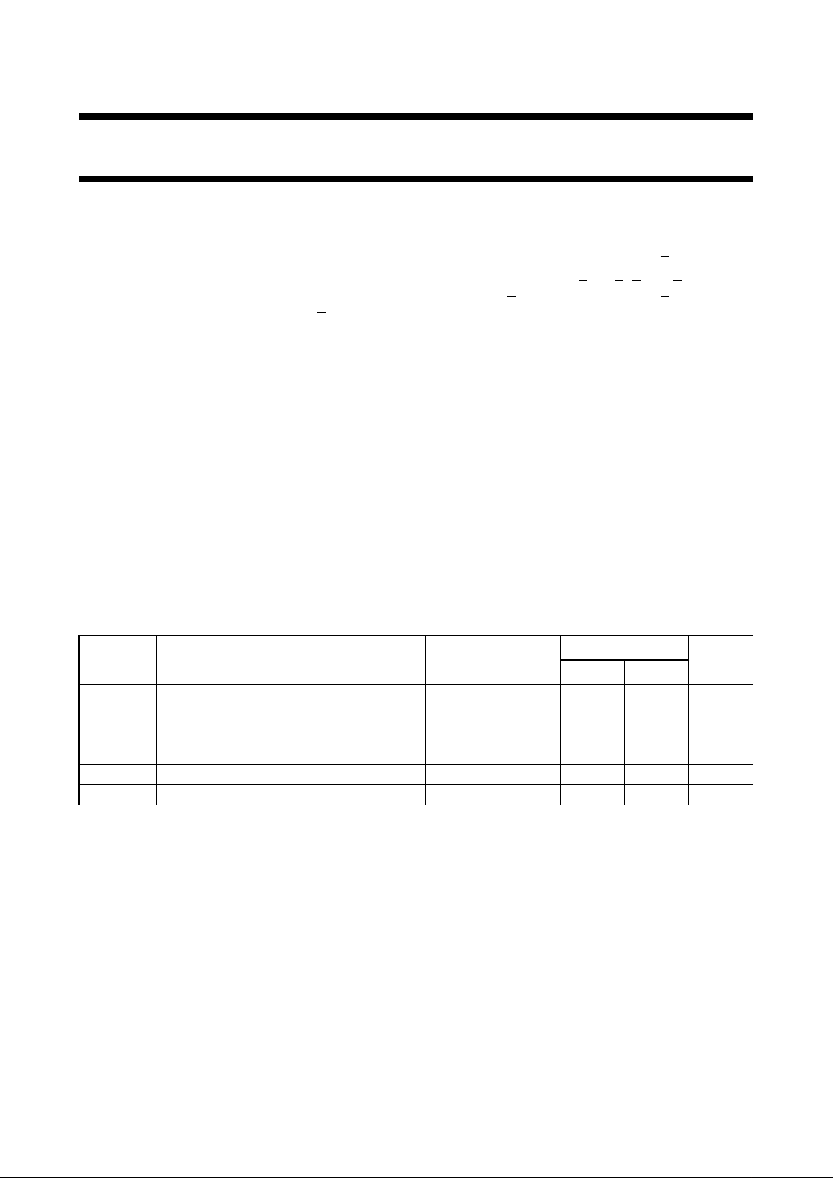
QUICK REFERENCE DATA
GND = 0 V; T
amb
=25°C; tr=tf= 6 ns
SYMBOL PARAMETER CONDITIONS
TYPICAL
UNIT
HC HCT
t
PHL
/ t
PLH
propagation delay CL= 15 pF; VCC=5 V
1I
n
, 2In to nY 14 16 ns
S
n
to nY 15 17 ns
n
E to nY 10 11 ns
C
I
input capacitance 3.5 3.5 pF
C
PD
power dissipation capacitance per multiplexer notes 1 and 2 30 30 pF
Notes
1. CPD is used to determine the dynamic power dissipation (PD in µW):
PD=CPD× V
CC
2
× fi + ∑ (CL× V
CC
2
× fo) where:
fi= input frequency in MHz
fo= output frequency in MHz
CL= output load capacitance in pF
VCC= supply voltage in V
∑ (CL× V
CC
2
× fo) = sum of outputs
2. For HC the condition is VI= GND to V
CC
For HCT the condition is VI= GND to VCC− 1.5 V
ORDERING INFORMATION
See
“74HC/HCT/HCU/HCMOS Logic
Package Information”
.
Page 3
December 1990 3
Philips Semiconductors Product specification
Dual 4-input multiplexer 74HC/HCT153
PIN DESCRIPTION
PIN NO. SYMBOL NAME AND FUNCTION
1, 15 1
E, 2E output enable inputs (active LOW)
14, 2 S
0
, S
1
common data select inputs
6, 5, 4, 3 1I
0
to 1I
3
data inputs from source 1
7 1Y multiplexer output from source 1
8 GND ground (0 V)
9 2Y multiplexer output from source 2
10, 11, 12, 13 2I
0
to 2I
3
data inputs from source 2
16 V
CC
positive supply voltage
Fig.1 Pin configuration. Fig.2 Logic symbol.
Fig.3 IEC logic symbol. Fig.4 Functional diagram.
Page 4

December 1990 4
Philips Semiconductors Product specification
Dual 4-input multiplexer 74HC/HCT153
FUNCTION TABLE
Note
1. H = HIGH voltage level
L = LOW voltage level
X = don’t care
SELECT
INPUTS
DATA INPUTS
OUTPUT
ENABLE
OUTPUT
S
0
S
1
nI
0
nI
1
nI
2
nI
3
nEnY
XXXXXX H L
L
L
H
H
L
L
L
L
L
H
X
X
X
X
L
H
X
X
X
X
X
X
X
X
L
L
L
L
L
H
L
H
L
L
H
H
H
H
H
H
X
X
X
X
X
X
X
X
L
H
X
X
X
X
L
H
L
L
L
L
L
H
L
H
Fig.5 Logic diagram.
Page 5

December 1990 5
Philips Semiconductors Product specification
Dual 4-input multiplexer 74HC/HCT153
DC CHARACTERISTICS FOR 74HC
For the DC characteristics see
“74HC/HCT/HCU/HCMOS Logic Family Specifications”
.
Output capability: standard
ICC category: MSI
AC CHARACTERISTICS FOR 74HC
GND = 0 V; t
r=tf
= 6 ns; CL= 50 pF
SYMBOL PARAMETER
T
amb
(°C)
UNIT
TEST CONDITIONS
74HC
V
CC
(V)
WAVEFORMS
+25 −40 to+85 −40 to+125
min. typ. max. min. max. min. max.
t
PHL
/ t
PLH
propagation delay
1In to nY;
2In to nY
47
17
14
145
29
25
180
36
31
220
44
38
ns
2.0
4.5
6.0
Fig.6
t
PHL
/ t
PLH
propagation delay
Sn to nY
50
18
14
150
30
26
190
38
33
225
45
38
ns
2.0
4.5
6.0
Fig.7
t
PHL
/ t
PLH
propagation delay
nE to nY
33
12
10
100
20
17
125
25
21
150
30
26
ns
2.0
4.5
6.0
Fig.7
t
THL
/ t
TLH
output transition time
19
7
6
75
15
13
95
19
16
110
22
19
ns
2.0
4.5
6.0
Figs 6 and 7
Page 6

December 1990 6
Philips Semiconductors Product specification
Dual 4-input multiplexer 74HC/HCT153
DC CHARACTERISTICS FOR 74HCT
For the DC characteristics see
“74HC/HCT/HCU/HCMOS Logic Family Specifications”
.
Output capability: standard
ICC category: MSI
Note to HCT types
The value of additional quiescent supply current (∆I
CC
) for a unit load of 1 is given in the family specifications.
To determine ∆ICC per input, multiply this value by the unit load coefficient shown in the table below.
AC CHARACTERISTICS FOR 74HCT
GND = 0 V; t
r=tf
= 6 ns; CL= 50 pF
INPUT UNIT LOAD COEFFICIENT
1In, 2I
n
nE
S
n
0.45
0.60
1.35
SYMBOL PARAMETER
T
amb
(°C)
UNIT
TEST CONDITIONS
74HCT
V
CC
(V)
WAVEFORMS
+25 −40 to+85 −40 to+125
min. typ. max. min. max. min. max.
t
PHL
propagation delay
1In to nY;
2In to nY
19 34 43 51 ns 4.5 Fig.6
t
PLH
propagation delay
1In to nY;
2In to nY
13 24 30 36 ns 4.5 Fig.6
t
PHL
/ t
PLH
propagation delay
Sn to nY
20 34 43 51 ns 4.5 Fig.7
t
PHL
/ t
PLH
propagation delay
nE to nY
14 27 34 41 ns 4.5 Fig.7
t
THL
/ t
TLH
output transition time 7 15 19 22 ns 4.5
Figs 6 and 7
Page 7

December 1990 7
Philips Semiconductors Product specification
Dual 4-input multiplexer 74HC/HCT153
AC WAVEFORMS
PACKAGE OUTLINES
See
“74HC/HCT/HCU/HCMOS Logic Package Outlines”
.
Fig.6 Waveforms showing the input (1In, 2In) to output (1Y, 2Y) propagation delays and the output transition times.
(1) HC : VM= 50%; VI= GND to VCC.
HCT: V
M
= 1.3 V; VI= GND to 3 V.
Fig.7 Waveforms showing the select input (S0, S1) and the output enable input (E) to output (1Y, 2Y)
propagation delays and the output transition times.
(1) HC : VM= 50%; VI= GND to VCC.
HCT: V
M
= 1.3 V; VI= GND to 3 V.
 Loading...