

Page 1

DATA SH EET
Product specification
File under Integrated Circuits, IC06
September 1993
INTEGRATED CIRCUITS
74HC/HCT14
Hex inverting Schmitt trigger
For a complete data sheet, please also download:
•The IC06 74HC/HCT/HCU/HCMOS Logic Family Specifications
•The IC06 74HC/HCT/HCU/HCMOS Logic Package Information
•The IC06 74HC/HCT/HCU/HCMOS Logic Package Outlines
Page 2
September 1993 2
Philips Semiconductors Product specification
Hex inverting Schmitt trigger 74HC/HCT14
FEATURES
• Output capability: standard
• ICC category: SSI
GENERAL DESCRIPTION
The 74HC/HCT14 are high-speed Si-gate CMOS devices and are pin compatible with low power Schottky TTL (LSTTL).
They are specified in compliance with JEDEC standard no. 7A.
The 74HC/HCT14 provide six inverting buffers with Schmitt-trigger action. They are capable of transforming slowly
changing input signals into sharply defined, jitter-free output signals.
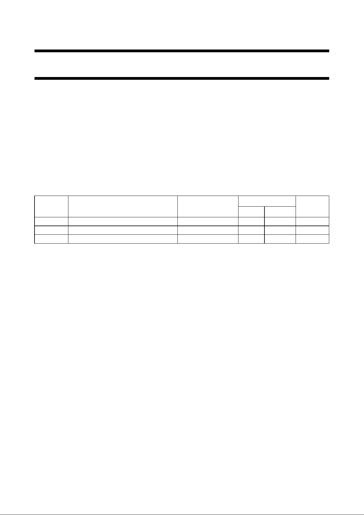
QUICK REFERENCE DATA
GND = 0 V; T
amb
= 25 °C; tr= tf= 6 ns
Notes
1. C
PD
is used to determine the dynamic power dissipation (PDin µW):
PD= CPD× V
CC
2
× fi+ ∑ (CL× V
CC
2
× fo) where:
fi= input frequency in MHz
fo= output frequency in MHz
CL= output load capacitance in pF
VCC= supply voltage in V
∑ (CL× V
CC
2
× fo) = sum of outputs
2. For HC the condition is VI= GND to V
CC
For HCT the condition is VI= GND to VCC− 1.5 V
ORDERING INFORMATION
See
“74HC/HCT/HCU/HCMOS Logic Package Information”
.
SYMBOL PARAMETER CONDITIONS
TYPICAL
UNIT
HC HCT
t
PHL
/ t
PLH
propagation delay nA to nY CL= 15 pF; VCC= 5 V 12 17 ns
C
I
input capacitance 3.5 3.5 pF
C
PD
power dissipation capacitance per gate notes 1 and 2 7 8 pF
Page 3
September 1993 3
Philips Semiconductors Product specification
Hex inverting Schmitt trigger 74HC/HCT14
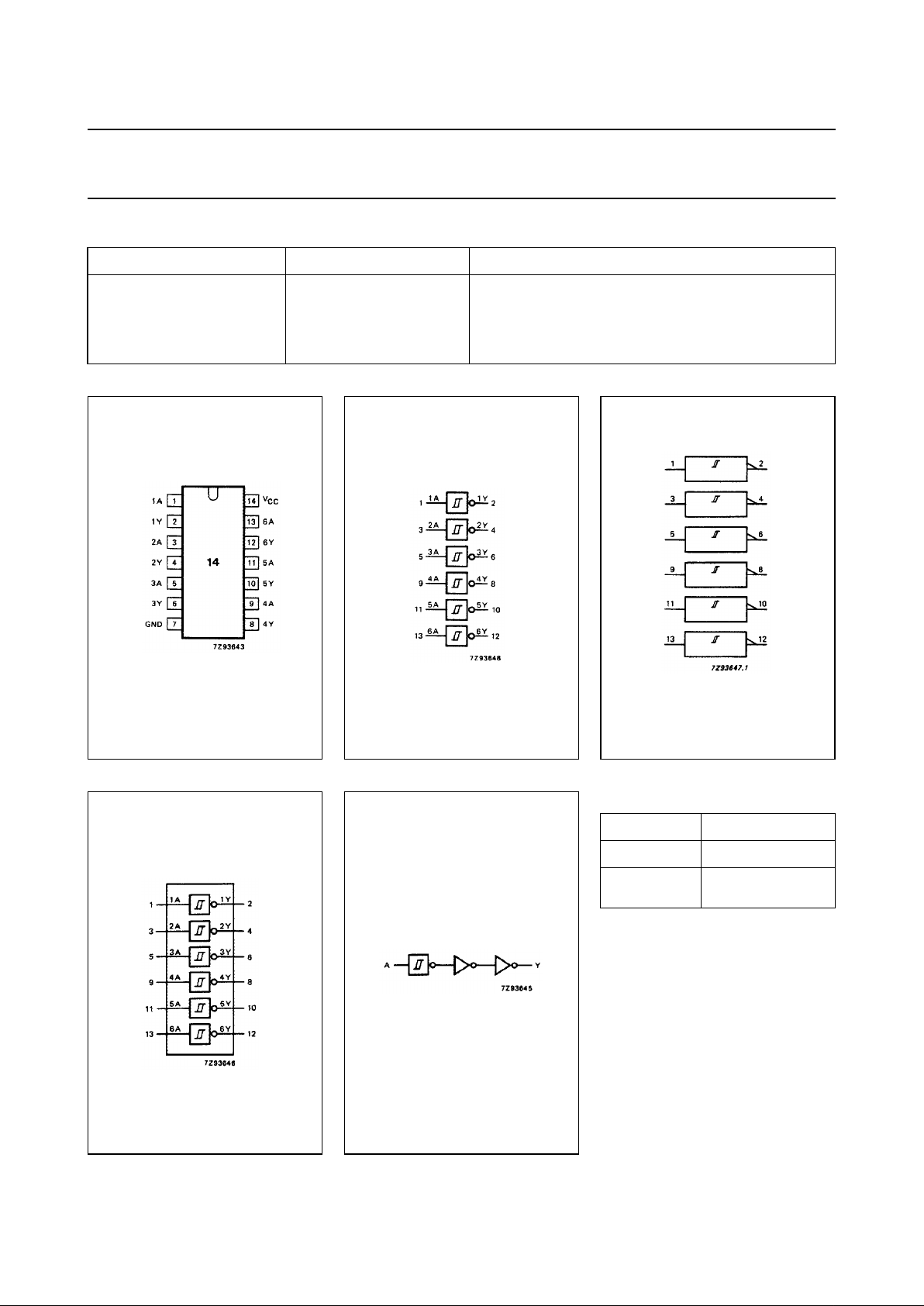
PIN DESCRIPTION
PIN NO. SYMBOL NAME AND FUNCTION
1, 3, 5, 9, 11, 13 1A to 6A data inputs
2, 4, 6, 8, 10, 12 1Y to 6Y data outputs
7 GND ground (0 V)
14 V
CC
positive supply voltage
Fig.1 Pin configuration. Fig.2 Logic symbol. Fig.3 IEC logic symbol.
Fig.4 Functional diagram. Fig.5 Logic diagram
(one Schmitt trigger).
FUNCTION TABLE
Notes
1. H = HIGH voltage level
L = LOW voltage level
APPLICATIONS
• Wave and pulse shapers
• Astable multivibrators
• Monostable multivibrators
INPUT OUTPUT
nA nY
L
H
H
L
Page 4

September 1993 4
Philips Semiconductors Product specification
Hex inverting Schmitt trigger 74HC/HCT14
DC CHARACTERISTICS FOR 74HC
For the DC characteristics see
“74HC/HCT/HCU/HCMOS Logic Family Specifications”
. Transfer characteristics are
given below.
Output capability: standard
ICCcategory: SSI
Transfer characteristics for 74HC
Voltages are referenced to GND (ground = 0 V)
AC CHARACTERISTICS FOR 74HC
GND = 0 V; t
f
= tf= 6 ns; CL= 50 pF
SYMBOL PARAMETER
T
amb
(°C)
UNIT
TEST CONDITIONS
74HC
V
CC
(V)
WAVEFORMS+25 −40 to +85 −40 to +125
min. typ. max. min. max. min. max.
V
T
+ positive-going
threshold
0.7
1.7
2.1
1.18
2.38
3.14
1.5
3.15
4.2
0.7
1.7
2.1
1.5
3.15
4.2
0.7
1.7
2.1
1.5
3.15
4.2
V 2.0
4.5
6.0
Figs 6 and 7
V
T
− negative-going
threshold
0.3
0.9
1.2
0.52
1.40
1.89
0.90
2.00
2.60
0.3
0.90
1.20
0.90
2.00
2.60
0.30
0.90
1.2
0.90
2.00
2.60
V 2.0
4.5
6.0
Figs 6 and 7
V
H
hysteresis
(VT+ − VT−)
0.2
0.4
0.6
0.66
0.98
1.25
1.0
1.4
1.6
0.2
0.4
0.6
1.0
1.4
1.6
0.2
0.4
0.6
1.0
1.4
1.6
V 2.0
4.5
6.0
Figs 6 and 7
SYMBOL PARAMETER
T
amb
(°C)
UNIT
TEST CONDITIONS
74HC
V
CC
(V)
WAVEFORMS+25 −40 to +85 −40 to +125
min. typ. max. min. max. min. max.
t
PHL
/ t
PLH
propagation delay
nA to nY
41
15
12
125
25
21
155
31
26
190
38
32
ns 2.0
4.5
6.0
Fig.8
t
THL
/ t
TLH
output transition
time
19
7
6
75
15
13
95
19
15
110
22
19
ns 2.0
4.5
6.0
Fig.8
Page 5

September 1993 5
Philips Semiconductors Product specification
Hex inverting Schmitt trigger 74HC/HCT14
DC CHARACTERISTICS FOR 74HCT
For the DC characteristics see
“74HC/HCT/HCU/HCMOS Logic Family Specifications”
. Transfer characteristics are
given below.
Output capability: standard
ICCcategory: SSI
Note to HCT types
The value of additional quiescent supply current (∆ICC) for a unit load of 1 is given in the family specifications.
To determine ∆I
CC
per input, multiply this value by the unit load coefficient shown in the table below.
Transfer characteristics for 74HCT
Voltages are referenced to GND (ground = 0 V)
AC CHARACTERISTICS FOR 74HCT
GND = 0 V; t
r
= tf= 6 ns; CL= 50 pF
INPUT UNIT LOAD COEFFICIENT
nA 0.3
SYMBOL PARAMETER
T
amb
(°C)
UNIT
TEST CONDITIONS
74HCT
V
CC
(V)
WAVEFORMS+25 −40 to +85 −40 to +125
min. typ. max. min. max. min. max.
V
T
+ positive-going
threshold
1.2
1.4
1.41
1.59
1.9
2.1
1.2
1.4
1.9
2.1
1.2
1.4
1.9
2.1
V 4.5
5.5
Figs 6 and 7
V
T
− negative-going
threshold
0.5
0.6
0.85
0.99
1.2
1.4
0.5
0.6
1.2
1.4
0.5
0.6
1.2
1.4
V 4.5
5.5
Figs 6 and 7
V
H
hysteresis
(VT+ −VT−)
0.4
0.4
0.56
0.60−−
0.4
0.4−−
0.4
0.4−−
V 4.5
5.5
Figs 6 and 7
SYMBOL PARAMETER
T
amb
(°C)
UNIT
TEST CONDITIONS
74HCT
V
CC
(V)
WAVEFORMS+25 −40 to +85 −40 to +125
min. typ. max. min. max. min. max.
t
PHL
/ t
PLH
propagation delay
nA, to nY
20 34 43 51 ns 4.5 Fig.8
t
THL
/ t
TLH
output transition
time
7 15 19 22 ns 4.5 Fig.8
Page 6

September 1993 6
Philips Semiconductors Product specification
Hex inverting Schmitt trigger 74HC/HCT14
TRANSFER CHARACTERISTIC WAVEFORMS
Fig.6 Transfer characteristic.
Fig.7 Waveforms showing the definition of VT+,
VT− and VH; where VT+ and VT− are
between limits of 20% and 70%.
Fig.8 Typical HC transfer characteristics; VCC= 2 V. Fig.9 Typical HC transfer characteristics; VCC= 4.5 V.
Fig.10 Typical HC transfer characteristics; VCC= 6 V.
Fig.11 Typical HCT transfer characteristics; VCC= 4.5 V.
Page 7

September 1993 7
Philips Semiconductors Product specification
Hex inverting Schmitt trigger 74HC/HCT14
AC WAVEFORMS
Fig.12 Typical HCT transfer characteristics; VCC= 5.5 V.
Fig.13 Waveforms showing the input (nA) to
output (nY) propagation delays and
output transitions times.
(1) HC : VM= 50%; VI= GND to VCC.
HCT: V
M
= 1.3 V; VI= GND to 3 V.
Page 8

September 1993 8
Philips Semiconductors Product specification
Hex inverting Schmitt trigger 74HC/HCT14
APPLICATION INFORMATION
The slow input rise and fall times cause additional power
dissipation, this can be calculated using the following
formula:
Pad= fi× (tr× I
CCa+tf×ICCa
) × VCC.
Where:
Average I
CCa
differs with positive or negative input
transitions, as shown in Figs 14 and 15.
P
ad
= additional power dissipation (µW)
f
i
= input frequency (MHz)
t
r
= input rise time (µs); 10% − 90%
t
f
= input fall time (µs); 10% − 90%
I
CCa
= average additional supply current (µA)
Fig.14 Average ICCfor HC Schmitt trigger devices;
linear change of Vibetween 0.1 VCCto
0.9 V
CC
Fig.15 Average ICCfor HCT Schmitt trigger devices;
linear change of Vibetween 0.1 VCCto
0.9 VCC.
HC/HCT14 used in a relaxation oscillator circuit, see
Fig.16.
Fig.16 Relaxation oscillator using HC/HCT14.
HC : f
1
T
---
1
0.8 RC
------------------ -
≈=
HCT : f
1
T
---
1
0.67 RC
----------------------
≈=
Note to Application information
All values given are typical unless otherwise specified.
PACKAGE OUTLINES
See
“74HC/HCT/HCU/HCMOS Logic Package Outlines”
.
 Loading...