

Page 1
INTEGRATED CIRCUITS
DATA SH EET
For a complete data sheet, please also download:
•The IC06 74HC/HCT/HCU/HCMOS Logic Family Specifications
•The IC06 74HC/HCT/HCU/HCMOS Logic Package Information
•The IC06 74HC/HCT/HCU/HCMOS Logic Package Outlines
74HC/HCT107
Dual JK flip-flop with reset;
negative-edge trigger
Product specification
File under Integrated Circuits, IC06
December 1990
Page 2
Philips Semiconductors Product specification
Dual JK flip-flop with reset; negative-edge trigger 74HC/HCT107
FEATURES
• Output capability: standard
• ICC category: flip-flops
The 74HC/HCT107 are dual negative-edge triggered
JK-type flip-flops featuring individual J, K, clock (n
reset (nR) inputs; also complementary Q and Q outputs.
The J and K inputs must be stable one set-up time prior to
the HIGH-to-LOW clock transition for predictable
GENERAL DESCRIPTION
The 74HC/HCT107 are high-speed Si-gate CMOS devices
and are pin compatible with low power Schottky TTL
(LSTTL). They are specified in compliance with JEDEC
standard no. 7A.
operation.
The reset (nR) is an asynchronous active LOW input.
When LOW, it overrides the clock and data inputs, forcing
the Q output LOW and the Q output HIGH.
Schmitt-trigger action in the clock input makes the circuit
highly tolerant to slower clock rise and fall times.
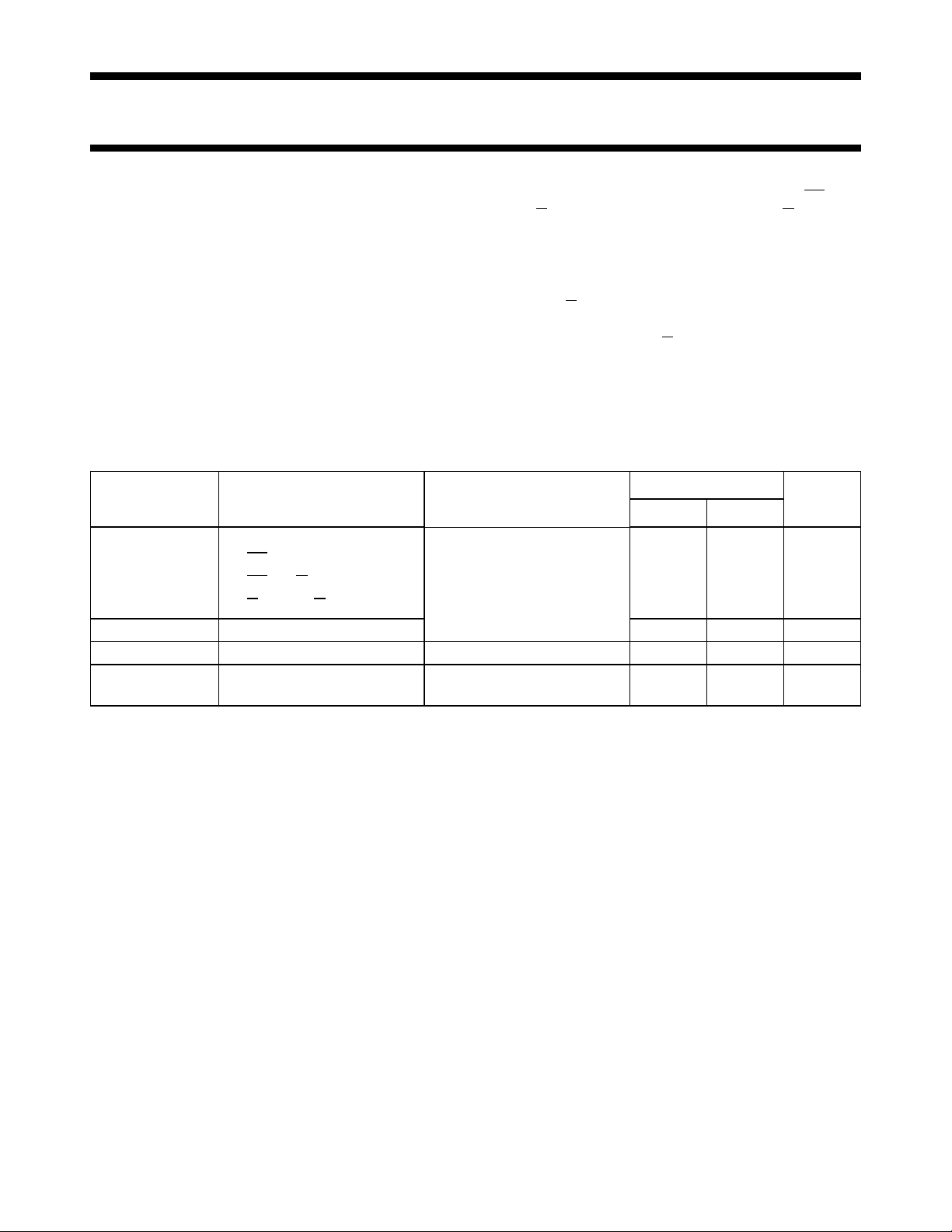
QUICK REFERENCE DATA
GND = 0 V; T
= 25 °C; tr= tf= 6 ns
amb
SYMBOL PARAMETER CONDITIONS
/ t
t
PHL
PLH
f
max
C
I
C
PD
propagation delay
n
CP to nQ 16 16 ns
n
CP to nQ 1618ns
n
R to nQ, nQ 1617ns
CL= 15 pF;
VCC= 5 V
maximum clock frequency 78 73 MHz
input capacitance 3.5 3.5 pF
power dissipation
capacitance per flip-flop
notes 1 and 2 30 30 pF
CP) and
TYPICAL
UNIT
HC HCT
Notes
1. C
is used to determine the dynamic power dissipation (PDin µW):
PD
PD= CPD× V
2
× fi+∑(CL× V
CC
2
× fo) where:
CC
fi= input frequency in MHz
fo= output frequency in MHz
∑ (CL× V
2
× fo) = sum of outputs
CC
CL= output load capacitance in pF
VCC= supply voltage in V
2. For HC the condition is VI= GND to V
CC
For HCT the condition is VI= GND to VCC− 1.5 V.
ORDERING INFORMATION
“74HC/HCT/HCU/HCMOS Logic Package Information”
See
December 1990 2
.
Page 3
Philips Semiconductors Product specification
Dual JK flip-flop with reset; negative-edge trigger 74HC/HCT107
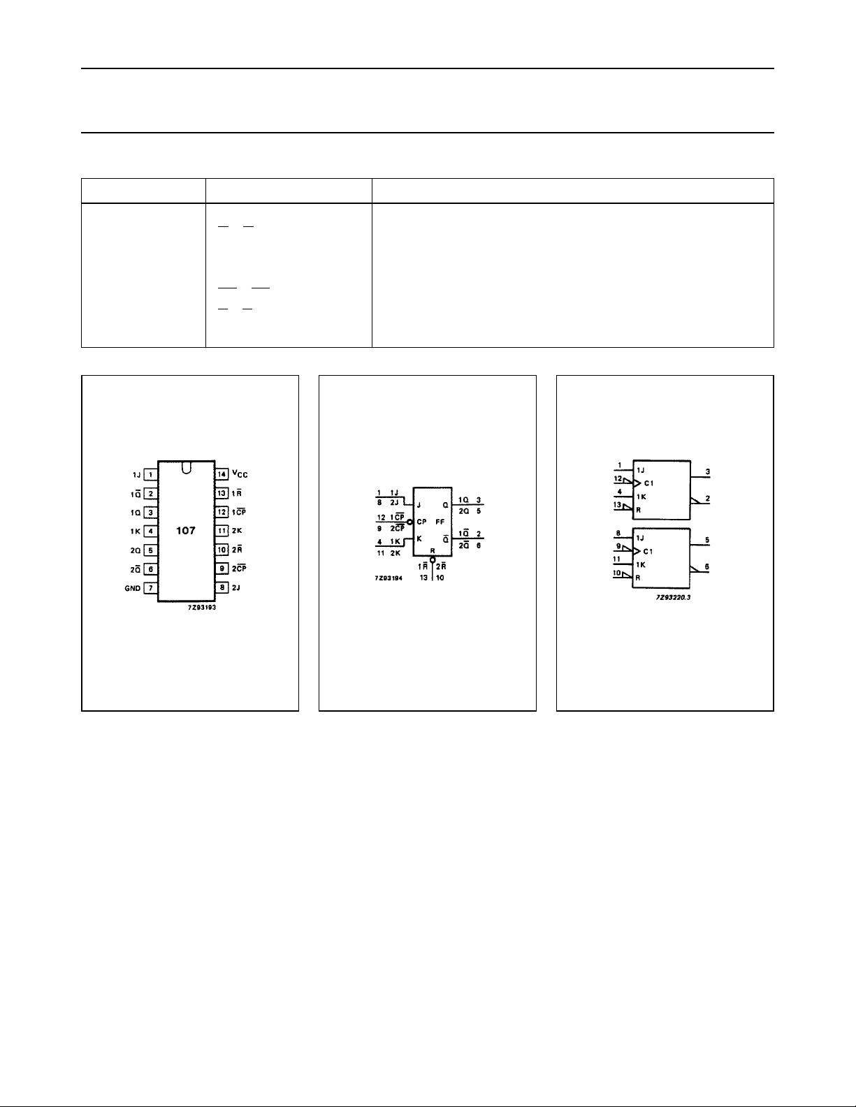
PIN DESCRIPTION
PIN NO. SYMBOL NAME AND FUNCTION
1, 8, 4, 11 1J, 2J, 1K, 2K synchronous inputs; flip-flops 1 and 2
2, 6 1
3, 5 1Q, 2Q true flip-flop outputs
7 GND ground (0 V)
12, 9 1
13, 10 1
14 V
Q, 2Q complement flip-flop outputs
CP, 2CP clock input (HIGH-to-LOW, edge-triggered)
R, 2R asynchronous reset inputs (active LOW)
CC
positive supply voltage
Fig.1 Pin configuration. Fig.2 Logic symbol. Fig.3 IEC logic symbol.
December 1990 3
Page 4
Philips Semiconductors Product specification
Dual JK flip-flop with reset; negative-edge trigger 74HC/HCT107
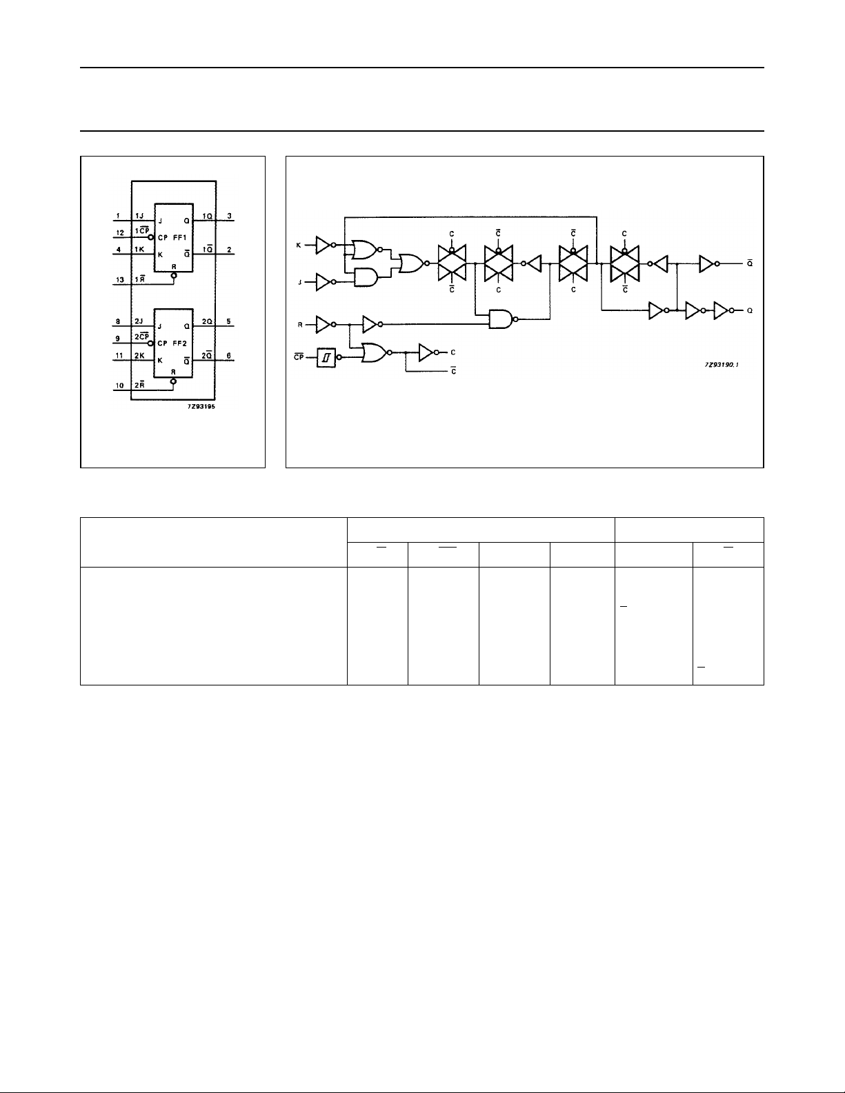
Fig.4 Functional diagram.
FUNCTION TABLE
OPERATING MODE
nRnCP J K Q Q
asynchronous reset L X X X L H
toggle H ↓ hhqq
load “0” (reset) H ↓ IhL H
load “1” (set) H ↓ hIH L
hold “no change” H ↓ IIq
Note
1. H = HIGH voltage level
h = HIGH voltage level one set-up time prior to the HIGH-to-LOW CP transition
L = LOW voltage level
I = LOW voltage level one set-up time prior to the HIGH-to-LOW CP transition
q = lower case letters indicate the state of the referenced output one set-up time prior to the HIGH-to-LOW CP
transition
X = don’t care
↓ = HIGH-to-LOW CP transition
Fig.5 Logic diagram (one flip-flop).
INPUTS OUTPUTS
q
December 1990 4
Page 5
Philips Semiconductors Product specification
Dual JK flip-flop with reset; negative-edge trigger 74HC/HCT107
DC CHARACTERISTICS FOR 74HC
For the DC characteristics see
“74HC/HCT/HCU/HCMOS Logic Family Specifications”
Output capability: standard
ICCcategory: flip-flops
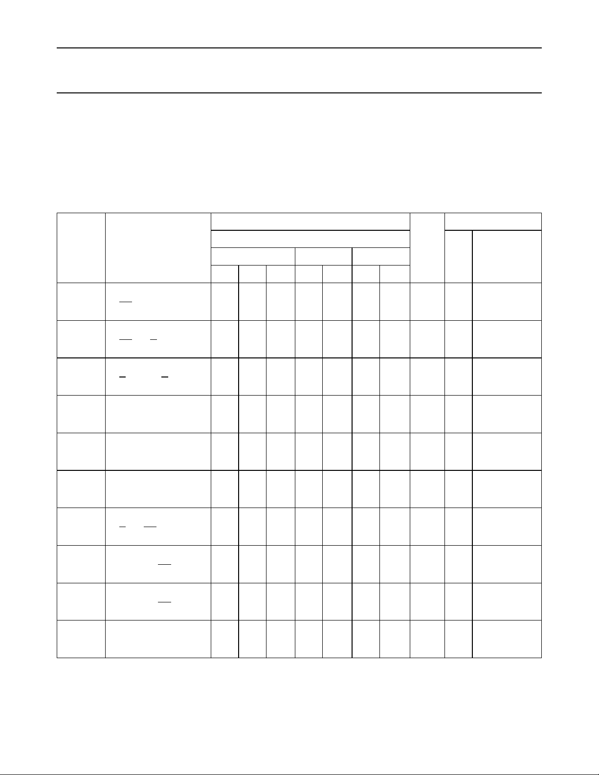
AC CHARACTERISTICS FOR 74HC
GND = 0 V; t
= tf= 6 ns; CL= 50 pF
r
SYMBOL PARAMETER
t
PHL
t
PHL
t
PHL
t
THL
t
W
t
W
t
rem
t
su
t
h
f
max
/ t
/ t
/ t
/ t
propagation delay
PLH
PLH
PLH
TLH
nCP to nQ
propagation delay
nCP to nQ
propagation delay
nR to nQ, nQ
output transition time
clock pulse width
HIGH or LOW
reset pulse width
LOW
removal time
nR to nCP
set-up time
nJ, nK to nCP
hold time
nJ, nK to nCP
maximum clock pulse
frequency
(°C) TEST CONDITIONS
T
amb
74HC
+25 −40 to +85 −40 to +125
min. typ. max. min. max. min. max.
52
80
16
14
80
16
14
60
12
10
100
20
17
3
3
3
6.0
30
35
19
15
52
19
15
52
19
15
19
7
6
22
8
6
22
8
6
19
7
6
22
8
6
−6
−2
−2
23
70
85
160
32
27
160
32
27
155
31
26
75
15
13
100
20
17
100
20
17
75
15
13
125
25
21
3
3
3
4.8
24
28
200
40
34
200
40
34
195
39
33
95
19
16
240
48
41
240
48
41
235
47
40
110
22
19
120
24
20
120
24
20
90
18
15
150
30
26
3
3
3
4.0
20
24
.
ns
ns
ns
ns
ns
ns
ns
ns
ns
MHz
UNIT
V
(V)
2.0
4.5
6.0
2.0
4.5
6.0
2.0
4.5
6.0
2.0
4.5
6.0
2.0
4.5
6.0
2.0
4.5
6.0
2.0
4.5
6.0
2.0
4.5
6.0
2.0
4.5
6.0
2.0
4.5
6.0
CC
WAVEFORMS
Fig.6
Fig.6
Fig.7
Fig.6
Fig.6
Fig.7
Fig.7
Fig.6
Fig.6
Fig.6
December 1990 5
Page 6
Philips Semiconductors Product specification
Dual JK flip-flop with reset; negative-edge trigger 74HC/HCT107
DC CHARACTERISTICS FOR 74HCT
For the DC characteristics see
“74HC/HCT/HCU/HCMOS Logic Family Specifications”
.
Output capability: standard
ICCcategory: flip-flops
Note to HCT types
The value of additional quiescent supply current (∆I
) for a unit load of 1 is given in the family specifications.
CC
To determine ∆ICC per input, multiply this value by the unit load coefficient shown in the table below.
INPUT UNIT LOAD COEFFICIENT
nK
nR
nCP, nJ
0.60
0.65
1.00
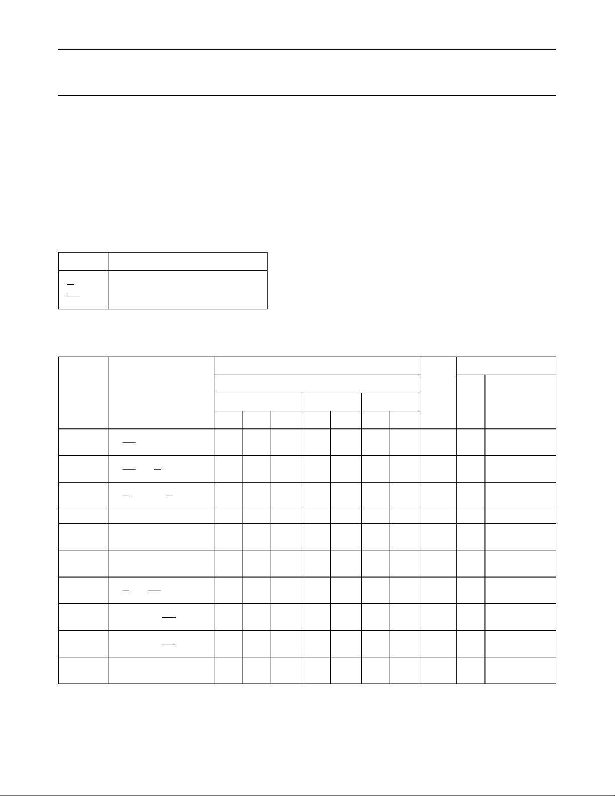
AC CHARACTERISTICS FOR 74HCT
GND = 0 V; t
= tf= 6 ns; CL= 50 pF
f
T
amb
(°C)
TEST CONDITIONS
74HCT
SYMBOL PARAMETER
UNIT
V
(V)
min. typ. max. min. max. min. max.
t
PHL
t
PHL
t
PHL
t
THL
t
W
t
W
t
rem
t
su
t
h
f
max
/ t
/ t
/ t
/ t
propagation delay
PLH
PLH
PLH
TLH
nCP to nQ
propagation delay
nCP to nQ
propagation delay
nR to nQ, nQ
output transition time 7 15 19 22 ns 4.5 Fig.6
clock pulse width
HIGH or LOW
reset pulse width
LOW
removal time
nR to nCP
set-up time
nJ, nK to nCP
hold time
nJ, nK to nCP
maximum clock pulse
frequency
19 36 45 54 ns 4.5 Fig.6
21 36 45 54 ns 4.5 Fig.6
20 38 48 57 ns 4.5 Fig.7
16 9 20 24 ns 4.5 Fig.6
20 11 25 30 ns 4.5 Fig.7
14 8 18 21 ns 4.5 Fig.7
20 7 25 30 ns 4.5 Fig.6
5 −2 5 5 ns 4.5 Fig.6
30 66 24 20 MHz 4.5 Fig.6
CC
WAVEFORMS+25 −40 to +85 −40 to +125
December 1990 6
Page 7
Philips Semiconductors Product specification
Dual JK flip-flop with reset; negative-edge trigger 74HC/HCT107
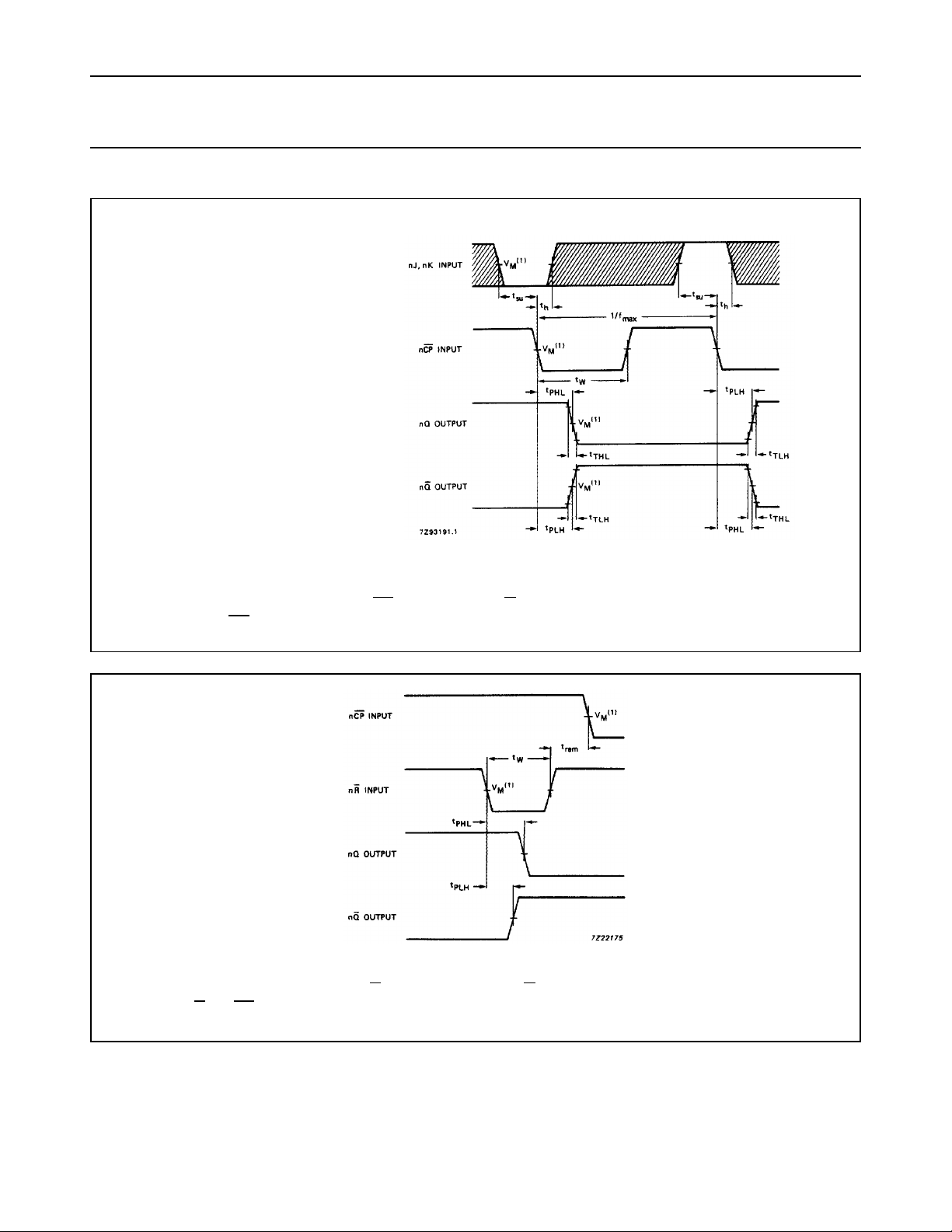
AC WAVEFORMS
The shaded areas indicate when the input is permitted to
change for predictable output performance.
(1) HC : V
= 50%; VI= GND to VCC.
M
= 1.3 V; VI= GND to 3 V.
HCT: V
M
Fig.6 Waveforms showing the clock (nCP) to output (nQ, nQ) propagation delays, the clock pulse width, the J
and K to nCP set-up and hold times, the output transition times and the maximum clock pulse frequency.
(1) HC : VM= 50%; VI= GND to VCC.
= 1.3 V; VI= GND to 3 V.
HCT: V
M
Fig.7 Waveforms showing the reset (nR) input to output (nQ, nQ) propagation delays, the reset pulse width and
the nR to nCP removal time.
PACKAGE OUTLINES
See
“74HC/HCT/HCU/HCMOS Logic Package Outlines”
.
December 1990 7
 Loading...