

Page 1
1/14December 2001
■ HIGH SPEED GTL/GTL + UNIVER SAL
TRANSCEIVER :
t
PD
= 4.6 ns (MAX.) A to B at VCC = 3V
■ COMBINES D-TYPE L ATCHES AND D-T YPE
FLIP-FLOPS FOR OPERATION IN
TRANSPARENT, LATCHED, OR CLOCKED
MODE
■ OPERATING VOLTAGE RANGE:
V
CC
(OPR) = 3.0V to 3.6V
■ SYMMETRICAL OUTPUT IMPEDANCE:
|I
OH
| = IOL=24mA (MIN) at VCC = 3V (A PORT)
■ OUTPUT IMPEDANCE:
I
OL
= 100mA (MIN) at VCC = 3V (B PORT)
■ HIGH-IMPEDANCE ST ATE DURING POWER
UP AND POWER DOWN up to Vcc=1.5V
PERMITT LIVE INSERTION
■ B-PORT PRECHARGED BY BIASVcc
REDUCE NOISE ON THE LINE DURING
LIVE INSERTI O N
■ EDGE RATE-CONTROL INP U T
CONFIGURES THE B-PORT OUTPUT RISE
AND FALL TIMES
■ BUS HOLD ON DATA INPUTS ELIM INATES
THE NEED FOR EXTERNAL PULL-UP/
PULL-DOWN RESISTORS (A PO RT)
■ DISTRIBUTED VCC AND GND PIN
CONFIGURA TI ON MINIMIZES HIGH-SPEED
SWITCHING NOISE IN PARALLEL
COMUNICATIONS .
■ PIN AND FUNCTION COMPATIBLE WITH
74 SERIES 1655
DESCRIPTION
The 74GTL1655 devices are 16-bit high-drive
(100mA), low-output-impedance universal bus
transceivers designed for backplane applications.
The 74GTL1655 devices provide live-insertion
capability for backplane applications by tolerating
active signals on the data ports when the devices
are powered off. In addition, a biasing pin
preconditions the GTL/GTL+ port to minimize
disruption to an active backplane.
The edge rate-control (V
ERC
) input is provided so
the rise and fall time of the B outputs can be
configured to optimize for various backplane
loading conditions. Data flow in each direction is
controlled by output-enable (OEAB
and OEBA),
74GTL1655
16 BIT LVTTL TO GTL/GTL + UNIVERSAL BUS
TRANSCEIVERS WITH LIVE INSERTION
ORDER CODES
PACKAGE TUBE T & R
TSSOP 74GTL1655TTR
TSSOP
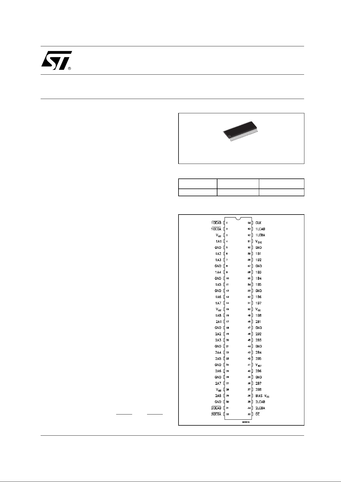
PIN CONNECTION
Page 2

74GTL1655
2/14
latch-enable (LEAB and LEBA), and clock (CLK)
inputs. For A-to-B data flow, the devices operate
in the transparent mode when LEAB is high. When
LEAB is low, the A data is latched if CLK is held at
a high or lo w log ic level. If LEAB is low, the A data
is stored in the latch/flip-flop on the low-to-high
transition of CLK. When OEAB
is low, the outputs
are active. When OEAB
is high, the outputs are in
the high-impedanc e state. Data flow fo r B to A is
similar to that of A to B, but uses OEBA
, LEBA,
and CLK. The output enable (OE
) is used to
disable both ports simultaneously.
Active bus-hold circuitry is provided on the A port
to hold unu sed or floating data inputs at a valid
logic level. When V
CC
is between 0 and 1.5 V, the
device is in the high-impedance state during
power up or power down. Howe ve r, to en sure the
high-impedance st at e a bov e 1.5V , OE
should be
tied to V
CC
through a pullup resistor; the minimum
value of the resistor is determined by the
current-sinking capability of the driver.
All input and output are equipp ed with protection
circuits against static discharge, giving them 2KV
ESD immunity and transient excess voltage .
INPUT AND OUTPUT EQUIVALENT CIRCUIT
PIN DESCRIPTION
PIN N° SYMBOL NAME AND FUNCTION
1, 2 1OEAB
, 1OEBA Output Enable Input
4, 6, 7, 9, 11, 13, 14, 16 1A1 to 1A8 Data Inputs/Outputs LVTTL
17, 19, 20, 22, 23, 25, 27, 29 2A1 to 2A8 Data Inputs/Outputs LVTTL
31, 32 2OEAB
, 2OEBA Output Enable Input
33 OE
Output Enable Input
34, 35 2LEBA, 2LEAB Latch Enable
36 BIAS V
CC
Pre-Charge Supply Voltage
37, 38, 40, 42, 43, 45, 46, 48 2B8 to 2B1 Data Inputs/Outputs GTL/GTL+
41 V
REF
GTL Voltage Reference Input
49, 51, 52, 54, 55, 56, 58, 59 2A1 to 2A8 Data Inputs/Outputs GTL/GTL+
61 V
ERC
Edge Rate Control
62, 63 1LEBA, 1LEAB Latch Enable
64 CLK Clock Input (LOW to HIGH edge triggered)
5, 8, 10, 12, 18, 21, 24, 26, 30,
39, 44, 47, 53, 57, 60
GND Ground (0V)
3, 15, 28, 50 V
CC
Positive Supply Voltage
Page 3
74GTL1655
3/14
FUNCTION TABLE (1)
1) A to B data f l ow is shown. B to A flow is simi l ar, but uses OEBA , LEBA and CLK
2) Outp ut level before the indicated stead y-state inp ut conditions were est ablished, provided that CLK was high before LE AB went low
3) Output level before the indicated steady-state inp ut conditions were estab lis hed
OUTPUT ENABLE TRUTH TABLE
B-PORT EDGE RATE CONTROL (V
ERC
) TRUTH TABLE
INPUTS OUTPUT
MODE
OEAB
LEAB CLK A B
HXXXZIsolation
L H X L L Transparent
L H X H H Transparent
L L L L Registered
L L H H Registered
LLHX
B0
(2)
Previous State
LLLX
B0
(3)
Previous State
INPUTS OUTPUTS
OE
OEAB OEBA A PORT B PORT
L L L Active Active
L L H Z Active
L H L Active Z
LHHZZ
HXXZZ
INPUT V
ERC
OUTPUT B PORT EDGE RATE
LOGIC LEVEL NOMINAL VOLTAGE
H
V
CC
Slow
L GND Fast
Page 4
74GTL1655
4/14
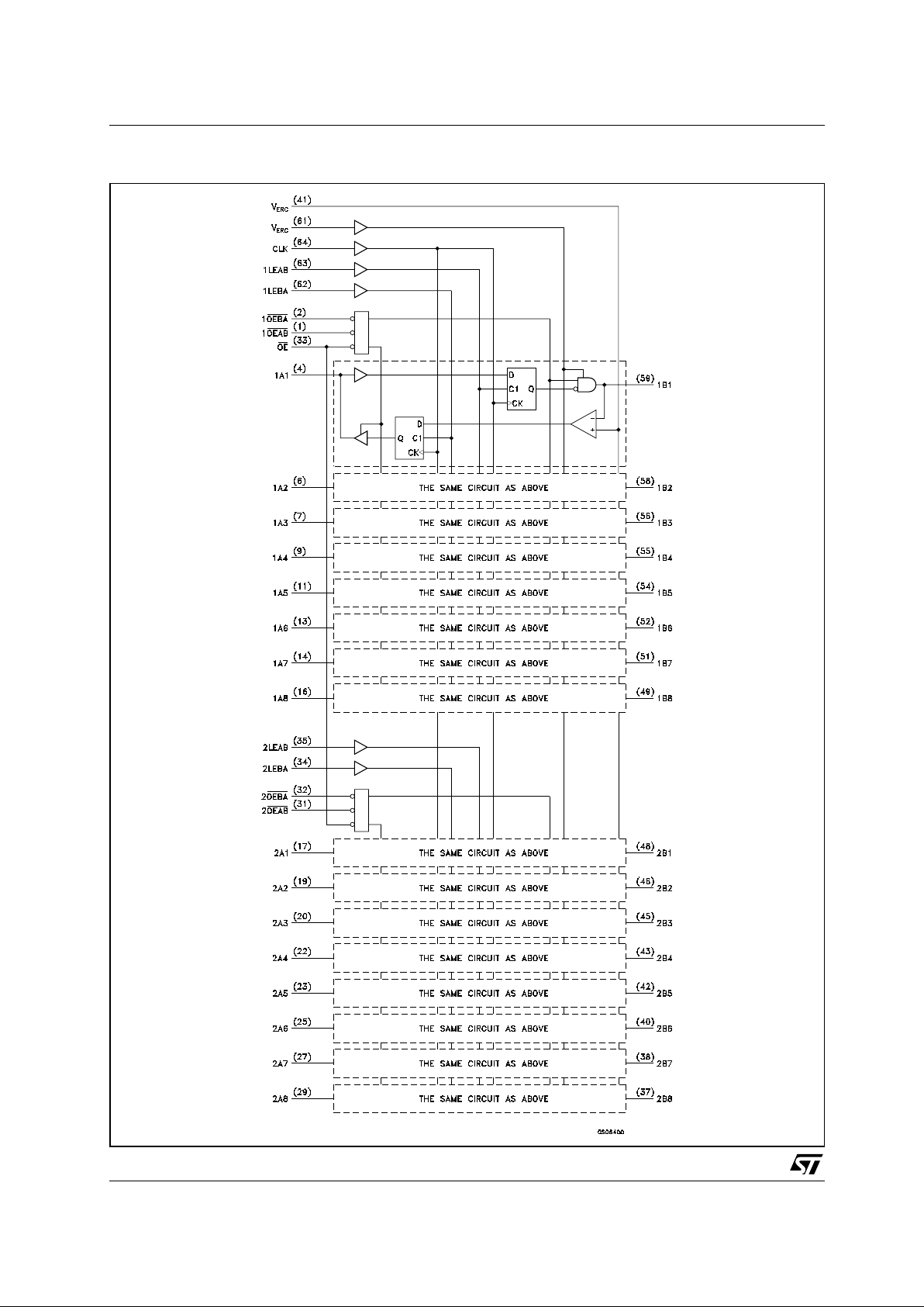
LOGIC DIAGRAM
Page 5

74GTL1655
5/14
ABSOLUTE MAXIMUM RATINGS
Absolute Maximum Rating are those value beyond which damage to the device may occur. Functional operation under these condition is not
implied
RECOMMENDED OPERATING CONDITIONS
1) VTT and RTT can be adjus ted to adapt backplane impedance if DC raccomanded IOL ratings are not exceed ed
2) V
REF
can be adjusted to optimaze noise margin (typ two-thirds VTT)
Symbol Parameter Value Unit
V
CC
Supply Voltage, Bias V
CC
-0.5 to +4.6 V
V
IA
DC Input Voltage A Side, Control Input
-0.5 to +4.6 V
V
IB
DC Input Voltage B Side, V
ERC
, V
REF
-0.5 to +4.6 V
V
OA
DC Output Voltage A Side
-0.5 to +4.6 V
V
OB
DC Output Voltage B Side
-0.5 to +4.6 V
I
IK
DC Input Diode Current
- 50 mA
I
OK
DC Output Diode Current
- 50 mA
I
OA
DC Output Current A Side
± 48 mA
I
OB
DC Output Current B Side in the Low State
200 mA
T
stg
Storage Temperature
-65 to +150 °C
T
L
Lead Temperature (10 sec)
300 °C
Symbol Parameter
Value
Unit
Min. Typ. Max.
V
CC
Supply Voltage
3.0 3.3 3.6 V
V
TT
Termination Voltage GTL 1.14 1.2 1.26
V
GTL+ 1.35 1.5 1.65
V
REF
Supply Voltage GTL 0.74 0.8 0.87
V
GTL+ 0.87 1 1.1
V
I
Input Voltage B port
0
V
TT
V
other
0
V
CC
V
IH
High Level Input Voltage B port V
REF
+0.05
V
other 2
V
IL
Low Level Input Voltage B port V
REF
-0.05
V
other 0.8
I
IK
Input Clamp Current
-18 mA
I
OH
High Level Output Current A port
-24 mA
I
OL
Low Level Output Current A port 24
mA
B port 100
dt/dV
CC
Power -up ramp rate
200 µs/V
T
op
Operating Temperature
-40 85 °C
Page 6

74GTL1655
6/14
DC SPECIFICATIONS
(*) For I/ O ports, the parameter IOZ includes t he input leakage current
Symbol Para mete r
Test Condition Value
Unit
V
CC
(V)
-40 to 85 °C
Min. Typ. Max.
V
IK
High Level Input Voltage
3 -1.2 V
V
OHA
High Level Ouput
Voltage A Port
3 to 3.6
IO=-100µAV
CC
-0.2
V3
I
O
=-12mA
2.4
3
I
O
=-24mA
2.2
V
OLA
Low Level Ouput Voltage
A Port
3 to 3.6
I
O
=100µA
0.2
V3
I
O
=12mA
0.4
3
I
O
=24mA
0.55
V
OLB
Low Level Ouput Voltage
B Port
3
IO=40mA
0.2
V3
I
O
=80mA
0.4
3
I
O
=100mA
0.5
I
I
Input Current Control
3.6
VI = VCC or GND
±10 µA
B Port
3.6
V
I
= VTT or GND
±10 µA
I
off
Power Off Leakage
Current
0V
I
or VO = 0 to 3.6V ±100 µA
I
I(HOLD)
Bus Hold A Port Input
Current
3
V
I
= 0.8V
75 20
µA3
V
I
= 2V
-75
3.6
V
I
= 0 to V
CC
± 500
I
OZHB
3-State Output Current B
Port
3.6 VO = 1.5V 10 µA
I
OZLB
3-State Output Current B
Port
3.6 VO = 0.4V -10 µA
I
OZ
(*) 3-State Output Current A
Port
3.6 VO = VCC or GND ±10 µA
I
OZPU
3-State Output Current A
Port
0 to 1.5 VO = 0.5 to 3V
OE
= LOW
±50 µA
I
OZPD
3-State Output Current A
Port
1.5 to 0 VO = 0.5 to 3V
OE
= LOW
±50 µA
I
CC
Quiescent Supply
Current
3.6 VI = VCC or GND
I
O
=0
10 40 mA
∆I
CC
∆ Supply Current except
B port
3.6
V
IN
= VCC or GND
One input V
CC
=0.6V
1mA
C
I
Control Input
Capacitance
V
IN
= VCC or GND
35pF
C
O
Input Capacitance A Port
V
O
= VCC or GND
56
pF
Input Capacitance B Port 6 8
Page 7

74GTL1655
7/14
LIVE INSERTION SPECIFICATIONS
AC ELECTRICAL CHARACTERISTICS for GTL
(V
CC
=3.3 ± 0.3V, VTT=1.2V, V
REF
=0.8V, V
ERC=VCC
or GND)
Symbol Parameter
Test Condition Value
Unit
V
CC
(V)
-40 to 85 °C
Min. Typ. Max.
I
CC
(Bias
Vcc)
Quiescent Bias Current
0 to 3.0
V
O(Bport)
= 0 to 1.2V 5
mA
3 to 3.6
V
I(Bias Vcc)
= 3 to 3.6V 10
µA
V
O
Output Voltage B Port 0 V
I(Bias Vcc)
= 3.3V 1 1.2 V
I
O
Output Current B Port 0 V
O(Bport)
= 0.4V
V
I(Bias Vcc)
= 3 to 3.6V
-1 µA
0 to 3.6 OE
= 3.3V 100 µA
0 to 1.5 OE
= 0 to 3.3V 100 µA
Symbol Parameter Test Condition
Value
Unit-40 to 85 °C
Min. Typ. Max.
f
MAX
Maximum Frequency
A to B or B to A
160 MHz
t
PLH
Propagation Delay Time
A to B
V
ERC=VCC R1
=12.5Ω CL=30pF
1.5 5.2
ns
t
PHL
1.5 6.2
t
PLH
Propagation Delay Time
CK to B
V
ERC=VCC RL
=12.5Ω CL=30pF
1.5 5.5
ns
t
PHL
1.5 5.8
t
PLH
Propagation Delay Time
LEAB to B
V
ERC=VCC RL
=12.5Ω CL=30pF
1.5 5.8
ns
t
PHL
1.5 6.4
t
EN
Enable Delay Time
OEAB
or OE to B
V
ERC=VCC RL
=12.5Ω CL=30pF 1.5 5.4
ns
t
DIS
Disable Delay Time
OEAB
or OE to B
1.5 6.2
t
PLH
Propagation Delay Time
A to B
V
ERC
=GND RL=12.5Ω CL=30pF
1.5 4.3
ns
t
PHL
1.5 4.6
t
PLH
Propagation Delay Time
CK to B
V
ERC
=GND RL=12.5Ω CL=30pF
1.5 4.3
ns
t
PHL
1.5 4.9
t
PLH
Propagation Delay Time
LEAB to B
V
ERC
=GND RL=12.5Ω CL=30pF
1.5 4.9
ns
t
PHL
1.5 4.8
t
EN
Enable Delay Time
OEAB
or OE to B
V
ERC
=GND RL=12.5Ω CL=30pF 1.5 4.8
ns
t
DIS
Disable Delay Time
OEAB
or OE to B
1.5 4.2
t
PLH
Propagation Delay Time
B to A
RL=500Ω CL=50pF
1.5 4.7
ns
t
PHL
1.5 4.8
t
PLH
Propagation Delay Time
CK to A
RL=500Ω CL=50pF
1.5 4
ns
t
PHL
1.5 4
t
PLH
Propagation Delay Time
LEBA to A
RL=500Ω CL=50pF
1.5 4
ns
t
PHL
1.5 3.7
Page 8

74GTL1655
8/14
AC ELECTRICAL CHARACTERISTICS for GTL+
(V
CC
=3.3 ± 0.3V, VTT=1.5V, V
REF
=1.0V, V
ERC=VCC
or GND)
t
EN
Enable Delay Time
OEBA
or OE to A
R
L
=500Ω R1=500ΩCL=50pF 1 4.6
ns
t
DIS
Disable Delay Time
OEBA
or OE to A
1 6.1
t
SU
Set-up Time Data before clock 2.7
nsData before LE Ck High 2.8
Ck Low 2.6
t
H
Hold Time Data after clock 0.4
ns
Data after LE Ck High or LOW 0.9
t
W
Pulse duration LE High 3
ns
CK High or Low 3
Slew rate Slew rate B output both
transition (0.6 to 1.3V)
V
ERC=VCC
1
ns/V
V
ERC
=GND
1
t
sk
Skew between drivers (in
the same package)
Switching in the same direction 1
ns
Switching in any direction 1
Symbol Parameter Test Condition
Value
Unit-40 to 85 °C
Min. Typ. Max.
f
MAX
Maximum Frequency
B to A or A to B
160 MHz
t
PLH
Propagation Delay Time
A to B
V
ERC=VCC RL
=12.5Ω CL=30pF
1.5 5.1
ns
t
PHL
1.5 6.5
t
PLH
Propagation Delay Time
CK to B
V
ERC=VCC RL
=12.5Ω CL=30pF
1.5 5.4
ns
t
PHL
1.5 6.2
t
PLH
Propagation Delay Time
LEAB to B
V
ERC=VCC RL
=12.5Ω CL=30pF
1.5 5.7
ns
t
PHL
1.5 6.7
t
EN
Enable Delay Time
OEAB
or OE to B
V
ERC=VCC RL
=12.5Ω CL=30pF 1.5 5.5
ns
t
DIS
Disable Delay Time
OEAB
or OE to B
1.5 5.8
t
PLH
Propagation Delay Time
A to B
V
ERC
=GND RL=12.5Ω CL=30pF 1.0
4.3
ns
t
PHL
1.0
4.9
t
PLH
Propagation Delay Time
CK to B
V
ERC
=GND RL=12.5Ω CL=30pF 1.0
4.0
ns
t
PHL
1.0
5.5
t
PLH
Propagation Delay Time
LEAB to B
V
ERC
=GND RL=12.5Ω CL=30pF 1.0
4.0
ns
t
PHL
1.0
5.4
t
EN
Enable Delay Time
OEAB
or OE to B
V
ERC
=GND RL=12.5Ω CL=30pF 1.0 5.1
ns
t
DIS
Disable Delay Time
OEAB
or OE to B
1.0 4.9
Symbol Parameter Test Condition
Value
Unit-40 to 85 °C
Min. Typ. Max.
Page 9

74GTL1655
9/14
t
PLH
Propagation Delay Time
B to A
RL=500Ω CL=50pF
1.5 4.8
ns
t
PHL
1.5 4.7
t
PLH
Propagation Delay Time
CK to A
RL=500Ω CL=50pF
1.5 4.4
ns
t
PHL
1.5 4.1
t
PLH
Propagation Delay Time
LEBA to A
RL=500Ω CL=50pF
1.5 4
ns
t
PHL
1.5 3.7
t
EN
Enable Delay Time
OEBA
or OE to A
R
L
=500Ω R1=500ΩCL=50pF 1 4.2
ns
t
DIS
Disable Delay Time
OEBA
or OE to A
1 6.1
Slew rate Slew rate B output both
transition (0.6 to 1.3V)
V
ERC=VCC RL
=12.5Ω CL=30pF 1
ns/V
V
ERC
=GND RL=12.5Ω CL=30pF
1
t
W
Pulse duration LE High 3
ns
CK High or Low 3
t
SU
Set-up Time Data before clock 2.7
nsData before LE Ck High 2.8
Ck Low 2.6
t
H
Hold Time Data after clock 0.4
ns
Data after LE Ck High or LOW 0.9
t
sk
Skew between drivers (in
the same package)
Switching in the same direction 1
ns
Switching in any direction 1
Symbol Parameter Test Condition
Value
Unit-40 to 85 °C
Min. Typ. Max.
Page 10

74GTL1655
10/14
TEST CIRCUIT FOR "A" OUTPUTS
CL = 50pF or equivalent (in cludes jig and probe capaci tance)
R
L
= R1 = 500Ω or equivalent
R
T
= Z
OUT
of pulse generator (typically 50Ω)
t
r=tf
<=2.5ns
TEST CIRCUIT FOR "B" OUTPUTS
CL = 30pF or equivalent (in cludes jig and probe capaci tance)
R
L
= R1 = 12.5Ω or equivalent
R
T
= Z
OUT
of pulse generator (typically 50Ω)
t
r=tf
<=2.5ns
Test Switch
t
PLH, tPHL
Open
t
PZL, tPLZ
6V
t
PZH, tPHZ
GND
Page 11

74GTL1655
11/14
WAVEFORM 1: PULSE DURATION (A PORT, CONTROL PIN)
WAVEFORM 2: CLOCK TO B PORT PROPAGATION DELAY TIME
WAVEFORM 3: CLOCK TO A PORT PROPAGATION DELAY TIME
Page 12

74GTL1655
12/14
WAVEFORM 4: SETUP AND HOLD TIME
WAVEFORM 4: ENABLE AND DISABLE TIME (A PORT)
Page 13

74GTL1655
13/14
DIM.
mm. inch
MIN. TYP MAX. MIN. TYP. MAX.
A 1.1 0.043
A1 0.05 0.15 0.002 0.006
A2 0.9 0.035
b 0.17 0.27 0.0067 0.011
c 0.09 0.20 0.0035 0.0079
D 16.9 17.1 0.665 0.673
E 8.1 0.318
E1 6.0 6.2 0.236 0.244
e 0.5 BSC 0.0197 BSC
K0° 8°0° 8°
L 0 .50 0.75 0.020 0.030
TSSOP64 MECHANICAL DATA
c
E
b
A2
A
E1
D
1
PIN 1 IDENTIFICATION
A1
L
K
e
7187824A
Page 14

74GTL1655
14/14
Information furnished is believed to be accurate and reliable. However, STMicroelectronics assumes no responsibility f or t he
consequences of use of such informatio n nor for any infringement of paten ts or o ther rig hts of t hird part ies which ma y result from
its use. No license is granted by implication or otherwise under any patent or patent rights of STMicroelectronics. Specifications
mentioned in this publication are subject to change without notice. This publication supersedes and replaces all information
previousl y suppl ied. STM icroel ectronics produc ts are not auth orized for use as c ritica l compone nts in l ife s upport dev ices or
systems without express written approval of STMicroelectronics.
© The ST logo is a registered trademark of STMicroelectronics
© 2001 STMicroelectronics - Printed in Italy - All Rights Reserved
STMicroelectronics GROUP OF COMPANIES
Australia - Brazil - Canada - China - Finland - France - Germany - Hong Kong - India - Israel - Italy - Japan - Malaysia - Malta - Morocco
Singapore - Spain - Sweden - Switzerland - United Kingdom - United States.
© http://www.st.com
 Loading...