

Datasheet 74FR9245SPC, 74FR9245SCX, 74FR9245SC, 74FR9245MSAX, 74FR9245MSA Datasheet (Fairchild Semiconductor)
Page 1
© 1999 Fairchild Semiconductor Corporation DS010914 www.fairchildsemi.com
April 1991
Revised August 1999
74FR9245 9-Bit Bidirectional Transceiver with 3-STATE Outputs
74FR9245
9-Bit Bidirectional Transceiver with 3-STATE Outputs
General Description
The 74FR9245 contains nine non-inverting bidirectional
buffers with 3-STATE outputs and is intended for bu s-oriented applications. Current sinking capability is 64 mA on
both the A and B Ports. The Transmit/Receive (T /R
) input
determines the directio n of data flow through the b idirectional transceiver. Transmit (active-HIGH) enables data
from A Ports to B Ports; Receive (active-LOW) enables
data from B Ports to A Ports. The Output Enable input,
when HIGH, disables both A and B P orts by placi ng them
in a High Z condition.
Features
■ Non-inverting buffers
■ Bidirectional data path
■ A and B output sink capability of 64 mA, source
capability of 15 mA
■ Guaranteed pin-to-pin skew, multiple output switching
and 250 pf delay
Ordering Code:
Devices also availab le in Tape and Reel. Specify by appending th e s uffix let t er “X” to the ordering code.
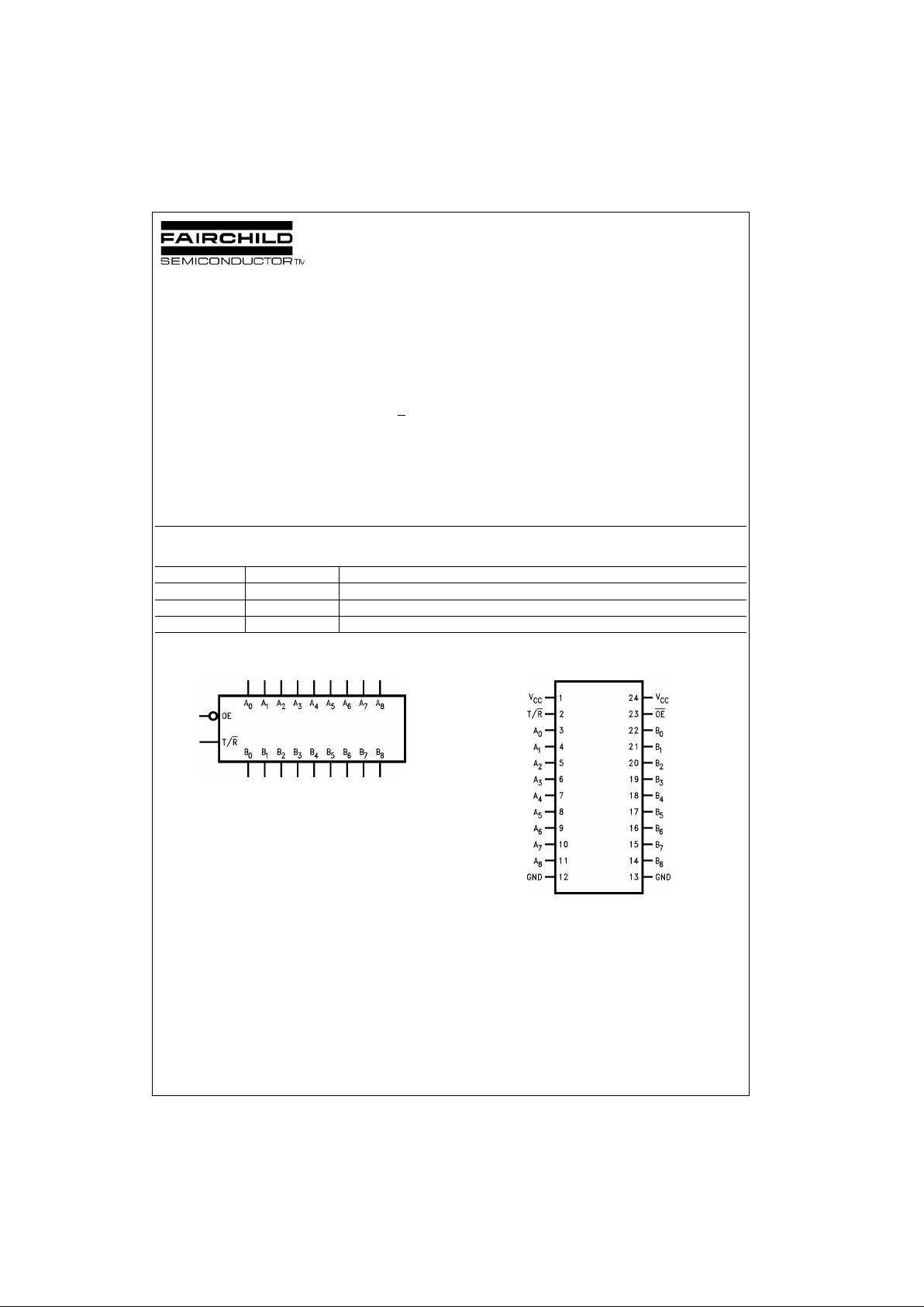
Logic Symbol Connection Diagram
Order Number Package Number Package Description
74FR9245SC M24B 24-Lead Small Outline Integrated Circuit (SOIC), JEDEC MS-013, 0.300 Wide
74FR9245MSA MSA24 24-Lead Shrink Small Outline Package (SSOP), EIAJ TYPE II, 5.3mm Wide
74FR9245SPC N24C 24-Lead Plastic Dual-In-Line Package (PDIP), JEDEC MS-100, 0.300 Wide
Page 2
www.fairchildsemi.com 2
74FR9245
Pin Descriptions Tr uth Table
H = HIGH Voltage Level
L = LOW Voltage Level
X = Immaterial
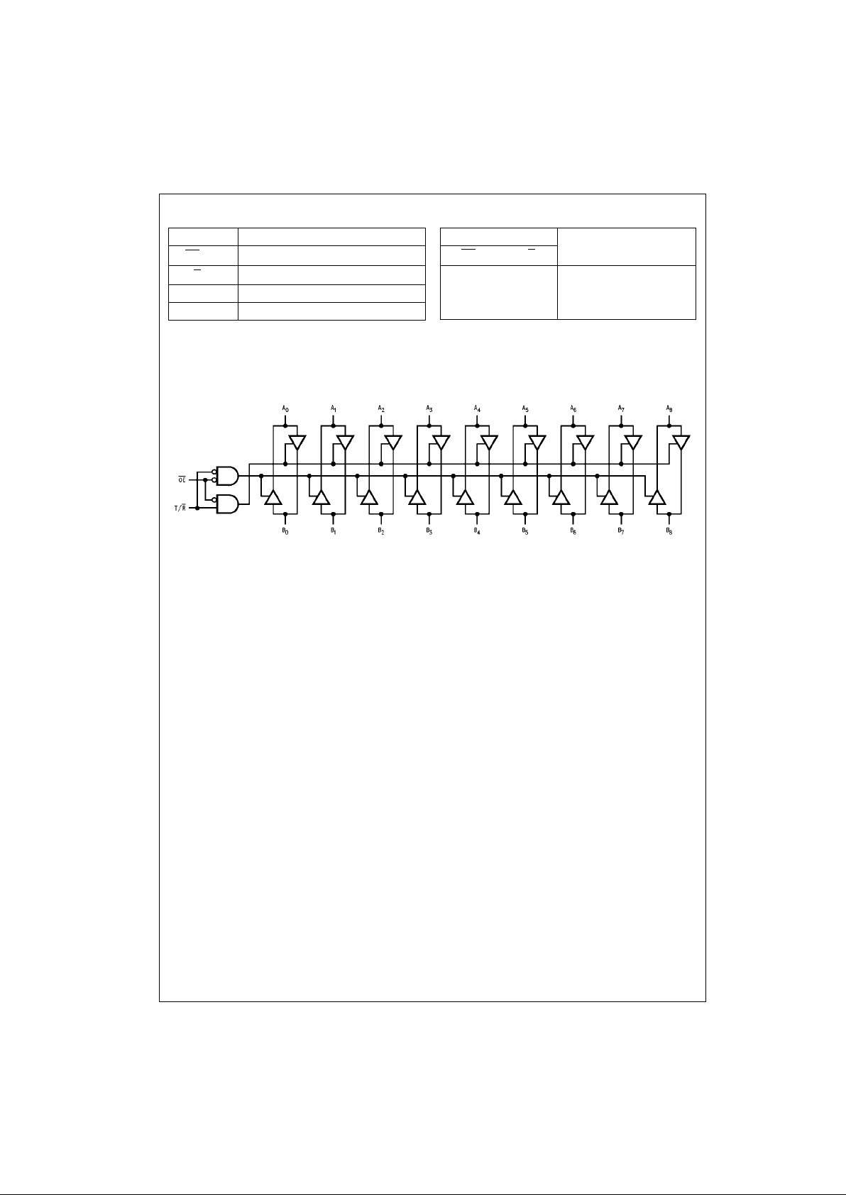
Logic Diagram
Pin Names Description
OE
Output Enable Input (Active-LOW)
T/R
Transmit/Receive Input
A
0–A8
Side A Inputs or 3-STATE Outputs
B
0–B8
Side B Inputs or 3-STATE Outputs
Inputs Output
OE
T/R
L L Bus B Data to Bus A
L H Bus A Data to Bus B
H X High Z State
Page 3

3 www.fairchildsemi.com
74FR9245
Absolute Maximum Ratings(Note 1) Recommended Operating
Conditions
Note 1: Absolute maximum rat ings are value beyond which the device may
be damaged or ha ve its useful life impair ed. Functional opera tion under
these conditions is not im plied.
Note 2: Either voltage limit or curren t limit is sufficient to protect in puts.
DC Electrical Characteristics
Storage Temperature −65°C to +150°C
Ambient Temperature under Bias −55°C to +125°C
Junction Temperature under Bias −55°C to +150°C
V
CC
Pin Potential to Ground Pin −0.5V to +7.0V
Input Voltage (Note 2) −0.5V to +7.0V
Input Current (Note 2) −30 mA to +5.0 mA
Voltage Applied to Output
in HIGH State (with V
CC
= 0V)
Standard Output −0.5V to V
CC
3-STATE Output −0.5V to +5.5V
Current Applied to Output
in LOW State (Max) twic e the rat ed I
OL
(mA)
ESD Last Passing Voltage (Min) 4000V
Free Air Ambi ent Temperature 0°C to +70°C
Supply Voltage +4.5V to +5.5V
Symbol Parameter Min Typ Max Units
V
CC
Conditions
V
IH
Input HIGH Voltage 2.0 V Recognized HIGH Signal
V
IL
Input LOW Voltage 0.8 V Recognized LOW Signal
V
CD
Input Clamp Diode Voltage −1.2 V Min IIN = −18 mA
V
OH
Output HIGH Voltage 2.4 V Min IOH = −3 mA (An, Bn)
2.0 V Min IOH = −15 mA (An, Bn)
V
OL
Output LOW Voltage 0.55 V Min IOL = 64 mA (An, Bn)
I
IH
Input HIGH Current 5 µAMax
VIN = 2.7V (OE, T/R)
I
BVI
Input HIGH Current
7 µAMaxVIN = 7.0V (OE, T/R)
Breakdown Test
I
BVIT
Input HIGH Current
100 µAMaxVIN = 5.5V (An, Bn)
Breakdown Test (I/O)
I
IL
Input LOW Current −250 µAMax
VIN = 0.5V (OE, T/R)
V
ID
Input Leakage Test 4.75 V 0.0 IID = 1.9 µA
All Other Pins Grounded
I
OD
Output Circuit
3.75 µA0.0
V
IOD
= 150 mV
Leakage Current All Other Pins Grounded
IIH + I
OZH
Output Leakage Current 25 µAMaxV
OUT
= 2.7V (An, Bn)
IIL + I
OZL
Output Leakage Current −150 µAMaxV
OUT
= 0.5V (An, Bn)
I
OS
Output Short-Circuit Current −100 −225 mA Max V
OUT
= 0.0V (An, Bn)
I
CEX
Output HIGH Leakage Current 50 µAMaxV
OUT
= VCC (An, Bn)
I
ZZ
Bus Drainage Test 100 µA0.0V
OUT
= 5.25V (An, Bn)
I
CCH
Power Supply Current 55 80 mA Max All Outputs HIGH
I
CCL
Power Supply Current 75 115 mA Max All Outputs LOW
I
CCZ
Power Supply Current 65 85 mA Max Outputs 3-STATE
C
IN
Input Capacitance 8.0 pF 5.0
OE, T/R
17.0 pF 5.0 An, B
n
Page 4

www.fairchildsemi.com 4
74FR9245
AC Electrical Characteristics
Extended AC Electrical Characteristics
Note 3: This specific ation is guaranteed b ut not t es t ed. The limits apply to propagation delays for all paths described swit ch ing in phase,
i.e., all LOW-to-HIGH , H IG H -t o-LOW, 3-STATE-to-HIGH, etc.
Note 4: These specific ations guarant eed but no t tested. The limits repres ent propaga tion delays wi th 250 pF l oad capacitors in place of the 50 pF load
capacitors in the standard AC load. This s pecification pertains to s ingle output switching only.
Note 5: Skew is defined as the absolute value of t he difference betw een the actual p ropagation delays f or any two outp ut s of the same device. T he specifi-
cation applies to any outputs switching HIGH-to-LOW (t
OSHL
), LOW-to-HIGH (t
OSLH
), or HIGH-to-L OW an d/or LOW -to-H IG H (t
OST
). Specifications guara n-
teed with all outputs switching in phase.
Symbol Parameter
TA = +25°CT
A
= 0°C to +70°C
Units
VCC = +5.0V VCC = +50V
CL = 50 pF CL = 50 pF
Min Typ Max Min Max
t
PLH
Propagation Delay 1.0 2.6 3.9 1.0 3.9
ns
t
PHL
An to Bn or Bn to A
n
1.0 1.7 3.9 1.0 3.9
t
PZH
Output Enable Time 2.7 5.0 6.5 2.7 6.5
ns
t
PZL
2.7 4.3 6.5 2.7 6.5
t
PHZ
Output Disable Time 1.7 3.7 6.0 1.7 6.0
ns
t
PLZ
1.7 3.6 6.0 1.7 6.0
TA = 0°C to +70°CT
A
= 0°C to +70°C
VCC = +50V VCC = +50V
Symbol Parameter
CL = 50 pF CL = 250 pF
Units
Eight Outputs Switching (Note 4)
(Note 3)
Min Max Min Max
t
PLH
Propagation Delay 1.0 5.8 2.2 8.1
ns
t
PHL
An to Bn or Bn to A
n
1.05.82.28.1
t
PZH
Output Enable Time 2.7 8.8
ns
t
PZL
2.7 8.8
t
PHZ
Output Disable Time 1.7 7.0
ns
t
PLZ
1.7 7.0
t
OSHL
Pin-to-Pin Skew
2.0 ns
(Note 5) for HL Transitions
t
OSLH
Pin-to-Pin Skew
1.0 ns
(Note 5) for LH Transitions
t
OST
Pin-to-Pin Skew
3.0 ns
(Note 5) for HL/LH Transitions
Page 5

5 www.fairchildsemi.com
74FR9245
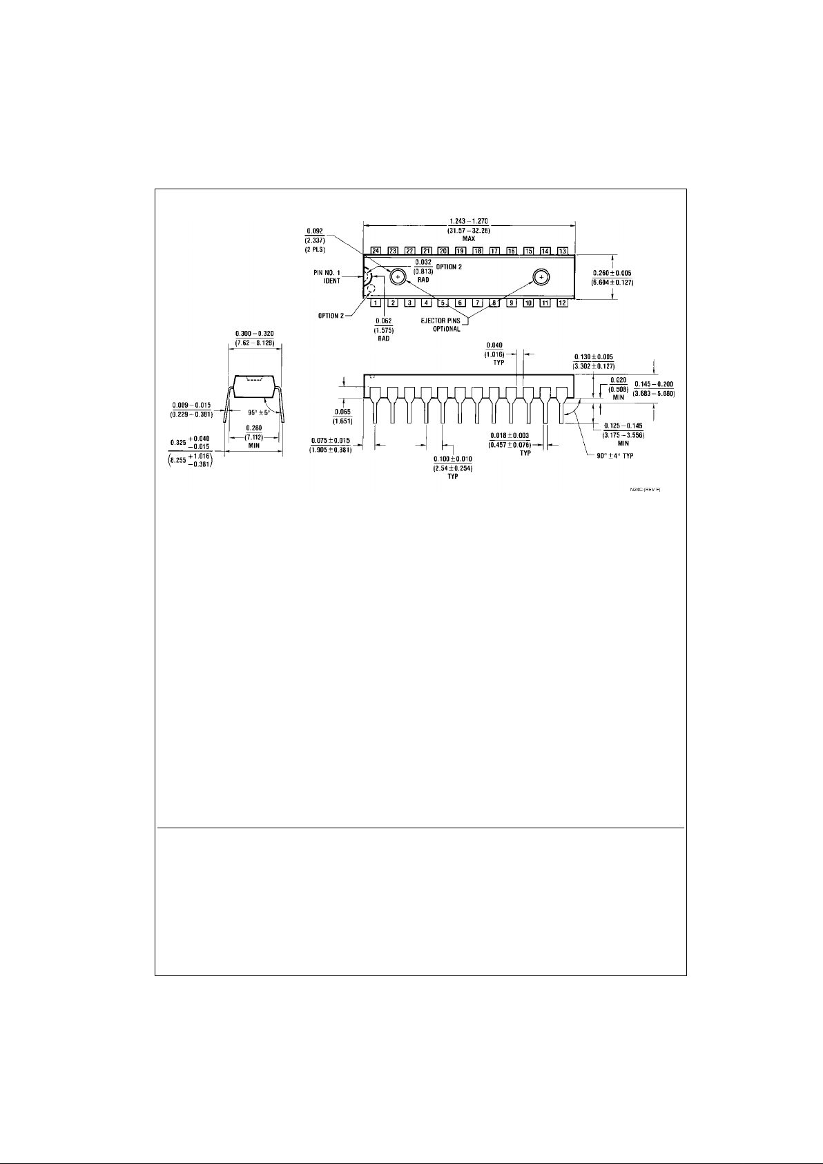
Physical Dimensions inches (millimeters) unless otherwise noted
24-Lead Small Outline Integrated Circuit (SOIC), JEDEC MS-013, 0.300 Wide
Package Number M24B
24-Lead Shrink Small Outline Package (SSOP), EIAJ TYPE II, 5.3mm Wide
Package Number MSA24
Page 6
www.fairchildsemi.com 6
74FR9245 9-Bit Bidirectional Transceiver with 3-STATE Outputs
Physical Dimensions inches (millimeters) unless otherwise noted (Continued)
24-Lead Plastic Dual-In-Line Package (PDIP), JEDEC MS-100, 0.300 Wide
Package Number N24C
Fairchild does not assume any responsibility for use of any circuitry described, no circuit pate nt licenses are implied and
Fairchild reserves the right at any time without notice to change said circuitry and specifications.
LIFE SUPPORT POLICY
FAIRCHILD’S PRODUCTS ARE NOT AUTHORIZED FOR USE AS CRITICAL COMPONENTS IN LIFE SUPPORT
DEVICES OR SYSTEMS WITHOUT THE EXPRESS WRITTEN APPROVAL OF THE PRESIDENT OF FAIRCHILD
SEMICONDUCTOR CORPORATION. As used herein:
1. Life support devices or systems are devices or syste ms
which, (a) are intended for surgical implant into the
body, or (b) support or sustain life, and (c) whose failure
to perform when properly used in accordance with
instructions for use provided in the labeling, can be reasonably expected to result in a significant inju ry to the
user.
2. A critical component i n any compon ent of a lif e support
device or system whose failu re to perform can be reasonably expected to ca use the fa i lure of the life su pp ort
device or system, or to affect its safety or effectiveness.
www.fairchildsemi.com
 Loading...