

Page 1
© 1999 Fairchild Semiconductor Corporation DS010903 www.fairchildsemi.com
January 1991
Revised August 1999
74FR573 Octal D-Type Latch with 3-STATE Outputs
74FR573
Octal D-Type Latch with 3-STATE Outputs
General Description
The 74FR573 is a high speed octal latch with buffered
common Latch Enable (LE) and buffered common Output
Enable (OE
) inputs.
This device is functionally identical to the 74F573.
Features
■ Broadside pinout aids in PC layout
■ Functionally identical to the 74F373, 74F573
■ Outputs have current sourcing capability of 15 mA and
current sinking capability of 64 mA
■ Guarante ed pin-to-pin skew
Ordering Code:
Devices also availab le in Tape and Reel. Specify by appending th e s uffix let t er “X” to the ordering code.
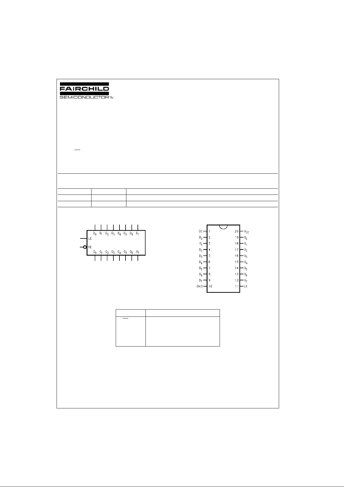
Logic Symbol Connection Diagram
Pin Descriptions
Order Number Package Number Package Description
74FR573SC M20B 20-Lead Small Outline Integrated Circuit (SOIC), JEDEC MS-013, 0.300 Wide
74FR573PC N20A 20-Lead Plastic Dual-In-Line Package (PDIP), JEDEC MS-001, 0.300 Wide
Pin Names Description
OE
Output Enable Input (Active-LOW)
LE Latch Enable Input (Active-HIGH)
D
0–D7
Data Inputs
O
0–O7
3-STATE Latch Outputs
Page 2
www.fairchildsemi.com 2
74FR573
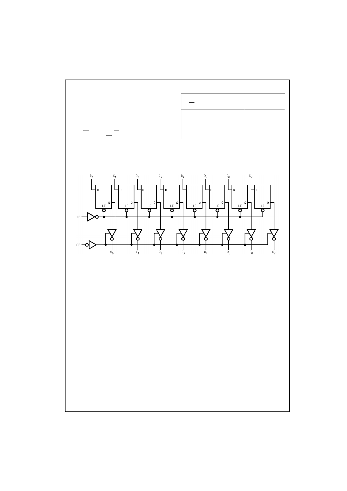
Functional Description
The 74FR573 conta ins eight D-type latches with 3 -STATE
output buffers. When th e latch enable (LE ) input is HIGH,
data on the D
n
inputs enters the latches. In this co ndition
the latches are transparent, i.e., a latch output will chang e
state each time its D input ch anges. Whe n LE is L OW the
latches store the information that was present on th e D
inputs a setup time preceding the HIGH-to-LOW transitio n
of LE. The 3-STATE buffers are controlled by the O utput
Enable (OE
) input. When OE is LOW, the buffers are in the
bi-state mode. When OE
is HIGH the buffers are in the high
impedance mode, but this doe s not interfere with enterin g
new data into the latches.
Function Table
H = HIGH Voltage Level
L = LOW Voltage Level
X = Immaterial
Logic Diagram
Inputs Output
OE
LE D
n
O
n
LHH H
LHL L
LLX O
n − 1
H X X High Z State
Page 3

3 www.fairchildsemi.com
74FR573
Absolute Maximum Ratings(Note 1) Recommended Operating
Conditions
Note 1: Absolute maximum ratings are values beyon d which the device
may be damaged or have its useful life impaired . Functional operation
under these condit ions is not implied.
Note 2: Either voltage limit or curren t limit is sufficient to protect in puts.
DC Electrical Characteristics
Storage Temperature −65°C to +150°C
Ambient Temperature under Bias −55°C to 125°C
Junction Temperature under Bias −55° to +150°C
V
CC
Pin Potential to Ground Pin −0.5V to +7.0V
Input Voltage (Note 2) −0.5V to +7.0V
Input Current (Note 2) −30 mA to +5.0 mA
Voltage Applied to Output
in HIGH State (with V
CC
= 0V)
Standard Output −0.5V to V
CC
3-STATE Output −0.5 to +5.5V
Current Applied to Output
in LOW State (Max) twice the rated I
OL
(mA)
ESD Last Passing Voltage (Min) 4000V
Free Air Ambi ent Temperat ure 0°C to +70°C
Supply Voltage +4.5V to 5.5V
Symbol Parameter Min Typ Max Units
V
CC
Conditions
V
IH
Input HIGH Voltage 2.0 V Recognized HIGH Signal
V
IL
Input LOW Voltage 0.8 V Recognized LOW Signal
V
CD
Input Clamp Diode Voltage −1.2 V Min IIN = −18 mA
V
OH
Output HIGH 2.4 V Min IOH = −3 mA
Voltage 2.0 V Min IOH = −15 mA
V
OL
Output LOW Voltage 0.55 V Min I
IOL
= 64 mA
I
IH
Input HIGH Current 5 µAMaxVIN = 2.7V
I
BVI
Input HIGH Current
7 µAMaxVIN = 7.0V
Breakdown Test
I
IL
Input LOW Current −150 µAMaxVIN = 0.5V Data Inputs
−100 µAMaxVIN = 0.5V Control Inputs
V
ID
Input Leakage Test 4.75 V 0.0 IID = 1.9 µA,
All Other Pins Grounded
I
OD
Output Circuit
3.75 µA0.0
µA
IOD
= 150 mV,
Leakage Current All Other Pins Grounded
I
OZH
Output Leakage Current 20 µAMaxV
OUT
= 2.7V
I
OZL
Output Leakage Current −20 µAMaxV
OUT
= 0.5V
I
OS
Output Short-Circuit Current −100 −225 mA Max V
OUT
= 0.0V
I
CEX
Output HIGH Leakage Current 50 µAMaxV
OUT
= V
CC
I
ZZ
Bus Drainage Test 100 µA0.0V
OUT
= 5.25V
I
CCH
Power Supply Current 26 32 mA Max All Outputs HIGH
I
CCL
Power Supply Current 55 65 mA Max All Outputs LOW
I
CCZ
Power Supply Current 32 40 mA Max Outputs 3-STATED
C
IN
Input Capacitance 8.0 pF 5.0
Page 4

www.fairchildsemi.com 4
74FR573
AC Electrical Characteristics
AC Operating Requirements
Extended AC Electrical Characteristics
Note 3: This specific ation is guaranteed b ut not t es t ed. The limits apply to propagation delays for all paths described swit ch ing in phase,
i.e. all LOW-to-HIGH, HIGH-to-LOW, 3-STATE-to-HIGH, etc.
Note 4: These specific ations guarant eed but no t tested. The limits repres ent propaga tion delays wi th 250 pF l oad capacitors in place of the 50 pF load
capacitors in the standard AC load. This s pecification pertains to s ingle output switching only.
Note 5: Skew is defined as the absolute value of t he difference betw een the actual p ropagation delays f or any two outp ut s of the same device. T he specifi-
cation applies to any outputs s witching HIG H-to-LOW, (t
OSHL
), LOW-to-HIGH, (t
OSLH
) or any combinatio n of HIGH-to -LOW and/or LO W-to-HIGH, ( t
OST
).
Specifications guaranteed with all outputs switching in phase.
Symbol Parameter
TA = +25°CT
A
= 0°C to +70°C
Units
VCC = +5.0V VCC = +5.0V
CL = 50 pF CL = 50 pF
Min Typ Max Min Max
t
PLH
Propagation Delay 1.7 2.9 4.5 1.7 4.5
ns
t
PHL
Dn to O
n
1.7 2.6 4.5 1.7 4.5
t
PLH
Propagation Delay 2.6 6.0 8.5 2.6 8.5
ns
t
PHL
LE to O
n
2.6 4.3 8.5 2.6 8.5
t
PZH
Output Enable Time 2.8 4.0 7.4 2.8 7.4
ns
t
PZL
2.8 5.0 7.4 2.8 7.4
t
PHZ
Output Disable Time 2.2 4.0 6.3 2.2 6.3
ns
t
PLZ
2.2 3.5 6.3 2.2 6.3
Symbol Parameter
TA = +25°CT
A
= 0°C to +70°C
Units
VCC = +5.0V VCC = +5.0V
CL = 50 pF CL = 50 pF
Min Typ Max Min Max
tS(H) Setup Time, HIGH or LOW 1.0 −0.4 1.0
ns
tS(L) Dn to LE 1.0 −0.7 1.0
tH(H) Hold Time, HIGH or LOW 2.5 0.9 2.5
ns
tH(L) Dn to LE 2.5 0.6 2.5
tW(H) LE Pulse Width HIGH 5.0 2.7 5.0 ns
Symbol Parameter
TA = 0°C to +70°CT
A
= 0°C to +70°C
Units
VCC = +5.0V VCC = +5.0V
CL = 50 pF CL = 250 pF
Eight Outputs Switching (Note 4)
(Note 3)
Min Max Min Max
t
PLH
Propagation Delay 1.7 5.7 3.4 8.1
ns
t
PHL
Dn to O
n
1.75.73.48.1
t
PLH
Propagation Delay 2.6 9.8 4.5 12.3
ns
t
PHL
LE to O
n
2.6 9.8 4.5 12.3
t
PZH
Output Enable Time 2.8 9.6
ns
t
PZL
2.8 9.6
t
PHZ
Output Disable Time 2.2 7.3
ns
t
PLZ
2.2 7.3
t
OSHL
Pin-to-Pin Skew
1.3 ns
(Note 5) for HL Transitions
t
OSLH
Pin-to-Pin Skew
1.3 ns
(Note 5) for LH Transitions
t
OST
Pin-to-Pin Skew
3.0 ns
(Note 5) for HL/LH Transitions
Page 5

5 www.fairchildsemi.com
74FR573
Physical Dimensions inches (millimeters) unless otherwise noted
20-Lead Small Outline Integrated Circuit (SOIC), JEDEC MS-013, 0.300 Wide
Package Number M20B
Page 6

www.fairchildsemi.com 6
74FR573 Octal D-Type Latch with 3-STATE Outputs
Physical Dimensions inches (millimeters) unless otherwise noted (Continued)
20-Lead Plastic Dual-In-Line Package (PDIP), JEDEC MS-001, 0.300 Wide
Package Number N20A
Fairchild does not assume any responsibility for use of any circuitry described, no circuit pate nt licenses are implied and
Fairchild reserves the right at any time without notice to change said circuitry and specifications.
LIFE SUPPORT POLICY
FAIRCHILD’S PRODUCTS ARE NOT AUTHORIZED FOR USE AS CRITICAL COMPONENTS IN LIFE SUPPORT
DEVICES OR SYSTEMS WITHOUT THE EXPRESS WRITTEN APPROVAL OF THE PRESIDENT OF FAIRCHILD
SEMICONDUCTOR CORPORATION. As used herein:
1. Life support devices or systems are devices or syste ms
which, (a) are intended for surgical implant into the
body, or (b) support or sustain life, and (c) whose failure
to perform when properly used in accordance with
instructions for use provided in the labeling, can be reasonably expected to result in a significant inju ry to the
user.
2. A critical component i n any compon ent of a lif e support
device or system whose failu re to perform can be reasonably expected to ca use the fa i lure of the life su pp ort
device or system, or to affect its safety or effectiveness.
www.fairchildsemi.com
 Loading...