

Datasheet 74FR244SJX, 74FR244SJ, 74FR244SCX, 74FR244SC, 74FR244PC Datasheet (Fairchild Semiconductor)
Page 1
© 1999 Fairchild Semiconductor Corporation DS010900 www.fairchildsemi.com
December 1990
Revised August 1999
74FR244 Octal Buffer/Line Driver with 3-STATE Outputs
74FR244
Octal Buffer/Line Driver with 3-STATE Outputs
General Description
The 74FR244 is a non -in verti ng octal buffer an d line driv er
designed to be employed as memor y and address driver,
clock driver and bus-oriented transmitter/receiver.
Features
■ 3-STATE outputs drive bus lines or buffer memory
address registers
■ Outputs sink 64 mA and source 15 mA
■ Guarante ed pin-to-pin skew
Ordering Code:
Devices also availab le in Tape and Reel. Specify by appending th e s uffix let t er “X” to the ordering code.
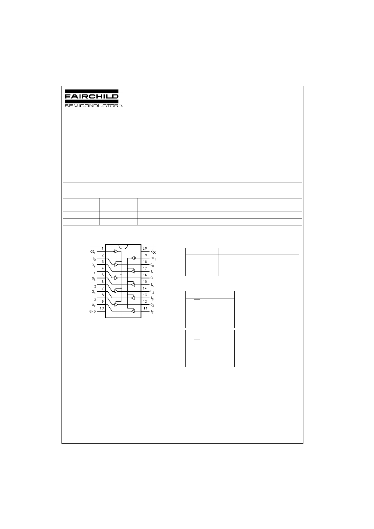
Connection Diagram Pin Descriptions
Truth Tables
H = HIGH Voltage Level
L = LOW Voltage Level
X = Immaterial
Z = High Impedance
Order Number Package Number Package Description
74FR244SC M20B 20-Lead Small Outline Integrated Circuit (SOIC), JEDEC MS-013, 0.300 Wide
74FR244SJ M20D 20-Lead Small Outline Package (SOP), EIAJ TYPE II, 5.3mm Wide
74FR244PC N20A 20-Lead Plastic Dual-In-Line Package (PDIP), JEDEC MS-001, 0.300 Wide
Pin Names Description
OE
1
,–OE
2
Output Enable Input (Active-LOW)
I
0–I7
Inputs
O
0–O7
Outputs
Inputs Outputs
OE
1
I
n
(Pins 12, 14, 16, 18)
LL L
LH H
HX Z
Inputs Outputs
OE
2
I
n
(Pins 3, 5, 7, 9)
LL L
LH H
HX Z
Page 2
www.fairchildsemi.com 2
74FR244
Absolute Maximum Ratings(Note 1) Recommended Operating
Conditions
Note 1: Absolute maximum ratings are values beyond which the device
may be damaged or have its useful life impaired. Functional operation
under these conditi ons is not implied.
Note 2: Either voltage limit or curren t limit is sufficient to protect in put s .
DC Electrical Characteristics
Storage Temperature −65°C to +150°C
Ambient Temperature Under Bias −55°C to +125°C
Junction Temperature Under Bias −55°C to +150°C
V
CC
Pin Potential to Ground Pin −0.5V to +7.0V
Input Voltage (Note 2) −0.5V to +7.0V
Input Current (Note 2) −30 mA to +5.0 mA
Voltage Applied to Output
in HIGH State (with V
CC
= 0V)
Standard Output −0.5V to V
CC
3-STATE Output −0.5V to +5.5V
Current Applied to Output
in LOW State (Max) twice the rated I
OL
(mA)
ESD Last Passing Voltage (Min) 4000V
Free Air Ambient Temperature 0°C to +70°C
Supply Voltage +4.5V to +5.5V
Symbol Parameter Min Typ Max Units
V
CC
Conditions
V
IH
Input HIGH Voltage 2.0 V Recognized HIGH Signal
V
IL
Input LOW Voltage 0.8 V Recognized LOW Signal
V
CD
Input Clamp Diode Voltage −1.2 V Min IIN = −18 mA
V
OH
Output HIGH Voltage 2.4 V Min IOH = −3 mA
2.0 V Min IOH = −15 mA
V
OL
Output LOW Voltage 0.55 V Min IOL = 64 mA
I
IH
Input HIGH Current 5 µAMaxVIN = 2.7V
I
BVI
Input HIGH Current Breakdown Test 7 µAMaxVIN = 7.0V
I
IL
Input LOW Current −150 µAMaxVIN = 0.5V
V
ID
Input Leakage Test 4.75 V 0.0 IID = 1.9 µA,
All Other Pins Grounded
I
OD
Output Circuit Leakage Current 3.75 µA0.0V
IOD
= 150 mV,
All Other Pins Grounded
I
OZH
Output Leakage Current 20 µAMaxV
OUT
= 2.7V
I
OZL
Output Leakage Current −20 µAMaxV
OUT
= 0.5V
I
OS
Output Short-Circuit Current −100 −225 mA Max V
OUT
= 0.0V
I
CEX
Output HIGH Leakage Current 50 µAMaxV
OUT
= V
CC
I
ZZ
Bus Drainage Test 100 µA0.0V
OUT
= 5.25V
I
CCH
Power Supply Current 30 50 mA Max All Outputs HIGH
I
CCL
Power Supply Current 55 75 mA Max All Outputs LOW
I
CCZ
Power Supply Current 35 50 mA Max Outputs 3-STATED
C
IN
Input Capacitance 8.0 pF 5.0
Page 3

3 www.fairchildsemi.com
74FR244
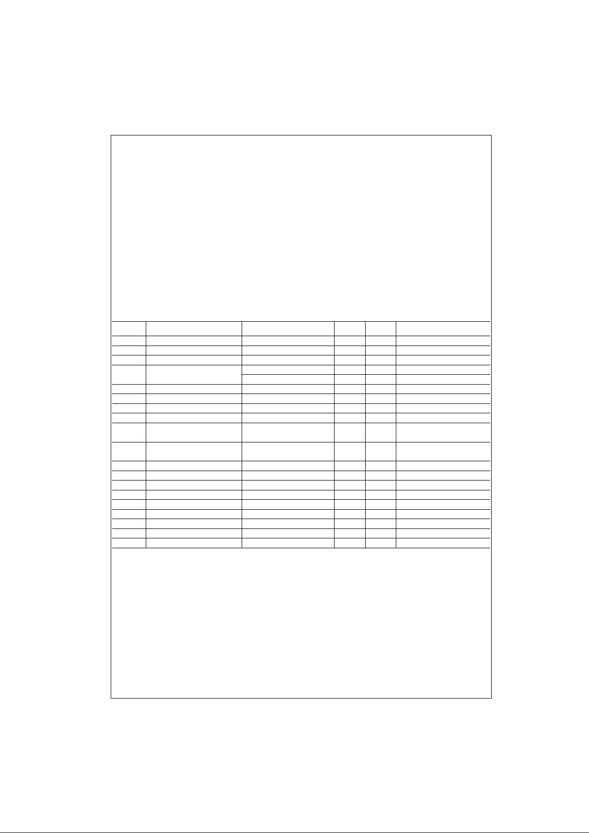
AC Electrical Characteristics
Extended AC Characteristics
Note 3: This specifica ti on is guaranteed but no t tes t ed. The limits apply to pr opagation delays for all pa t hs described switching in phase,
i.e., all LOW-to-HIGH, H IG H -t o-LOW, 3-STATE-to-HIGH, etc.
Note 4: These specific ations guaran teed but no t tested. The limits repres ent propaga tion delays with 250 pF load capacito rs in place of th e 50 pF load
capacitors in the standard AC load. This spe c if ic at ion pertains to single output switching only.
Note 5: Skew is def ined as the abs olute value of the difference betwee n the actual pro pagation delays fo r any two outputs of the same dev ic e. T he specifi-
cation applies to any outputs switching HIGH-to-LOW, (t
OSHL
), LOW-to-HIGH, (t
OSLH
), or HIGH-to-LOW and/or LOW-to-HIGH, (t
OST
). Specification guar an-
teed with all outputs sw it c hing in phase.
Symbol Parameter
TA = +25°CT
A
= 0°C to +70°C
Units
VCC = +5.0V VCC = +5.0V
CL = 50 pF CL = 50 pF
Min Typ Max Min Max
t
PLH
Propagation Delay 1.0 2.6 3.9 1.0 3.9
ns
t
PHL
1.01.83.91.03.9
t
PZH
Output Enable Time 2.5 4.8 6.6 2.5 6.6
ns
t
PZL
2.53.96.62.56.6
t
PHZ
Output Disable Time 1.6 3.7 6.4 1.6 6.4
ns
t
PLZ
1.63.66.41.66.4
Symbol Parameter
TA = 0°C to +70°CTA = 0°C to +70°C
Units
VCC = +5.0V VCC = +5.0V
CL = 50 pF CL = 250 pF
Eight Outputs Switching (Note 4)
(Note 3)
Min Max Min Max
t
PLH
Propagation Delay 1.0 5.0 2.3 7.3
ns
t
PHL
1.0 5.0 2.3 7.3
t
PZH
Output Enable Time 2.5 7.7
ns
t
PZL
2.5 7.7
t
PHZ
Output Disable Time 1.6 6.5
ns
t
PLZ
1.6 6.5
t
OSHL
Pin-to-Pin Skew
1.6 ns
for HL Transitions (Note 5)
t
OSLH
Pin-to-Pin Skew
1.0 ns
for LH Transitions (Note 5)
t
OST
Pin-to-Pin Skew
3.5 ns
for HL/LH Transitions (Note 5)
Page 4

www.fairchildsemi.com 4
74FR244
Physical Dimensions inches (millimeters) unless otherwise noted
20-Lead Small Outline Integrated Circuit (SOIC), JEDEC MS-013, 0.300 Wide
Package Number M20B
20-Lead Small Outline Package (SOP), EIAJ TYPE II, 5.3mm Wide
Package Number M20D
Page 5

5 www.fairchildsemi.com
74FR244 Octal Buffer/Line Driver with 3-STATE Outputs
Physical Dimensions inches (millimeters) unless otherwise noted (Continued)
20-Lead Plastic Dual-In-Line Package (PDIP), JEDEC MS-001, 0.300 Wide
Package Number N20A
Fairchild does not assume any responsibility for use of any circu itry described, no circuit patent license s are implied and
Fairchild reserves the right at any time without notice to change said circuitry and specifications.
LIFE SUPPORT POLICY
FAIRCHILD’S PRODUCTS ARE NOT AUTHORIZED FOR USE AS CRITICAL COMPONENTS IN LIFE SUPPORT
DEVICES OR SYSTEMS WITHOUT THE EXPRESS WRITTEN APPROVAL OF THE PRESIDENT OF FAIRCHILD
SEMICONDUCTOR CORPORATION. As used herein:
1. Life support devices or systems are dev ic es or syste ms
which, (a) are intended for surgical implant into the
body, or (b) support or sustain life, and (c) whose failure
to perform when properly used in accordance with
instructions for use provided i n the labe li ng, can be re asonably expected to result in a significant injury to the
user.
2. A critical componen t in any com ponent o f a l ife supp ort
device or system whose failu re to perform can b e reasonably expected to c ause th e fa i lure of the li fe s upp or t
device or system, or to affect its safety or effectiveness.
www.fairchildsemi.com
 Loading...