

Page 1
© 1999 Fairchild Semiconductor Corporation DS010616 www.fairchildsemi.com
October 1989
Revised August 1999
74FR16541 16-Bit Buffer/Line Driver with 3-STATE Outputs
74FR16541
16-Bit Buffer/Line Driver with 3-STATE Outputs
General Description
The 74FR16541 contains sixteen non-inverting buffers with
3-STATE outputs designed to be emplo yed as a memory
and address driver, clock driver, or bus-oriented tra nsmitter/receiver. The device is byte co ntrolled. Each byte has
separate 3-STATE control inputs which can be shorted
together for full 16-bit operation.
Features
■ Non-inverting buffers
■ 3-STATE outputs drive bus lines
■ Output sink capability of 64 mA, source capability of
15 mA
■ Separate 3-STATE control pins for each byte
■ Guaranteed multiple output switching, 250 pF delays
and pin-to-pin skew
■ 16-bit version of the 74F541, 74F244 or 74FR244
Ordering Code:
Devices also availab le in Tape and Reel. Specify by appending th e s uffix let t er “X” to the ordering code.
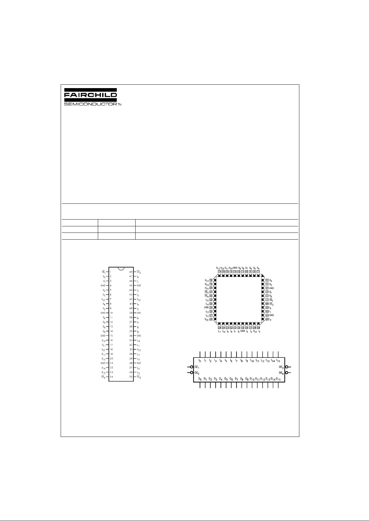
Connection Diagrams
Pin Assignment for SSOP Pin Assignment for PLCC
Logic Symbol
Order Number Package Number Package Description
74FR16541QC V44A 44-Lead Plastic Lead Chip Carrier (PLCC), JEDEC MO-047, 0.650 Square
74FR16541SSC MS48A 48-Lead Small Shrink Outline Package (SSOP), JEDEC MO-118, 0.300 Wide
Page 2
www.fairchildsemi.com 2
74FR16541
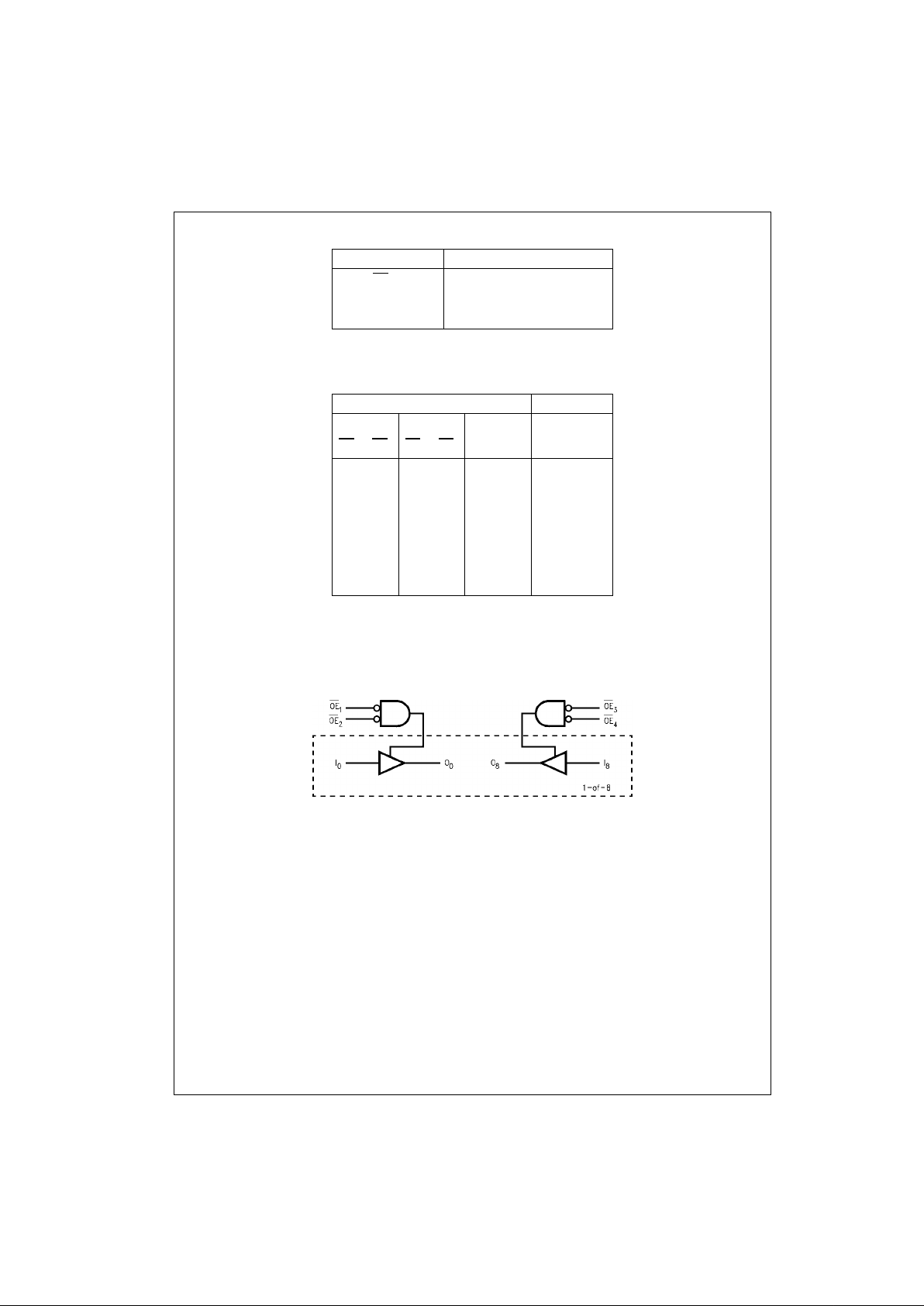
Pin Descriptions
Truth Table
H = HIGH Voltage Level
L = LOW Voltage Level
X = Immaterial
Z = High Impedance
Logic Diagram
Pin Names Description
OE
n
Output Enable Inputs
I
0–I15
Inputs
O
0–O15
3-STATE Outputs
Inputs Outputs
Byte1 [0:7] Byte2 [8:15] I
0–I7I8–I15O0–O7O8–O15
OE1OE2OE3OE
4
LLLLHHH H
HXL LXL Z L
XHL LXH Z H
LLHXLXL Z
LLXHHXH Z
HHHHXX Z Z
LLLLLL L L
Page 3

3 www.fairchildsemi.com
74FR16541
Absolute Maximum Ratings(Note 1) Recommended Operating
Conditions
Note 1: Absolute maximum ratings are values beyon d which the device
may be damaged or have its useful life impaired . Functional operation
under these condit ions is not implied.
Note 2: Either voltage limit or curren t limit is sufficient to protect in puts.
DC Electrical Characteristics
Storage Temperature −65°C to +150°C
Ambient Temperature under Bias −55°C to +125°C
Junction Temperature under Bias −55°C to +150°C
V
CC
Pin Potential to Ground Pin −0.5V to +7.0V
Input Voltage (Note 2) −0.5V to +7.0V
Input Current (Note 2) −30 mA to +5.0 mA
Voltage Applied to Output
in HIGH State (with V
CC
= 0V)
Standard Output −0.5V to V
CC
3-STATE Output −0.5V to +5.5V
Current Applied to Output
in LOW State (Max) Twice the Rated I
OL
(mA)
ESD Last Passing Voltage (Min) 4000V
Free Air Ambi ent Temperat ure 0°C to +70°C
Supply Voltage +4.5V to +5.5V
Symbol Parameter Min Typ Max Units
V
CC
Conditions
V
IH
Input HIGH Voltage 2.0 V Recognized as a HIGH Signal
V
IL
Input LOW Voltage 0.8 V Recognized as a LOW Signal
V
CD
Input Clamp Diode Voltage −1.2 V Min IIN = −18 mA
V
OH
Output HIGH 2.4
VMin
IOH = −3 mA
Voltage 2.0 IOH = −15 mA
V
OL
Output LOW Voltage 0.55 V Min IOL = 64 mA
I
IH
Input HIGH Current 5.0 µAMaxVIN = 2.7V
I
BVI
Input HIGH Current
7.0 µAMax
VIN = 7.0V
Breakdown Test
(OEn)
I
IL
Input LOW Current −120 µAMaxVIN = 0.5V
I
OS
Output Short-Circuit
−100 −225 mA Max V
OUT
= 0V
Current
I
OZH
Output Leakage Current 0 20 µAMaxV
OUT
= 2.7V
I
OZL
Output Leakage Current 0 −20 µAMaxV
OUT
= 0.5V
I
CEX
Output HIGH Leakage Current 50 µAMaxV
OUT
= V
CC
V
ID
Input Leakage Test 4.75 V 0.0 IID = 1.9 µA
All Other Pins Grounded
I
OD
Output Circuit Leakage Current 3.75 µA0.0V
IOD
= 150 mV
All Other Pins Grounded
I
ZZ
Bus Drainage Test 100 µA0.0V
OUT
= 5.25V
I
CCH
Power Supply Current 35 50 mA Max VO = HIGH
I
CCL
Power Supply Current 92 110 mA Max VO = LOW
I
CCZ
Power Supply Current 36 50 mA Max VO = HIGH Z
C
IN
Input Capacitance 8 pF 5.0
Page 4

www.fairchildsemi.com 4
74FR16541
AC Electrical Characteristics
Extended AC Characteristics
Note 3: Skew is defined as the absolute value of t he difference betw een the actual p ropagation delays f or any two outp ut s of the same device. T he specifi-
cation applies to an y outputs swit ching HIGH- to-LOW, (t
osHL
), LOW-to-HIGH, ( t
osLH
), or HIGH-to-LOW and/or LOW-to-HIGH, (t
ost
). Specifications gu aranteed with all outputs switching in phase.
Note 4: This specific ation is guaranteed b ut not t es t ed. The limits apply to propagation delays for all paths described swit ch ing in phase,
i.e., all LOW-to-HIGH , H IG H -t o-LOW, 3-STATE-to-HIGH, etc.
Note 5: These specific ations guarant eed but no t tested. The limits repres ent propaga tion delays wi th 250 pF l oad capacitors in place of the 50 pF load
capacitors in the standard AC load. This s pecification pertains to s ingle output switching only.
Symbol Parameter
TA = +25°CT
A
= 0°C to +70°C
Units
VCC = +5.0V VCC = +5.0V
CL = 50 pF CL = 50 pF
Min Typ Max Min Max
t
PLH
Propagation Delay 1.5 2.8 4.3 1.5 4.3
ns
t
PHL
In to O
n
1.5 2.4 4.3 1.5 4.3
t
PZH
Output Enable Time 3.6 5.8 11.6 3.6 11.6
ns
t
PZL
3.6 6.6 11.6 3.6 11.6
t
PHZ
Output Disable Time 1.8 4.0 6.6 1.8 6.6
ns
t
PLZ
1.8 4.1 6.6 1.8 6.6
Symbol Parameter
TA = 0°C to +70°CTA = 0°C to +70°C
Units
VCC = +5.0V VCC = +5.0V
CL = 50 pF CL = 250 pF
16 Outputs Switching
(Note 4) (Note 5)
Min Max Min Max
t
PLH
Propagation Delay 1.5 5.7 3.0 9.0
ns
t
PHL
An to Bn or Bn to A
n
1.55.73.09.0
t
PZH
Output Enable Time 3.6 12.5
ns
t
PZL
3.6 12.5
t
PHZ
Output Disable Time 1.8 6.6
ns
t
PLZ
1.8 6.6
t
osHL
Pin-to-Pin Skew
1.5 ns
(Note 3) for HL Transitions
t
osLH
Pin-to-Pin Skew
1.3 ns
(Note 3) for LH Transitions
t
ost
Pin-to-Pin Skew
2.0 ns
(Note 3) for HL/LH Transitions
Page 5

5 www.fairchildsemi.com
74FR16541
Physical Dimensions inches (millimeters) unless otherwise noted
44-Lead Plastic Lead Chip Carrier (PLCC), JEDEC MO-047, 0.650 Square
Package Number V44A
Page 6

www.fairchildsemi.com 6
74FR16541 16-Bit Buffer/Line Driver with 3-STATE Outputs
Physical Dimensions inches (millimeters) unless otherwise noted (Continued)
48-Lead Small Shrink Outline Package (SSOP), JEDEC MO-118, 0.300 Wide
Package Number MS48A
Fairchild does not assume any responsibility for use of any circuitry described, no circuit pate nt licenses are implied and
Fairchild reserves the right at any time without notice to change said circuitry and specifications.
LIFE SUPPORT POLICY
FAIRCHILD’S PRODUCTS ARE NOT AUTHORIZED FOR USE AS CRITICAL COMPONENTS IN LIFE SUPPORT
DEVICES OR SYSTEMS WITHOUT THE EXPRESS WRITTEN APPROVAL OF THE PRESIDENT OF FAIRCHILD
SEMICONDUCTOR CORPORATION. As used herein:
1. Life support devices or systems are devices or systems
which, (a) are intended for surgical implant into the
body, or (b) support or sustain life, and (c) whose failure
to perform when properly used in accordance with
instructions for use provided in the labeling, can be reasonably expected to result in a significant inju ry to the
user.
2. A critical component in any componen t of a life su pport
device or system whose failu re to perform can be reasonably expected to ca use the fa i lure of the life su pp ort
device or system, or to affect its safety or effectiveness.
www.fairchildsemi.com
 Loading...