

Page 1
© 1999 Fairchild Semiconductor Corporation DS010977 www.fairchildsemi.com
March 1992
Revised August 1999
74FR74 • 74FR1074 Dual D-Type Flip-Flop
74FR74 • 74FR1074
Dual D-Type Flip-Flop
General Description
The 74FR74 and 74 FR107 4 are dua l D-ty pe flip-f lops with
true and complement (Q/Q
) outputs. On the 74F R74, data
at the D inputs is transferred t o the outputs on the rising
edge of the clock inpu t (CP
n
). The 74FR1074 is the neg a-
tive edge triggered version of this device. Both parts feature asynchronous clear (C
Dn
) and set (SDn) inputs which
are low level enabled.
Features
■ 74FR74 is pin-for-pin compatible with the 74F74
■ True 150 MHz f
MAX
capability on 74FR74
■ Outputs sink 24 mA and source 24 mA
■ Guarante ed pin-to-pin skew specifications
Ordering Code:
Devices also availab le in Tape and Reel. Specify by appending th e s uffix let t er “X” to the ordering code.
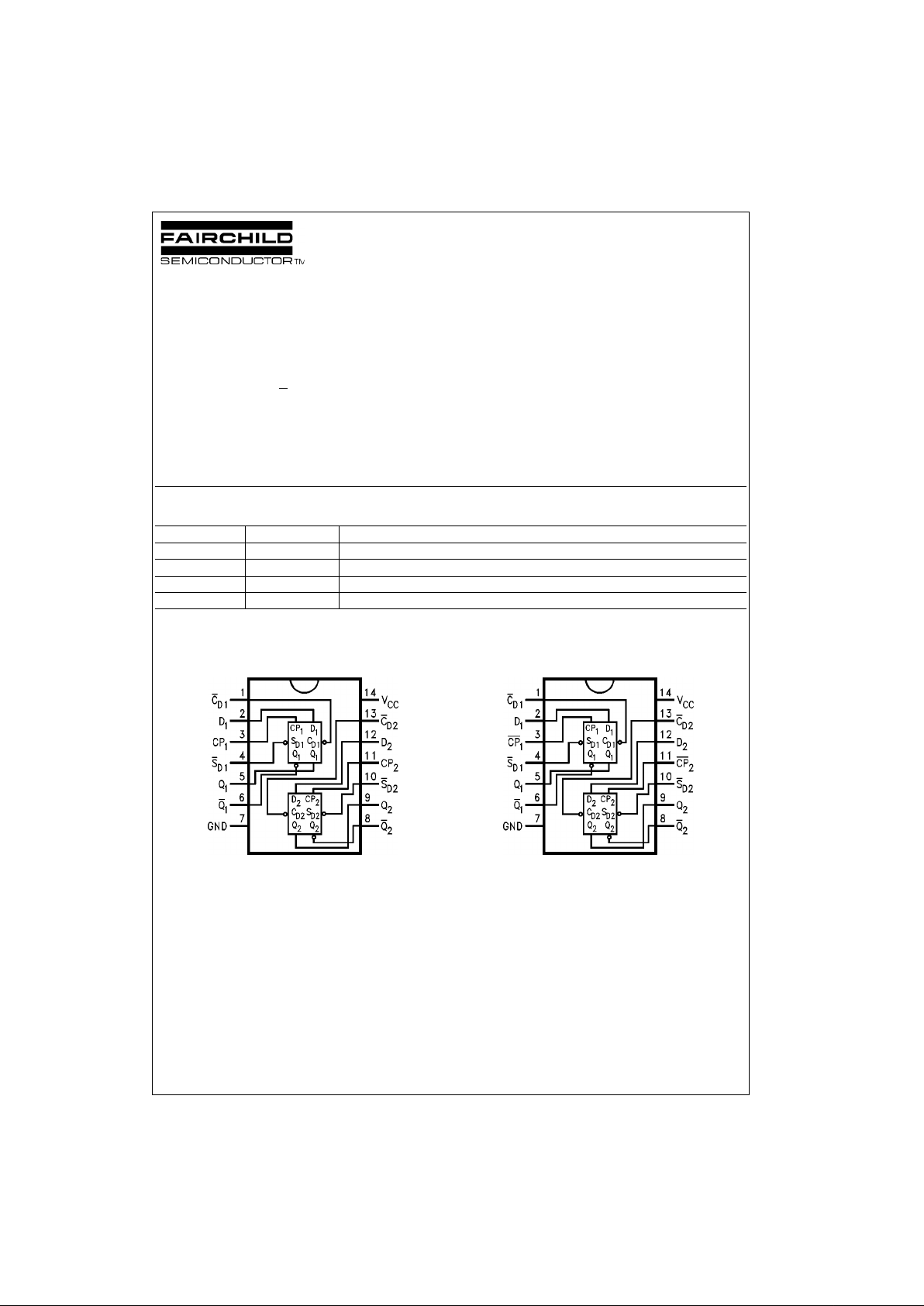
Connection Diagrams
74FR74 74FR1074
Order Number Package Number Package Description
74FR74SC M14A 14-Lead Small Outline Integrated Circuit (SOIC), JEDEC MS-120, 0.150 Narrow
74FR74PC N14A 14-Lead Plastic Dual-In-Line Package (PDIP), JEDEC MS-001, 0.300 Wide
74FR1074SC M14A 14-Lead Small Outline Integrated Circuit (SOIC), JEDEC MS-120, 0.150 Narrow
74FR1074PC N14A 14-Lead Plastic Dual-In-Line Package (PDIP), JEDEC MS-001, 0.300 Wide
Page 2
www.fairchildsemi.com 2
74FR74 • 74FR1074
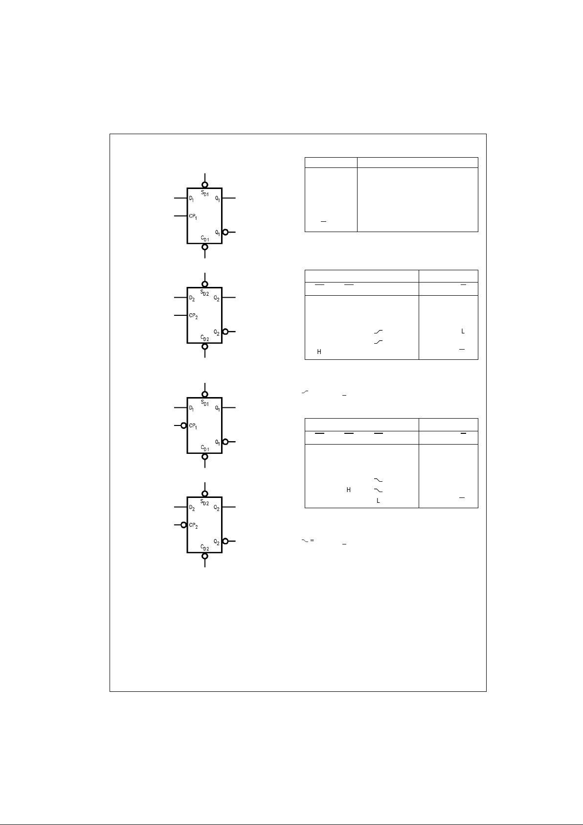
Logic Symbols
74FR74
74FR1074
Pin Descriptions
Tr uth Tables
74FR74
H = HIGH Voltage Level
L = LOW Voltage Level
Z = High Impedance
X = Immaterial
= Rising Edge
Q
0
= Previous Q(Q) before LOW-to-HIGH Clock Transition
74FR1074
H = HIGH Voltage Level
L = LOW Voltage Level
Z = High Impedance
X = Immaterial
= Falling Edge
Q
0
= Previous Q(Q) before HIGH-to-LOW Clock Transition
Pin Names Description
D
n
Data Inputs
CP
n
Clock Inputs
S
Dn
Asynchronous Set Inputs
C
Dn
Asynchronous Clear Inputs
Q
n
True Output
Q
n
Complementary Output
Inputs Outputs
SD
CD CP D Q Q
LHXXHL
HLXXLH
LLXXHH
HH
HH L
HH
LLH
HHLXQ
0
Q
0
Inputs Outputs
SD
CD CP DQ Q
LHXXHL
HLXXLH
LLXXHH
HH
HH L
HH
LLH
HHLXQ
0
Q
0
Page 3
3 www.fairchildsemi.com
74FR74 • 74FR1074
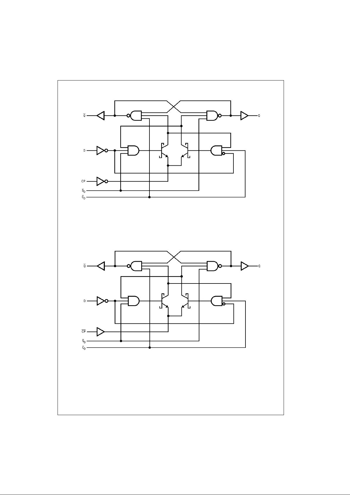
Logic Diagrams
74FR74
74FR1074
Please note that thes e diagrams are provide d only for the understan ding of logic operations a nd should not be used to es t im ate propagation delays.
Page 4

www.fairchildsemi.com 4
74FR74 • 74FR1074
Absolute Maximum Ratings(Note 1) Recommended Operating
Conditions
Note 1: Absolute maximum ratings are values beyond which the device
may be damaged or have its useful life impaired. Functional operation
under these conditi ons is not implied.
Note 2: Either voltage limit or curren t limit is sufficient to protect in put s .
DC Electrical Characteristics
Storage Temperature −65°C to +150°C
Ambient Temperature under Bias −55°C to +125°C
Junction Temperature under Bias −55°C to +150°C
V
CC
Pin Potential to Ground Pin −0.5V to +7.0V
Input Voltage (Note 2) −0.5V to +7.0V
Input Current (Note 2) −30 mA to +5.0 mA
Voltage Applied to Output
in HIGH State (with V
CC
= 0V)
Standard Output −0.5V to V
CC
Current Applied to Output
in LOW State (Max) twice the rated I
OL
(mA)
ESD Last Passing Voltage (Min) 2000V
Free Air Ambient Temperature 0°C to +70°C
Supply Voltage +4.5V to +5.5V
Symbol Parameter Min Typ Max Units
V
CC
Conditions
V
IH
Input HIGH Voltage 2.0 V Recognized HIGH Signal
V
IL
Input LOW Voltage 0.8 V Recognized LOW Signal
V
CD
Input Clamp Diode Voltage −1.2 V Min IIN = −18 mA
V
OH
Output HIGH 2.5 V Min IOH = −1 mA
Voltage 2.4 V Min IOH = −3 mA
2.0 V Min IOH = −24 mA
V
OL
Output LOW Voltage 0.5 V Min IOL = 24 mA
I
IH
Input HIGH Current 5 µAMaxVIN = 2.7V
I
BVI
Input HIGH Current
7 µAMaxVIN = 7.0V
Breakdown Test
I
IL
Input LOW Current −150 µAMaxVIN = 0.5V (Dn, CPn)
−1.8 mA Max VIN = 0.5V (CDn, SDn)
V
ID
Input Leakage Test 4.75 V 0.0 IID = 1.9 µA,
All Other Pins Grounded
I
OD
Output Circuit 3.75 V 0.0 V
IOD
= 150 mV,
Leakage Test All Other Pins Grounded
I
OS
Output Short-Circuit Current −100 −275 mA Max V
OUT
= 0.0V
I
CEX
Output HIGH 50 µAMaxV
OUT
= V
CC
Leakage Current
I
CC
Power Supply Current 24 mA Max
Page 5

5 www.fairchildsemi.com
74FR74 • 74FR1074
AC Electrical Characteristics 74FR74
Note 3: Pin-to-Pin S kew is d efine d as the a bso lute va lue of the differ ence bet wee n the actua l pr opaga tion de lay for any o utpu ts within the same packaged
device. The specifications apply to any outputs switching in the same direction either HIGH-to-LOW (t
OSHL
) or LOW-to-HIGH (t
OSLH
) or in opposite directions
both HL and LH (t
OST
). t
OST
is guaranteed by des ign.
AC Operating Requirements 74FR74
Note 4: This specifica ti on is guaranteed by design.
Symbol Parameter
TA = +25°CT
A
= 0°C to +70°C
Units
VCC = +5.0V VCC = +5.0V
CL = 50 pF CL = 50 pF
Min Typ Max Min Max
f
MAX
Maximum Clock Frequency 150 190 150 MHz
t
PLH
Propagation Delay 2.5 3.5 5.0 2.5 5.0
ns
t
PHL
CPn to Qn or Q
n
2.54.56.02.56.0
t
PLH
Propagation Delay 1.5 3.5 5.5 1.5 5.5
ns
t
PHL
CDn or SDn to Qn or Q
n
2.05.57.02.07.0
t
OSHL
Pin to Pin Skew
1.0 ns
(Note 3) for HL Transitions
t
OSLH
Pin to Pin Skew
1.0 ns
(Note 3) for LH Transitions
t
OST
Pin to Pin Skew
3.0 ns
(Note 3) for HL/LH Transitions
t
Q/Q
True/Complement
1.8 ns
(Note 3) Output Skew
t
PS
Pin (Signal)
1.8 ns
(Note 3) Transition Variation
Symbol Parameter
TA = +25°CT
A
= 0°C to +70°C
Units
VCC = +5.0V VCC = +5.0V
CL = 50 pF CL = 50 pF
MinMaxMinMax
tS(H) Setup Time, HIGH or LOW 2.5 2.5
ns
tS(L) Dn to CP
n
2.5 2.5
tH(H) Hold Time, HIGH or LOW 0 0
ns
tH(L) Dn to CP
n
00
tW(H) CPn Pulse Width 3.3 3.3
ns
tW(L) HIGH or LOW 3.3 3.3
(Note 4)
tW(L)
SDn or CDn Pulse Width
4.0 4.0 ns
t
REC
Recovery Time 2.0 2.0 ns
SDn or CDn to CP
n
Page 6

www.fairchildsemi.com 6
74FR74 • 74FR1074
AC Electrical Characteristics 74FR1074
Note 5: Pin-to-Pin Skew is def ined a s th e abs olut e va lue of the differenc e be twe en t he ac tua l propa ga tion d elay for a ny o utpu ts wi thin the same packaged
device. The specifications apply to any outputs switching in the same direction either HIGH-to-LOW (t
OSHL
) or LOW-to-HIGH (t
OSLH
) or in opposite directions
both HL and LH (t
OST
). t
OST
is guaranteed by desi gn.
AC Operating Requirements 74FR1074
Note 6: This specific ation is guaranteed b y des ign.
Symbol Parameter
TA = +25°CT
A
= 0°C to +70°C
Units
VCC = +5.0V VCC = +5.0V
CL = 50 pF CL = 50 pF
Min Typ Max Min Max
f
MAX
Maximum Clock Frequency 120 160 120 MHz
t
PLH
Propagation Delay 2.5 4.0 5.5 2.5 5.5
ns
t
PHL
CPn to Qn or Q
n
3.0 5.0 6.5 3.0 6.5
t
PLH
Propagation Delay 1.5 3.5 5.5 1.5 5.5
ns
t
PHL
CDn or SDn to Qn or Q
n
2.0 5.5 7.0 2.0 7.0
t
OSHL
Pin to Pin Skew
1.5 ns
(Note 5) for HL Transitions
t
OSLH
Pin to Pin Skew
1.5 ns
(Note 5) for LH Transitions
t
OST
Pin to Pin Skew
3.5 ns
(Note 5) for HL/LH Transitions
t
Q/Q
True/Complement
2.0 ns
(Note 5) Output Skew
t
PS
Pin (Signal)
2.0 ns
(Note 5) Transition Variation
TA = +25°CT
A
= 0°C = +70°C
Symbol Parameter VCC = +5.0V VCC = +5.0V Units
CL = 50 pF CL = 50 pF
Min Max Min Max
tS(H) Setup Time, HIGH or LOW 2.0 2.0
ns
tS(L) Dn to CP
n
2.0 2.0
tH(H) Hold Time, HIGH or LOW 0 0
ns
tH(L) Dn to CP
n
00
tW(H)
CPn Pulse Width
3.3 3.3
ns
tW(L) HIGH or LOW 3.3 3.3
(Note 6)
tW(L)
SDn or CDn Pulse Width
4.0 4.0 ns
t
REC
Recovery Time
2.0 2.0 ns
SDn or CDn to CP
n
Page 7

7 www.fairchildsemi.com
74FR74 • 74FR1074
Physical Dimensions inches (millimeters) unless otherwise noted
14-Lead Small Outline Integrated Circuit (SOIC), JEDEC MS-120, 0.150 Narrow
Package Number M14A
Page 8

www.fairchildsemi.com 8
74FR74 • 74FR1074 Dual D-Type Flip-Flop
Physical Dimensions inches (millimeters) unless otherwise noted (Continued)
14-Lead Plastic Dual-In-Line Package (PDIP), JEDEC MS-001, 0.300 Wide
Package Number N14A
Fairchild does not assume any responsibility for use of any circuitry described, no circuit pate nt licenses are implied and
Fairchild reserves the right at any time without notice to change said circuitry and specifications.
LIFE SUPPORT POLICY
FAIRCHILD’S PRODUCTS ARE NOT AUTHORIZED FOR USE AS CRITICAL COMPONENTS IN LIFE SUPPORT
DEVICES OR SYSTEMS WITHOUT THE EXPRESS WRITTEN APPROVAL OF THE PRESIDENT OF FAIRCHILD
SEMICONDUCTOR CORPORATION. As used herein:
1. Life support devices or systems are devices or syste ms
which, (a) are intended for surgical implant into the
body, or (b) support or sustain life, and (c) whose failure
to perform when properly used in accordance with
instructions for use provided in the labeling, can be reasonably expected to result in a significant inju ry to the
user.
2. A critical component i n any compon ent of a lif e support
device or system whose failu re to perform can be reasonably expected to ca use the fa i lure of the life su pp ort
device or system, or to affect its safety or effectiveness.
www.fairchildsemi.com
 Loading...