

Datasheet 74F899SCX, 74F899SC, 74F899QCX, 74F899QC, 74F899PC Datasheet (Fairchild Semiconductor)
Page 1
© 1999 Fairchild Semiconductor Corporation DS010195 www.fairchildsemi.com
February 1989
Revised August 1999
74F899 9-Bit Latchable Transceiver
74F899
9-Bit Latchable Transceiver
with Parity Generator/Checker
General Description
The 74F899 is a 9-bi t to 9-bit pa rity transcei ver with t ransparent latches. The device can operate as a feed-thr ough
transceiver or it can generat e/check parity from the 8-bit
data busses in either d i rect ion. It ha s a guaranteed curre nt
sinking capability of 24 mA at the A-bus and 64 mA a t the
B-bus.
The 74F899 features independent latch enables for the
A-to-B direction an d the B-to-A direction, a sel ect pin for
ODD/EVEN
parity, and separate error signal output pins for
checking parity.
Features
■ Latchable transceiver with output sink of 24 mA at the
A-bus and 64 mA at the B-bus
■ Option to select generate parity and check or
“feed-through” data/parity in directions A-to-B or B-to-A
■ Independent latch enables for A-to-B and B-to-A
directions
■ Select pin for ODD/EVEN
parity
■ ERRA
and ERRB output pins for parity checking
■ Ability to simultaneously generate and check parity
■ May be used in systems applications in place of the
74F543 and 74F280
■ May be used in system applications in place of the
74F657 and 74F3 73 (no need to chang e T/R
to check
parity)
Ordering Code:
Devices also availab le in Tape and Reel. Specify by appending th e s uffix let t er “X” to the ordering code.
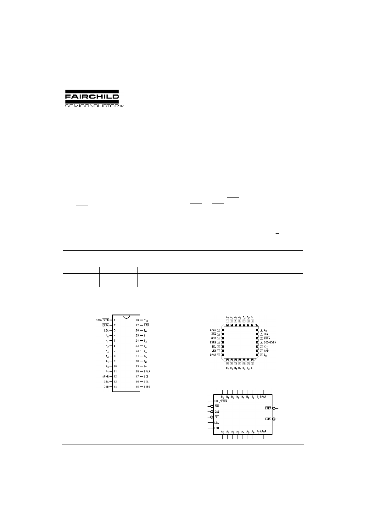
Connection Diagrams
Pin Assignment for SOIC Pin Assignment for PCC
Logic Symbol
Order Number Package Number Package Description
74F899SC M28B 28-Lead Small Outline Integrated Circuit (SOIC), JEDEC MS-013, 0.300 Wide
74F899QC V28A 28-Lead Plastic Lead Chip Carrier (PLCC), JEDEC MO-047, 0.450 Square
Page 2
www.fairchildsemi.com 2
74F899
Input Loading/Fan-Out
Pin Descriptions
Functional Description
The 74F899 has t hree principal modes of ope ration which
are outlined below. These modes a pply to both the A -to-B
and B-to-A directions.
• Bus A (B) communicates to Bus B (A), parity is gener ated and passed on to the B (A) Bus as BPAR (APAR). If
LEB (LEA) is HIGH and the Mode Select (SEL
) is LOW,
the parity generated from B[0:7] (A[0:7]) can be checked
and monitored by ERRB
(ERRA).
• Bus A (B) communicates to Bus B (A) in a feed-th rough
mode if SEL
is HIGH. Parity is still generated and
checked as ERRA
and ERRB in the feed-through mode
(can be used as an interru pt to signal a data/parity bit
error to the CPU).
• Independent Latch Ena bles (LEA and LEB) allow oth er
permutations of generating/checking (see Function
Table).
HIGH/LOW
Pin Names Description U.L.
Input I
IH/IIL
HIGH/LOW
Output I
OH/IOL
A0–A
7
Data Inputs/ 1.0/1.0 20 µA/−0.6 mA
Data Outputs 150/40 −3 mA/24 mA
B
0–B7
Data Inputs/ 1.0/1.0 20 µA/−0.6 mA
Data Outputs 600/106.6 −12 mA/64 mA
APAR A Bus Parity 1.0/1.0 20 µA/−0.6 mA
Input/Output 150/40 −3 mA/24 mA
BPAR B Bus Parity 1.0/1.0 20 µA/−0.6 mA
Input/Output 600/106.6 −12 mA/64 mA
ODD/EVEN
Parity Select Input 1.0/1.0 20 µA/−0.6 mA
GBA
, GAB
Output Enable Inputs 1.0/1.0 20 µA/−0.6 mA
SEL
Mode Select Input 1.0/1.0 20 µA/−0.6 mA
LEA, LEB Latch Enable Inputs 1.0/1.0 20 µA/−0.6 mA
ERRA
, ERRB
Error Signal Outputs 50/33.3 −1 mA/20 mA
Pin Names Description
A
0–A7
A Bus Data Inputs/Data Outputs
B
0–B7
B Bus Data Inputs/Data Outputs
APAR, BPAR A and B Bus Parity Inputs
ODD/EVEN
ODD/EVEN Parity Select, Active LOW for EVEN Parity
GBA
, GAB Output Enables for A or B Bus, Active LOW
SEL
Select Pin for Feed-Through or Generate Mode, LOW for Generate Mode
LEA, LEB Latch Enables for A and B Latches, HIGH for Transparent Mode
ERRA
, ERRB Error Signals for Checking Generated Parity with Parity In, LOW if Error Occurs
Page 3
3 www.fairchildsemi.com
74F899
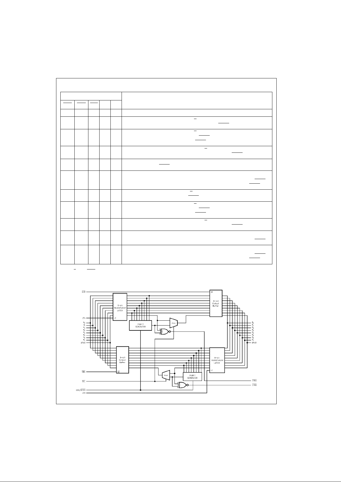
Function Table
H = HIGH Voltage Level L = LOW Voltage Level X = Immaterial
Note 1: O/E
= ODD/EVEN
Functional Block Diagram
Inputs
Operation
GAB
GBA SEL LEA LEB
H H X X X Busses A and B are 3-STATE.
HLLLH
Generates parity from B[0:7] based on O/E
(Note 1). Generated parity → APAR.
Generated parity checked against BPAR and output as ERRB
.
H L L H H Generates parity from B[0:7] based on O/E
. Generated parity → APAR. Generated
parity checked against BPAR and output as ERRB
. Generated parity also fed back
through the A latch for generate/check as ERRA
.
HLLXL
Generates parity from B latch data based on O/E
. Generated parity → APAR.
Generated parity checked against latched BPAR and output as ERRB
.
HLHXHBPAR/B[0:7] → APAR/A0:7] Feed-through mode. Generated parity checked against
BPAR and output as ERRB
.
H L H H H BPAR/B[0:7] → APAR/A[0:7]
Feed-through mode. Generated parity checked against BPAR and output as ERRB
.
Generated parity also fed back through the A latch for generate/check as ERRA
.
L H L H L Generates parity for A[0:7] based on O/E
. Generated parity → BPAR. Generated parity
checked against APAR and output as ERRA
.
L H L H H Generates parity from A[0:7] based on O/E
. Generated parity → BPAR. Generated
parity checked against APAR and output as ERRA
. Generated parity also fed back
through the B latch for generate/check as ERRB
.
L H L L X Generates parity from A latch data based on O/E
. Generated parity → BPAR.
Generated parity checked against latched APAR and output as ERRA
.
LHHHLAPAR/A[0:7] → BPAR/B[0:7]
Feed-through mode. Generated parity checked against APAR and output as ERRA
.
L H H H H APAR/A[0:7] → BPAR/B[0:7]
Feed-through mode. Generated parity checked against APAR and output as ERRA
.
Generated parity also fed back through the B latch for generate/check as ERRB
.
Page 4
www.fairchildsemi.com 4
74F899
Absolute Maximum Ratings(Note 2) Recommended Operating
Conditions
Note 2: Absolute maximum ratings are values beyond which the device
may be damaged or have its useful life impaired. Functional operation
under these conditi ons is not implied.
Note 3: Either voltage limit or curren t limit is sufficient to protect in put s .
DC Electrical Characteristics
Storage Temperature −65°C to +150°C
Ambient Temperature under Bias −55°C to +125°C
Junction Temperature under Bias −55°C to +150°C
V
CC
Pin Potential to Ground Pin −0.5V to +7.0V
Input Voltage (Note 3) −0.5V to +7.0V
Input Current (Note 3) −30 mA to +5.0 mA
Voltage Applied to Output
in HIGH State (with V
CC
= 0V)
Standard Output −0.5V to V
CC
3-STATE Output −0.5V to +5.5V
Current Applied to Output
in LOW State (Max) Twice the Rated I
OL
(mA)
ESD Last Passing Voltage (Min) 4000V
Free Air Ambient Temperature 0°C to +70°C
Supply Voltage +4.5V to +5.5V
Symbol Parameter Min Typ Max Units
V
CC
Conditions
V
IH
Input HIGH Voltage 2.0 V Recognized as a
HIGH Signal
V
IL
Input LOW Voltage 0.8 V Recognized as a
LOW Signal
V
CD
Input Clamp Diode Voltage −1.2 V Min IIN = −18 mA
V
OH
Output HIGH 10% V
CC
2.5 IOH = −1 mA
Voltage 10% V
CC
2.4 IOH = −3 mA
10% V
CC
2.0 V IOH = −15 mA (Bn, BPAR)
5% V
CC
2.7 IOH = −1 mA
5% V
CC
2.7 IOH = −3 mA
V
OL
Output LOW 10% V
CC
0.5 IOL = 20 mA
Voltage
(An, APAR, ERRA, ERRB)
5% V
CC
0.55 V IOL = 24 mA
(An, APAR, ERRA, ERRB)
10% V
CC
0.55 IOL = 64 mA (Bn, BPAR)
V
TH
Input Threshold Voltage 1.45 V ±0.1V, Sweep Edge Rate must be > 1V/50 ns
V
OLV
Negative Ground Bounce
1.0 V
Observed on “quiet” output during
Voltage simultaneous switching of remaining outputs
V
OLP
Positive Ground Bounce
1.0 V
Observed on “quiet” output during
Voltage simultaneous switching of remaining outputs
I
IL
Input Low Current −0.6 mA Max VIN = 0.5V
I
IH
Input HIGH
5.0 µAMaxVIN = 2.7V
Current
I
BVI
Input HIGH Current
7.0 µAMax
VIN = 7.0V
Breakdown Test
(ODD/EVEN, GBA, GAB, SEL, LEA, LEB)
I
BVIT
Input HIGH Current
0.5 mA Max
VIN = 5.5V
Breakdown (I/O) (An, Bn, A
PAR
, B
PAR
)
I
CEX
Output HIGH
50 µAMaxV
OUT
= V
CC
Leakage Current
V
ID
Input Leakage
4.75 V 0.0
IID = 1.9 µA
Test All Other Pins Grounded
I
OD
Output Leakage
3.75 µA0.0
V
IOD
= 150 mV
Circuit Current All Other Pins Grounded
I
IL
Input Low Current −0.6 mA Max VIN = 0.5V
I
IH+
Output Leakage Current
70 µAMax
V
I/O
= 2.7V
I
OZH
Current (An, Bn, APAR, BPAR)
Page 5

5 www.fairchildsemi.com
74F899
DC Electrical Characteristics (Continued)
AC Electrical Characteristics
Symbol Parameter Min Typ Max Units
V
CC
Conditions
I
IL+
Output Leakage
−650 µAMax
V
I/O
= 0.5V
I
OZL
Current (An, Bn, APAR, BPAR)
I
OS
Output Short-Circuit Current −60 −150 Max V
OUT
= 0V
mA
(An, APAR, ERRA, ERRB)
−100 −225 Max V
OUT
= 0V (Bn, BPAR)
I
ZZ
Bus Drainage Test 500 µA0.0VV
OUT
= 5.25V
I
CCH
Power Supply Current 132 155 mA Max VO = HIGH
I
CCL
Power Supply Current 178 210 mA Max VO = LOW, GAB = LOW,
GBA = HIGH, VIL = LOW
I
CCZ
Power Supply Current 160 190 mA Max VO = HIGH Z
Symbol Parameter
TA = +25°CT
A
= 0°C to +70°C
Units
Figure
Number
VCC = +5.0V VCC = +5.0V
CL = 50 pF CL = 50 pF
Min Typ Max Min Max
t
PLH
Propagation Delay 4.0 7.5 13.0 4.0 14.0
ns Figure 1
t
PHL
An, APAR to Bn, BPAR 4.0 8.5 13.0 4.0 14.0
t
PLH
Propagation Delay 7.5 12.0 17.0 7.5 18.0
ns Figure 2
t
PHL
An, Bn to BPAR, APAR 7.5 12.5 17.0 7.5 18.0
t
PLH
Propagation Delay 7.5 12.0 17.0 7.5 18.0
ns Figure 3
t
PHL
An, Bn to ERRA, ERRB
7.5 12.5 17.0 7.5 18.0
t
PLH
Propagation Delay 4.5 7.5 11.0 4.5 12.0
ns Figure 4
t
PHL
ODD/EVEN to ERRA, ERRB
4.5 8.0 11.0 4.5 12.0
t
PLH
Propagation Delay 4.5 7.5 11.5 4.5 12.5
ns Figure 5
t
PHL
ODD/EVEN to APAR, BPAR
4.5 8.5 11.5 4.5 12.5
t
PLH
Propagation Delay 5.5 9.0 13.0 5.5 14.0
ns Figure 6
t
PHL
APAR, BPAR to ERRA, ERRB
5.5 9.5 13.0 5.5 14.0
t
PLH
LEA/LEB to 9.5 13.0 17.5 7.5 18.0
ns Figure 7
t
PHL
ERRA /ERRB
9.7 17.5 7.5 18.0
t
PLH
Propagation Delay 3.0 6.0 10.0 3.0 11.0
ns Figure 10
t
PHL
SEL to APAR, BPAR
3.0 7.0 10.0 3.0 11.0
t
PLH
Propagation Delay 3.5 7.0 10.0 3.5 11.0
ns Figure 11
t
PHL
LEB to An, APAR 3.5 8.0 10.0 3.5 11.0
t
PLH
t
PHL
Propagation Delay 3.5 6.5 10.0 3.5 11.0
ns Figure 11
LEA to Bn, BPAR 3.5 7.5 10.0 3.5 11.0
t
PZH
Output Enable Time 1.0 4.5 10.0 1.0 11.0
ns
Figure 8,
Figure 9
t
PZL
GBA or GAB to An,
1.0 6.5 10.0 1.0 11.0
APAR or Bn, BPAR
t
PHZ
Output Disable Time 1.0 4.0 7.0 1.0 8.0
ns
Figure 8,
Figure 9
t
PLZ
GBA or GAB to An,
1.0 4.0 7.0 1.0 8.0
APAR or Bn, BPAR
tS(H) Setup Time, HIGH or LOW 5.0 1.6 5.0
ns
Figure 12,
Figure 13
tS(L) An, Bn to LEA, LEB 5.0 1.8 5.0
tH(H) Hold Time, HIGH or LOW 0 −1.7 0
ns
Figure 12,
Figure 13
tH(L) An, Bn to LEA, LEB 0 −1.5 0
t
W
Pulse Width for LEA, LEB 6.0 2.0 6.0 ns Figure 14
Page 6

www.fairchildsemi.com 6
74F899
AC Path
An, APAR → Bn, BPAR
(B
n
, BPAR → An, APAR)
FIGURE 1.
An → BPAR
(B
n
→ APAR)
FIGURE 2.
An → ERRA
(Bn → ERRB)
FIGURE 3.
Page 7

7 www.fairchildsemi.com
74F899
AC Path (Continued)
O/E → ERRA
O/E → ERRB
FIGURE 4.
O/E → BPAR
(O/E
→ APAR)
FIGURE 5.
APAR → ERRA
(BPAR → ERRB)
FIGURE 6.
Page 8

www.fairchildsemi.com 8
74F899
AC Path (Continued)
FIGURE 7.
ZH, HZ
FIGURE 8.
ZL, LZ
FIGURE 9.
Page 9

9 www.fairchildsemi.com
74F899
AC Path (Continued)
SEL → BPAR
(SEL
→ APAR)
FIGURE 10.
LEA → BPAR, B[0:7]
(LEB → APAR, A[0:7])
FIGURE 11.
TS(H), TH(H)
LEA → APAR, A[0:7]
(LEB → BPAR, B[0:7])
FIGURE 12.
Page 10

www.fairchildsemi.com 10
74F899
AC Path (Continued)
TS(L), TH(L)
LEA → APAR, A[0:7]
(LEB → BPAR, B[0:7])
FIGURE 13.
FIGURE 14.
Page 11

11 www.fairchildsemi.com
74F899
Physical Dimensions inches (millimeters) unless otherwise noted
28-Lead Small Outline Integrated Circuit (SOIC), JEDEC MS-013, 0.300 Wide
Package Number M28B
Page 12

www.fairchildsemi.com 12
74F899 9-Bit Latchable Transceiver
Physical Dimensions inches (millimeters) unless otherwise noted (Continued)
28-Lead Plastic Lead Chip Carrier (PLCC), JEDEC MO-047, 0.450 Square
Package Number V28A
Fairchild does not assume any responsibility for use of any circuitry described, no circuit pate nt licenses are implied and
Fairchild reserves the right at any time without notice to change said circuitry and specifications.
LIFE SUPPORT POLICY
FAIRCHILD’S PRODUCTS ARE NOT AUTHORIZED FOR USE AS CRITICAL COMPONENTS IN LIFE SUPPORT
DEVICES OR SYSTEMS WITHOUT THE EXPRESS WRITTEN APPROVAL OF THE PRESIDENT OF FAIRCHILD
SEMICONDUCTOR CORPORATION. As used herein:
1. Life support devices or systems are devices or syste ms
which, (a) are intended for surgical implant into the
body, or (b) support or sustain life, and (c) whose failure
to perform when properly used in accordance with
instructions for use provided in the labeling, can be reasonably expected to result in a significant inju ry to the
user.
2. A critical component i n any compon ent of a lif e support
device or system whose failu re to perform can be reasonably expected to ca use the fa i lure of the life su pp ort
device or system, or to affect its safety or effectiveness.
www.fairchildsemi.com
 Loading...