

Page 1
© 1999 Fairchild Semiconductor Corporation DS009598 www.fairchildsemi.com
April 1988
Revised August 1999
74F827 • 74F828 10-Bit Buffers/Line Drivers
74F827 • 74F828
10-Bit Buffers/Line Drivers
General Description
The 74F827 and 74F8 28 10-bit bus buffers provide high
performance bus inter face buffering fo r wide dat a/address
paths or buses carrying parity. The 10-bit buffers have
NOR output enables for maximum control flexibility.
The 74F828 is an inverting version of the 74F827.
Features
■ 3-STATE output
■ 74F828 is inverting
Ordering Code:
Devices also availab le in Tape and Reel. Specify by appending th e s uffix let t er “X” to the ordering code.
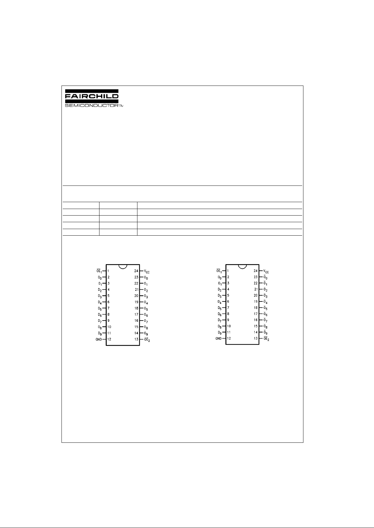
Connection Diagrams
74F827 74F828
Order Number Package Number Package Description
74F827SC M24B 24-Lead Small Outline Integrated Circuit (SOIC), JEDEC MS-013, 0.300 Wide
74F827SPC N24C 24-Lead Plastic Dual-In-Line Package (PDIP), JEDEC MS-100, 0.300 Wide
74F828SC M24B 24-Lead Small Outline Integrated Circuit (SOIC), JEDEC MS-013, 0.300 Wide
74F828SPC N24C 24-Lead Plastic Dual-In-Line Package (PDIP), JEDEC MS-100, 0.300 Wide
Page 2
www.fairchildsemi.com 2
74F827 • 74F828
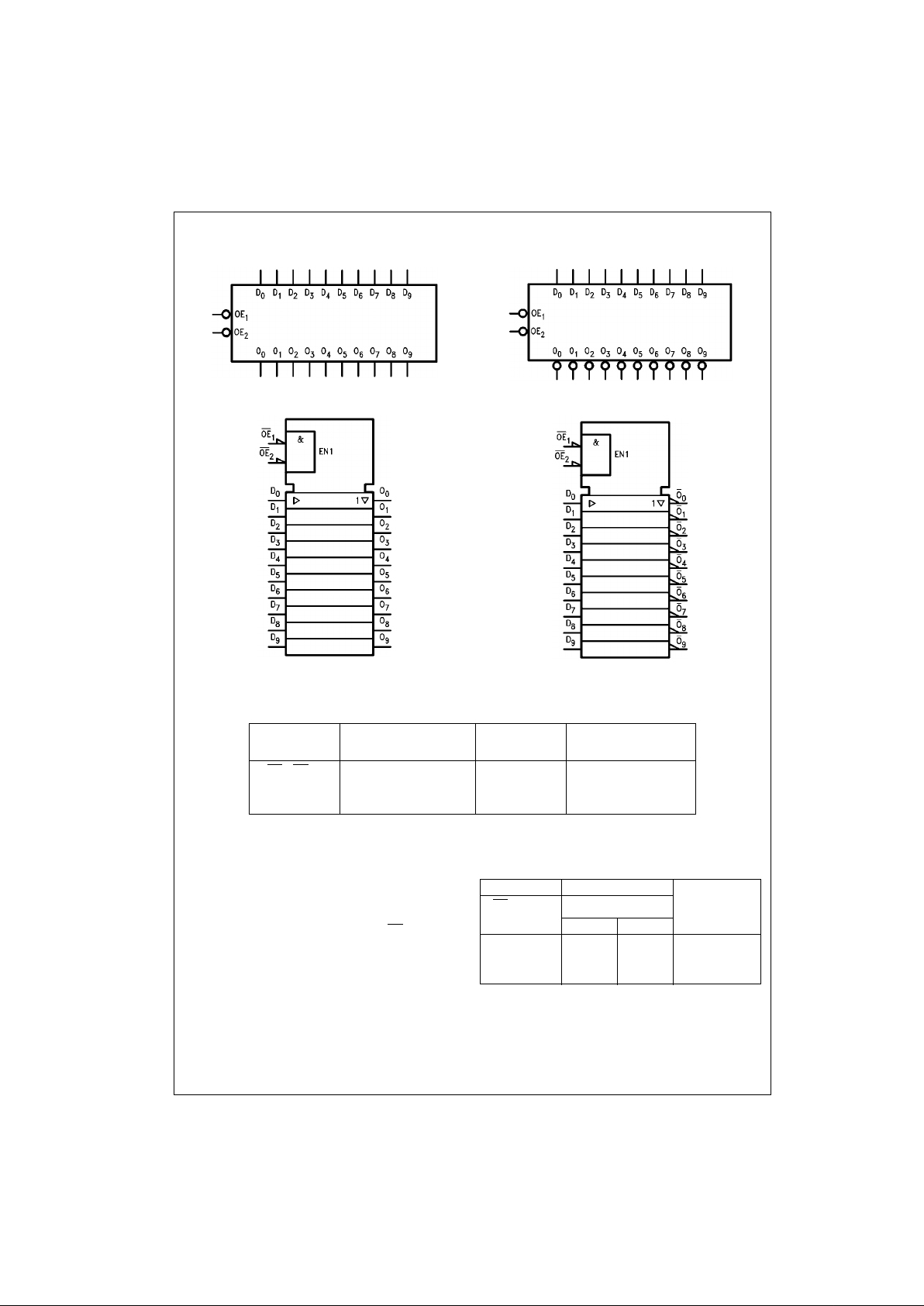
Logic Symbols
74F827
IEEE/IEC
74F827
74F828
IEEE/IEC
74F828
Unit Loading/Fan Out
Functional Description
The 74F827 and 7 4F828 are line drivers designed to be
employed as memory address drivers, clock drivers and
bus-oriented transmitters/receivers which provide
improved PC board de nsity. The devices have 3-STATE
outputs controlled by the Output Enable (OE
) pins. The
outputs can sink 64 mA and source 15 mA. Input clamp
diodes limit high-speed termination effects.
Function Table
H = HIGH Voltage level
L = LOW Voltage Level
Z = High Impedance
X = Immaterial
Pin Names Description
U.L.
Input I
IH/IIL
HIGH/LOW
Output I
OH/IOL
OE1, OE
2
Output Enable Input 1.0/1.0 20 µA/−0.6 mA
D
0–D7
Data Inputs 1.0/1.0 20 µA/−0.6 mA
O
0–O7
Data Outputs, 3-STATE 600/106.6 (80) −12 mA/64 mA (48 mA)
Inputs Outputs
OE
D
n
O
n
Function
74F827 74F828
L H H L Transparent
L L L H Transparent
H X Z Z High Z
Page 3
3 www.fairchildsemi.com
74F827 • 74F828
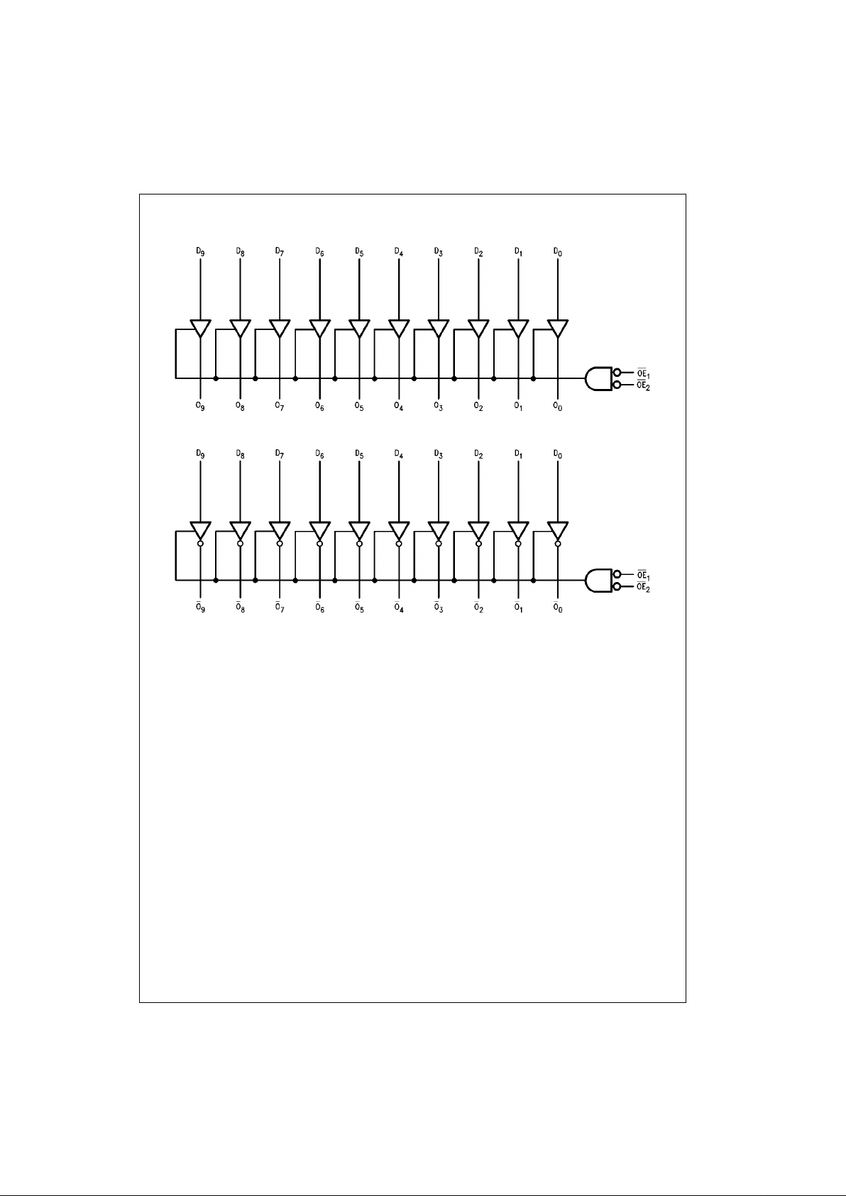
Logic Diagrams
74F827
Please note that this d iagram is provided only f or t he understanding of lo gic operations and should not be used to estimat e propagation delays.
74F828
Please note that this d iagram is provided only f or t he understanding of lo gic operations and should not be used to estimat e propagation delays.
Page 4

www.fairchildsemi.com 4
74F827 • 74F828
Absolute Maximum Ratings(Note 1) Recommended Operating
Conditions
Note 1: Absolute maximum ratings are values beyond which the device
may be damaged or have its useful life impaired. Functional operation
under these conditi ons is not implied.
Note 2: Either voltage limit or curren t limit is sufficient to protect in put s .
DC Electrical Characteristics
Storage Temperature −65°C to +150°C
Ambient Temperature under Bias −55°C to +125°C
Junction Temperature under Bias −55°C to +150°C
V
CC
Pin Potential to Ground Pin −0.5V to +7.0V
Input Voltage (Note 2) −0.5V to +7.0V
Input Current (Note 2) −30 mA to +5.0 mA
Voltage Applied to Output
in HIGH State (with V
CC
= 0V)
Standard Output −0.5V to V
CC
3-STATE Output −0.5V to +5.5V
Current Applied to Output
in LOW State (Max) twice the rated I
OL
(mA)
Free Air Ambient Temperature 0°C to +70°C
Supply Voltage +4.5V to +5.5V
Symbol Parameter Min Typ Max Units
V
CC
Conditions
V
IH
Input HIGH Voltage 2.0 V Recognized as a HIGH Signal
V
IL
Input LOW Voltage 0.8 V Recognized as a LOW Signal
V
CD
Input Clamp Diode Voltage −1.2 V Min IIN = −18 mA
V
OH
Output HIGH 10% V
CC
2.4
VMin
IOH = −3 mA
Voltage 10% V
CC
2.0 IOH = −15 mA
5% V
CC
2.7 IOH = −3 mA
V
OL
Output LOW
10% V
CC
0.55 V Min IOL = 64 mA
Voltage
I
IH
Input HIGH
5.0 µAMaxVIN = 2.7V
Current
I
BVI
Input HIGH Current
7.0 µAMaxVIN = 7.0V
Breakdown Test
I
CEX
Output HIGH
50 µAMaxV
OUT
= V
CC
Leakage Current
V
ID
Input Leakage
4.75 V 0.0
IID = 1.9 µA
Test All Other Pins Grounded
I
OD
Output Leakage
3.75 µA0.0
V
IOD
= 150 mV
Circuit Current All Other Pins Grounded
I
IL
Input LOW Current −0.6 mA Max VIN = 0.5V
I
OZH
Output Leakage Current 50 µAMaxV
OUT
= 2.7V
I
OZL
Output Leakage Current −50 µAMaxV
OUT
= 0.5V
I
OS
Output Short-Circuit Current −100 −225 mA Max V
OUT
= 0V
I
ZZ
Bus Drainage Test 500 µA0.0VV
OUT
= 5.25V
I
CCH
Power Supply Current (74F827) 30 45 mA Max VO = HIGH
I
CCL
Power Supply Current (74F827) 60 90 mA Max VO = LOW
I
CCZ
Power Supply Current (74F827) 40 60 mA Max VO = HIGH Z
I
CCH
Power Supply Current (74F828) 14 20 mA Max VO = HIGH
I
CCL
Power Supply Current (74F828) 56 85 mA Max VO = LOW
I
CCZ
Power Supply Current (74F828) 35 50 mA Max VO = HIGH Z
Page 5

5 www.fairchildsemi.com
74F827 • 74F828
AC Electrical Characteristics
Symbol Parameter
TA = +25°CT
A
= −55°C to +125°CTA = 0°C to +70°C
Units
VCC = +5.0V VCC = +5.0V VCC = +5.0V
CL = 50 pF CL = 50 pF CL = 50 pF
Min Typ Max Min Max Min Max
t
PLH
Propagation Delay 1.0 3.0 5.5 1.0 7.5 1.0 6.5
ns
t
PHL
Data to Output (74F827) 1.5 3.3 5.5 1.5 7.0 1.5 6.0
t
PLH
Propagation Delay 1.0 3.0 5.0 1.0 5.5
ns
t
PHL
Data to Output (74F828) 1.0 2.0 4.0 1.0 4.0
t
PZH
Output Enable Time 3.0 5.7 9.0 2.5 10.0 2.5 9.5
ns
t
PZL
OE to O
n
3.5 6.8 11.5 3.0 12.5 3.0 12.0
t
PHZ
Output Disable Time 1.5 3.3 8.0 1.5 9.0 1.5 8.5
ns
t
PLZ
OE to O
n
1.0 3.5 8.0 1.0 9.0 1.0 8.5
Page 6

www.fairchildsemi.com 6
74F827 • 74F828
Physical Dimensions inches (millimeters) unless otherwise noted
24-Lead Small Outline Integrated Circuit (SOIC), JEDEC MS-013, 0.300 Wide
Package Number M24B
Page 7

7 www.fairchildsemi.com
74F827 • 74F828 10-Bit Buffers/Line Drivers
Physical Dimensions inches (millimeters) unless otherwise noted (Continued)
24-Lead Plastic Dual-In-Line Package (PDIP), JEDEC MS-100, 0.300 Wide
Package Number N24C
Fairchild does not assume any responsibility for use of any circu itry described, no circuit patent license s are implied and
Fairchild reserves the right at any time without notice to change said circuitry and specifications.
LIFE SUPPORT POLICY
FAIRCHILD’S PRODUCTS ARE NOT AUTHORIZED FOR USE AS CRITICAL COMPONENTS IN LIFE SUPPORT
DEVICES OR SYSTEMS WITHOUT THE EXPRESS WRITTEN APPROVAL OF THE PRESIDENT OF FAIRCHILD
SEMICONDUCTOR CORPORATION. As used herein:
1. Life support devices or systems are dev ic es or syste ms
which, (a) are intended for surgical implant into the
body, or (b) support or sustain life, and (c) whose failure
to perform when properly used in accordance with
instructions for use provided i n the labe li ng, can be re asonably expected to result in a significant injury to the
user.
2. A critical componen t in any com ponent o f a l ife supp ort
device or system whose failu re to perform can b e reasonably expected to c ause th e fa i lure of the li fe s upp or t
device or system, or to affect its safety or effectiveness.
www.fairchildsemi.com
 Loading...