

Page 1
© 1999 Fairchild Semiconductor Corporation DS009597 www.fairchildsemi.com
April 1988
Revised August 1999
74F825 8-Bit D-Type Flip-Flop
74F825
8-Bit D-Type Flip-Flop
General Description
The 74F825 is an 8-bit buffered register. It has Clock
Enable and Clear features which are ideal for parity bus
interfacing in high performance microprogramming systems. Also included in the 74F825 are multiple enables that
allow multi-user control of the interface.
Features
■ 3-STATE output
■ Clock enab le and clear
■ Multiple output enables
Ordering Code:
Devices also availab le in Tape and Reel. Specify by appending th e s uffix let t er “X” to the ordering code.
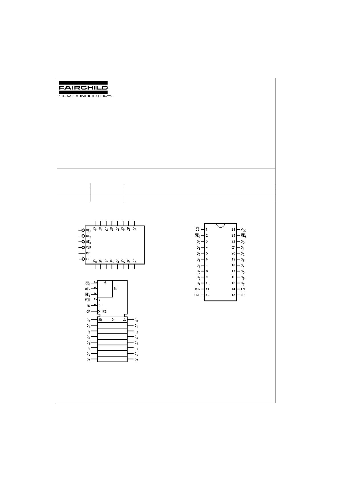
Logic Symbols
IEEE/IEC
Connection Diagram
Order Number Package Number Package Description
74F825SC M24B 24-Lead Small Outline Integrated Circuit (SOIC), JEDEC MS-013, 0.300 Wide
74F825SPC N24C 24-Lead Plastic Dual-In-Line Package (PDIP), JEDEC MS-100, 0.300 Wide
Page 2
www.fairchildsemi.com 2
74F825
Unit Loading/Fan Out
Functional Description
The 74F825 consis ts of eight D-type edge-triggered f lipflops. This device h as 3-STATE true outputs and is orga nized in broadside pinning. In addition to the clock and output enable pins, the buffered clock (CP) and buffered
Output Enable (OE
) are common to all flip-flops. The flipflops will store the state of their individual D inputs that
meet the setup and ho ld times requi rements on the L OWto-HIGH CP transition. With the OE
LOW the contents of
the flip-flops are av ailable at the outputs. W hen the OE
is
HIGH, the outputs go to th e high impeda nce state. Op eration of the OE
input does not affect t he state of the flip-
flops. The 74F825 has Clea r (CLR
) and Clock Enable (EN)
pins.
When the CLR
is LOW and the OE is LOW the outputs are
LOW. When CLR
is HIGH, data can be entered into the flip-
flops. When EN
is LOW, data on the inputs is transferred to
the outputs on the LOW-to-HIGH clock transition . When
the EN
is HIGH the outputs do not ch ange state, regard-
less of the data or clock input transitions.
Function Table
L = LOW Voltage Level Z = High Impedance
H = HIGH Voltage Level
= LOW-to-HIGH Transition
X = Immaterial NC = No Change
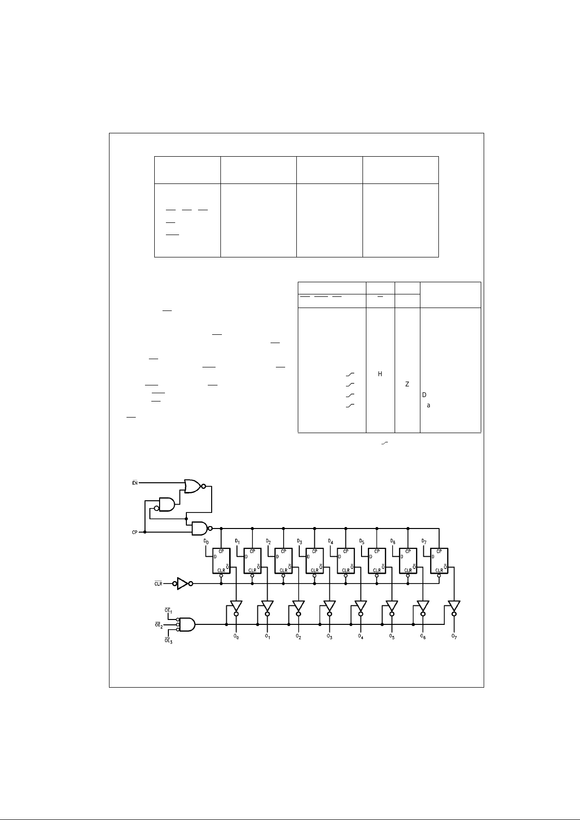
Logic Diagram
Please note that this diagram is provided o nly f or t he understanding of lo gic operations and should not be used to estimate propagation delays.
Pin Names Description
U.L.
Input I
IH/IIL
HIGH/LOW
Output I
OH/IOL
D0–D
7
Data Inputs 1.0/1.0 20 µA/−0.6 mA
O
0–O7
3-STATE Data Outputs 150/40 (33.3) −3 mA/24 mA (20 mA)
OE
1
, OE2, OE
3
Output Enable Input 1.0/1.0 20 µA/−0.6 mA
EN
Clock Enable 1.0/1.0 20 µA/−0.6 mA
CLR
Clear 1.0/1.0 20 µA/−0.6 mA
CP Clock Input 1.0/2.0 20 µA/−1.2 mA
Inputs Internal Output
Function
OE
CLR EN CP D Q O
HHLHXNC ZHold
HHLLXNC ZHold
H H H X X NC Z Hold
LHHXXNC NCHold
H L X X X H Z Clear
L L X X X H L Clear
HHL
L H Z Load
HHL
H L Z Load
LHL
L H L Data Available
LHL
H L H Data Available
L H L H X NC NC No Change in Data
L H L L X NC NC No Change in Data
Page 3

3 www.fairchildsemi.com
74F825
Absolute Maximum Ratings(Note 1) Recommended Operating
Conditions
Note 1: Absolute maximum ratings are values beyon d which the device
may be damaged or have its useful life impaired . Functional operation
under these condit ions is not implied.
Note 2: Either voltage limit or curren t limit is sufficient to protect in puts.
DC Electrical Characteristics
Storage Temperature −65°C to +150°C
Ambient Temperature under Bias −55°C to +125°C
Junction Temperature under Bias −55°C to +150°C
V
CC
Pin Potential to Ground Pin −0.5V to +7.0V
Input Voltage (Note 2) −0.5V to +7.0V
Input Current (Note 2) −30 mA to +5.0 mA
Voltage Applied to Output
in HIGH State (with V
CC
= 0V)
Standard Output −0.5V to V
CC
3-STATE Output −0.5V to +5.5V
Current Applied to Output
in LOW State (Max) twice the rated I
OL
(mA)
Free Air Ambi ent Temperature 0°C to +70°C
Supply Voltage +4.5V to +5.5V
Symbol Parameter Min Typ Max Units
V
CC
Conditions
V
IH
Input HIGH Voltage 2.0 V Recognized as a HIGH Signal
V
IL
Input LOW Voltage 0.8 V Recognized as a LOW Signal
V
CD
Input Clamp Diode Voltage −1.2 V Min IIN = −18 mA
V
OH
Output HIGH 10% V
CC
2.5
VMin
IOH = −1 mA
Voltage 10% V
CC
2.4 IOH = −3 mA
5% V
CC
2.7 IOH = −1 mA
5% V
CC
2.7 IOH = −3 mA
V
OL
Output LOW
10% V
CC
0.5 V Min IOL = 24 mA
Voltage
I
IH
Input HIGH
5.0 µAMaxVIN = 2.7V
Current
I
BVI
Input HIGH Current
7.0 µAMaxVIN = 7.0V
Breakdown Test
I
CEX
Output HIGH
50 µAMaxV
OUT
= V
CC
Leakage Current
V
ID
Input Leakage
4.75 V 0.0
IID = 1.9 µA
Test All Other Pins Grounded
I
OD
Output Leakage
3.75 µA0.0
V
IOD
= 150 mV
Circuit Current All Other Pins Grounded
I
IL
Input LOW Current −0.6 mA Max VIN = 0.5V
I
OZH
Output Leakage Current 50 µAMaxV
OUT
= 2.7V
I
OZL
Output Leakage Current −50 µAMaxV
OUT
= 0.5V
I
OS
Output Short-Circuit Current −60 −150 mA Max V
OUT
= 0V
I
ZZ
Buss Drainage Test 500 µA0.0VV
OUT
= 5.25V
I
CCZ
Power Supply Current 75 90 mA Max VO = HIGH Z
Page 4

www.fairchildsemi.com 4
74F825
AC Electrical Characteristics
AC Operating Requirements
Symbol Parameter
TA = +25°CT
A
= −55°C to +125°CTA = 0°C to +70°C
Units
VCC = +5.0V VCC = +5.0V VCC = +5.0V
CL = 50 pF CL = 50 pF CL = 50 pF
Min Typ Max Min Max Min Max
f
MAX
Maximum Clock Frequency 100 160 60 70 MHz
t
PLH
Propagation Delay 2.0 6.5 9.5 2.0 10.5 2.0 10.5
ns
t
PHL
CP to O
n
2.0 6.6 9.5 2.0 10.5 2.0 10.5
t
PHL
Propagation Delay
4.0 7.4 12.0 4.0 13.0 4.0 13.0 ns
CLR to O
n
t
PZH
Output Enable Time 2.0 6.5 10.5 2.0 13.0 2.0 11.5
t
PZL
OE to O
n
2.0 6.6 10.5 2.0 13.0 2.0 11.5
ns
t
PHZ
Output Disable TIme 1.5 3.5 7.0 1.0 7.5 1.5 7.5
t
PLZ
OE to O
n
1.53.37.01.07.51.57.5
Symbol Parameter
TA = +25°CTA = −55°C to +125°CTA = 0°C to +70°C
UnitsVCC = +5.0V VCC = +5.0V VCC = +5.0V
Min Max Min Max Min Max
tS(H) Setup Time, HIGH or LOW 2.5 4.0 3.0
tS(L) Dn to CP 2.5 4.0 3.0
ns
tH(H) Hold Time, HIGH or LOW 2.5 2.5 2.5
tH(L) Dn to CP 2.5 2.5 2.5
tS(H) Setup Time, HIGH or LOW 4.5 5.0 5.0
tS(L)
EN to CP
2.5 3.0 3.0
ns
tH(H) Hold Time, HIGH or LOW 2.0 3.0 1.0
tH(L)
EN to CP
02.00
tW(H) CP Pulse Width 5.0 6.0 6.0
ns
tW(L) HIGH or LOW 5.0 6.0 6.0
tW(L)
CLR Pulse Width, LOW
5.0 5.0 5.0 ns
t
REC CLR Recovery Time
5.0 5.0 5.0 ns
Page 5

5 www.fairchildsemi.com
74F825
Physical Dimensions inches (millimeters) unless otherwise noted
24-Lead Small Outline Integrated Circuit (SOIC), JEDEC MS-013, 0.300 Wide
Package Number M24B
Page 6

www.fairchildsemi.com 6
74F825 8-Bit D-Type Flip-Flop
Physical Dimensions inches (millimeters) unless otherwise noted (Continued)
24-Lead Plastic Dual-In-Line Package (PDIP), JEDEC MS-100, 0.300 Wide
Package Number N24C
Fairchild does not assume any responsibility for use of any circuitry described, no circuit pate nt licenses are implied and
Fairchild reserves the right at any time without notice to change said circuitry and specifications.
LIFE SUPPORT POLICY
FAIRCHILD’S PRODUCTS ARE NOT AUTHORIZED FOR USE AS CRITICAL COMPONENTS IN LIFE SUPPORT
DEVICES OR SYSTEMS WITHOUT THE EXPRESS WRITTEN APPROVAL OF THE PRESIDENT OF FAIRCHILD
SEMICONDUCTOR CORPORATION. As used herein:
1. Life support de vices o r systems a re devices or syste ms
which, (a) are intended for surgical implant into the
body, or (b) support or sustain life, and (c) whose failure
to perform when properly used in accordance with
instructions for use provided in the labeling, can be reasonably expected to result in a significant inju ry to the
user.
2. A critical com ponent in any com ponen t of a life supp ort
device or system whose failu re to perform can be reasonably expected to ca use the fa i lure of the life su pp ort
device or system, or to affect its safety or effectiveness.
www.fairchildsemi.com
 Loading...