

Page 1
© 1999 Fairchild Semiconductor Corporation DS009551 www.fairchildsemi.com
April 1988
Revised August 1999
74F538 1-of-8 Decoder with 3-STATE Outputs
74F538
1-of-8 Decoder with 3-STATE Outputs
General Description
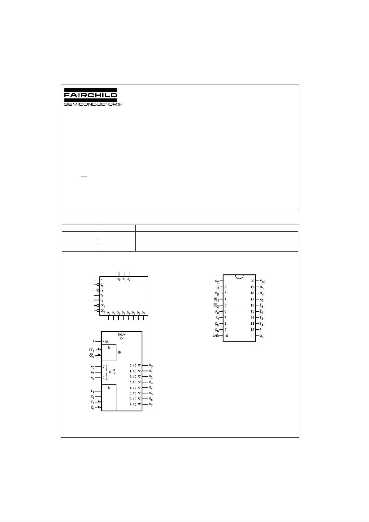
The 74F538 decoder/dem ultiplexer acce pts three Address
(A
0–A2
) input signals and decodes them to select one of
eight mutually exclusive outputs. A polarity control input (P)
determines whether th e outputs are active LOW or active
HIGH. A HIGH Signal on eith er of the active LOW Outp ut
Enable (OE
) inputs forces all output s to the high impedance state. Two active HIGH and two act ive LOW input
enables are available for easy e xpan sion to 1-o f 32 decoding with four packages, o r for data de mul tiplexin g to 1 -of-8
or 1-of-16 destinations.
Features
■ Output polarity control
■ Data demultiplexing capability
■ Multiple enables for expansion
■ 3-STATE outputs
Ordering Code:
Devices also availab le in Tape and Reel. Specify by appending th e s uffix let t er “X” to the ordering code.
Logic Symbols
IEEE/IEC
Connection Diagram
Order Number Package Number Package Description
74F538SC M20B 20-Lead Small Outline Integrated Circuit (SOIC), JEDEC MS-013, 0.300 Wide
74F538SJ M20D 20-Lead Small Outline Package (SOP), EIAJ TYPE II, 5.3mm Wide
74F538PC N20A 20-Lead Plastic Dual-In-Line Package (PDIP), JEDEC MS-001, 0.300 Wide
Page 2
www.fairchildsemi.com 2
74F538
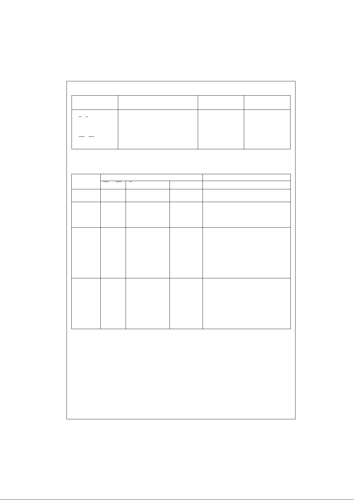
Unit Loading/Fan Out
Truth Table
H = HIGH Voltage Level
L = LOW Voltage Level
X = Immaterial
Z = High Impedance
Pin Names Description
U.L.
Input I
IH/IIL
HIGH/LOW
Output I
OH/IOL
A0–A
2
Address Inputs 1.0/1.0 20 µA/−0.6 mA
E
1
, E
2
Enable Inputs (Active LOW) 1.0/1.0 20 µA/−0.6 mA
E
3
, E
4
Enable Inputs (Active HIGH) 1.0/1.0 20 µA/−0.6 mA
P Polarity Control Input 1.0/1.0 20 µA/−0.6 mA
OE
1
, OE
2
Output Enable Inputs (Active LOW) 1.0/1.0 20 µA/−0.6 mA
O
0–O7
3-STATE Outputs 150/40 (33.3) −3 mA/24 mA (20 mA)
Function
Inputs Outputs
OE
1OE2E1E2E3E4A2A1A0O0O1O2O3O4O5O6O7
High H X XXXXXXXZZZZZZZZ
Impedance X HXXXXXXXZZZZZZZZ
Disable L L HXXXXXX
L L XHXXXXX Outputs Equal P Input
L L XXLXXXX
L L XXXLXXX
Active HIGH L LLLHHLLLHLLLLLLL
Output L L LLHHLLHLHLLLLLL
(P = L) L LLLHHLHLLLHLLLLL
L L LLHHLHHLLLHLLLL
L L LLHHHLLLLLLHLLL
L L LLHH HLHLLLLLHLL
L L LLHHHHLLLLLL LHL
L L LLHHHHHLLLLLLLH
Active LOW L L L LHHL LL LHHHHHHH
Output L L L LHHL LHHLHHHHHH
(P = H) L L LLHHL HLHHLHHHHH
L L L LHHLHHHHHLHHHH
L L LL HHHLLHHHHLHHH
L L L LHHHLHHHHHHLHH
L L L LHHHHLHHHHH HLH
L L L LHHHH HHH HHHHHL
Page 3
3 www.fairchildsemi.com
74F538
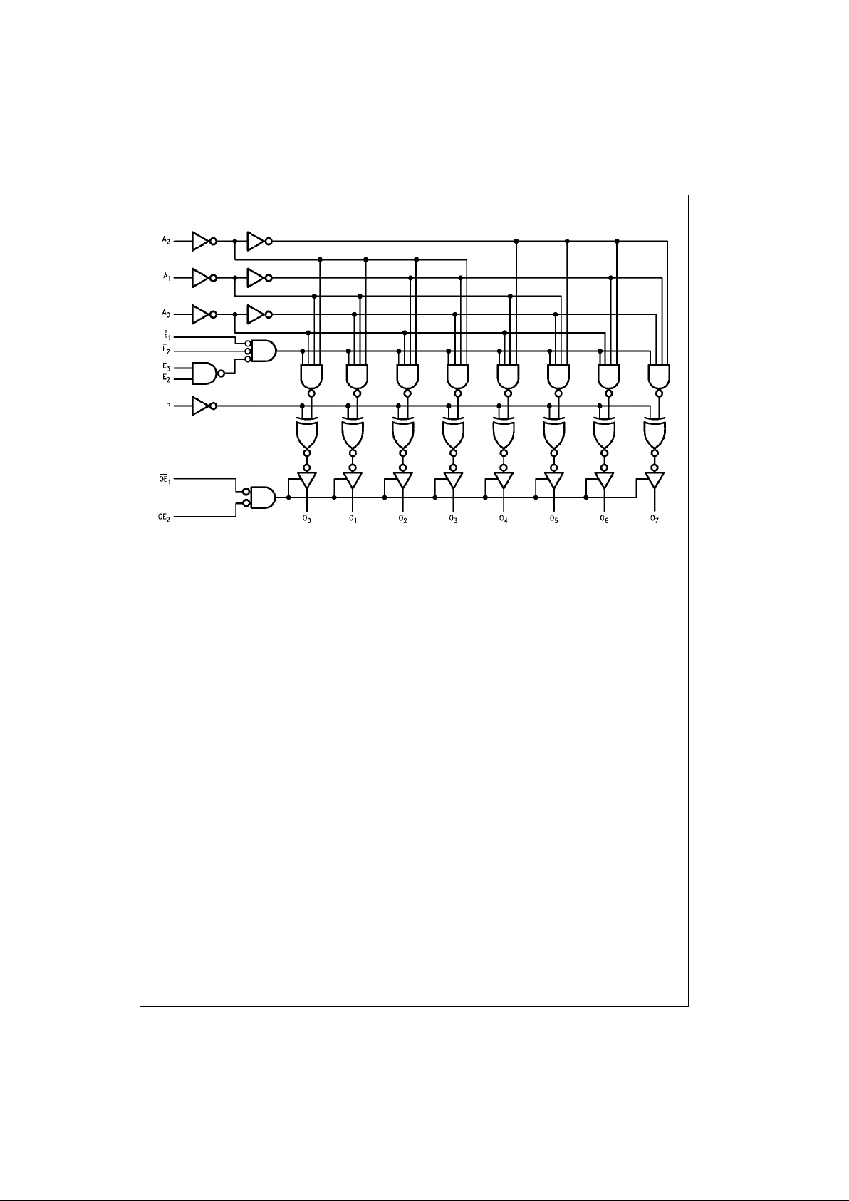
Logic Diagram
Please note that this d iagram is provided only f or t he understanding of lo gic operations and should not be used to estimat e propagation delays.
Page 4

www.fairchildsemi.com 4
74F538
Absolute Maximum Ratings(Note 1) Recommended Operating
Conditions
Note 1: Absolute maximum ratings are values beyond which the device
may be damaged or have its useful life impaired. Functional operation
under these conditi ons is not implied.
Note 2: Either voltage limit or curren t limit is sufficient to protect in put s .
DC Electrical Characteristics
Storage Temperature −65°C to +150°C
Ambient Temperature under Bias −55°C to +125°C
Junction Temperature under Bias −55°C to +150°C
V
CC
Pin Potential to Ground Pin −0.5V to +7.0V
Input Voltage (Note 2) −0.5V to +7.0V
Input Current (Note 2) −30 mA to +5.0 mA
Voltage Applied to Output
in HIGH State (with V
CC
= 0V)
Standard Output −0.5V to V
CC
3-STATE Output −0.5V to +5.5V
Current Applied to Output
in LOW State (Max) twice the rated I
OL
(mA)
Free Air Ambient Temperature 0°C to +70°C
Supply Voltage +4.5V to +5.5V
Symbol Parameter Min Typ Max Units
V
CC
Conditions
V
IH
Input HIGH Voltage 2.0 V Recognized as a HIGH Signal
V
IL
Input LOW Voltage 0.8 V Recognized as a LOW Signal
V
CD
Input Clamp Diode Voltage −1.2 V Min IIN = −18 mA
V
OH
Output HIGH 10% V
CC
2.5
VMin
IOH = −1 mA
Voltage 10% V
CC
2.4 IOH = −3 mA
5% V
CC
2.7 IOH = −1 mA
5% V
CC
2.7 IOH = −3 mA
V
OL
Output LOW
10% V
CC
0.5 V Min IOL = 20 mA
Voltage
I
IH
Input HIGH Current 5.0 µAMaxVIN = 2.7V
I
BVI
Input HIGH Current
7.0 µAMaxVIN = 7.0V
Breakdown Test
I
CEX
Output HIGH
50 µAMaxV
OUT
= V
CC
Leakage Current
V
ID
Input Leakage
4.75 V 0.0
IID = 1.9 µA
Test All Other Pins Grounded
I
OD
Output Leakage
3.75 µA0.0
V
IOD
= 150 mV
Circuit Current All Other Pins Grounded
I
IL
Input LOW Current −0.6 mA Max VIN = 0.5V
I
OZH
Output Leakage Current 50 µAMaxV
OUT
= 2.7V
I
OZL
Output Leakage Current −50 µAMaxV
OUT
= 0.5V
I
OS
Output Short-Circuit Current −60 −150 mA Max V
OUT
= 0V
I
ZZ
Bus Drainage Test 500 µA0.0VV
OUT
= 5.25V
I
CCH
Power Supply Current 31 45 mA Max VO = HIGH
I
CCL
Power Supply Current 37 56 mA Max VO = LOW
I
CCZ
Power Supply Current 37 56 mA Max VO = HIGH Z
Page 5

5 www.fairchildsemi.com
74F538
AC Electrical Characteristics
Symbol Parameter
TA = +25°CT
A
= 0°C to +70°C
Units
VCC = +5.0V VCC = +5.0V
CL = 50 pF CL = 50 pF
Min Typ Max Min Max
t
PLH
Propagation Delay 6.0 11.0 16.0 6.0 17.0
ns
t
PHL
An to O
n
4.0 7.5 11.0 4.0 12.0
t
PLH
Propagation Delay 5.0 8.5 15.0 5.0 16.0
t
PHL
E1 or E2 to O
n
4.0 6.5 9.0 4.0 10.0
t
PLH
Propagation Delay 6.0 11.0 16.0 6.0 17.0
ns
t
PHL
E3 or E4 to O
n
5.0 10.0 14.0 5.0 15.0
t
PLH
Propagation Delay 6.0 11.5 18.0 6.0 20.0
t
PHL
P to O
n
6.0 11.0 16.0 6.0 17.0
t
PZH
Output Enable Time 3.0 5.5 10.0 3.0 11.0
ns
t
PZL
OE1 or OE2 to O
n
5.0 9.0 13.0 5.0 14.0
t
PHZ
Output Disable Time 2.0 4.0 6.0 2.0 7.0
t
PLZ
OE1 or OE2 to O
n
3.05.08.03.09.0
Page 6

www.fairchildsemi.com 6
74F538
Physical Dimensions inches (millimeters) unless otherwise noted
20-Lead Small Outline Integrated Circuit (SOIC), JEDEC MS-013, 0.300 Wide
Package Number M20B
20-Lead Small Outline Package (SOP), EIAJ TYPE II, 5.3mm Wide
Package Number M20D
Page 7

7 www.fairchildsemi.com
74F538 1-of-8 Decoder with 3-STATE Outputs
Physical Dimensions inches (millimeters) unless otherwise noted (Continued)
20-Lead Plastic Dual-In-Line Package (PDIP), JEDEC MS-001, 0.300 Wide
Package Number N20A
Fairchild does not assume any responsibility for use of any circu itry described, no circuit patent license s are implied and
Fairchild reserves the right at any time without notice to change said circuitry and specifications.
LIFE SUPPORT POLICY
FAIRCHILD’S PRODUCTS ARE NOT AUTHORIZED FOR USE AS CRITICAL COMPONENTS IN LIFE SUPPORT
DEVICES OR SYSTEMS WITHOUT THE EXPRESS WRITTEN APPROVAL OF THE PRESIDENT OF FAIRCHILD
SEMICONDUCTOR CORPORATION. As used herein:
1. Life support de vices o r syst ems are dev ic es or syste ms
which, (a) are intended for surgical implant into the
body, or (b) support or sustain life, and (c) whose failure
to perform when properly used in accordance with
instructions for use provided i n the labe li ng, can be re asonably expected to result in a significant injury to the
user.
2. A critica l compo nent in any com ponen t of a life s uppor t
device or system whose failu re to perform can b e reasonably expected to c ause th e fa i lure of the li fe s upp or t
device or system, or to affect its safety or effectiveness.
www.fairchildsemi.com
 Loading...