

Page 1
© 1999 Fairchild Semiconductor Corporation DS009546 www.fairchildsemi.com
April 1988
Revised August 1999
74F524 8-Bit Registered Comparator
74F524
8-Bit Registered Comparator
General Description
The 74F524 is an 8-bit bidirectional register with parallel
input and output p lus serial input and output progressing
from LSB to MSB. A ll data inputs, s erial and paralle l, are
loaded by the rising edge of the input clock. The device
functions are controlled by two control lines (S
0
, S1) to execute shift, load, hold and read out.
An 8-bit comparator exam ines the da ta store d in the reg is-
ters and on the data bus. Three true-HIGH, open-c ollector
outputs representing “register equal to bus”, “register
greater than bus” and “register less than bus” are provided.
These outputs can be disabled to the OFF state by the use
of Status Enable ( SE
). A mode control has also been pr ovided to allow twos complement as well as magnitude compare. Linking inputs are provided for expansion to long er
words.
Features
■ 8-Bit bidirectional register with bus-oriented input-output
■ Independent serial input-output to register
■ Register bus comparato r with “equal to”, “greater th an”
and “less than” outputs
■ Cascadable in groups of eight bits
■ Open-collector comparator outputs for AND-wired
expansion
■ Twos complement or magnitude compare
Ordering Code:
Devices also availab le in Tape and Reel. Specify by appending th e s uffix let t er “X” to the ordering code.
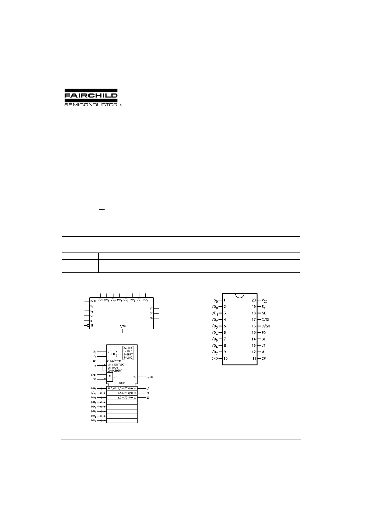
Logic Symbols
IEEE/IEC
Connection Diagram
Order Number Package Number Package Description
74F524SC M20B 20-Lead Small Outline Integrated Circuit (SOIC), JEDEC MS-013, 0.300 Wide
74F524PC N20A 20-Lead Plastic Dual-In-Line Package (PDIP), JEDEC MS-001, 0.300 Wide
Page 2
www.fairchildsemi.com 2
74F524
Unit Loading/Fan Out
Note 1: OC = Open Collector
Number Representation Select Table
Select Truth Table
Status Truth Table
(Hold Mode)
1 = HIGH if data are equal, ot herwise LOW
H = HIGH Voltage Level
L = LOW Voltage Level
X = Immaterial
Pin Names Description
U.L.
Input I
IH/IIL
HIGH/LOW
Output I
OH/IOL
S0, S
1
Mode Select Inputs 1.0/1.0 20 µA/−0.6 mA
C/SI Status Priority or Serial Data Input 1.0/1.0 20 µA/−0.6 mA
CP Clock Pulse Input (Active Rising Edge) 1.0/1.0 20 µA/−0.6 mA
SE
Status Enable Input (Active LOW) 1.0/1.0 20 µA/−0.6 mA
M Compare Mode Select Input 1.0/1.0 20 µA/−0.6 mA
I/O
0
–I/O7Parallel Data Inputs or 3.5/1.083 70 µA/−0.65 mA
3-STATE Parallel Data Outputs 150/40 (33. 3) −3 mA/24 mA (20 mA)
C/SO Status Priority or Serial Data Output 50/33.3 −1 mA/20 mA
LT Register Less Than Bus Output OC (Note 1) /33.3 (Note 1) /20 mA
EQ Register Equal Bus Output OC(Note 1) /33.3 (Note 1) /20 mA
GT Register Greater Than Bus Output OC(Note 1) /33.3 (Note 1) /20 mA
MOperation
L Magnitude Compare
H Twos Complement Compare
S
0
S
1
Operation
L L Hold—Retains Data in Shift Register
L H Read—Read Contents in Register onto Data Bus,
Data Remains in Register Unaffected by Clock
H L Shift—Allows Serial Shifting on Next Rising Clock Edge
H H Load—Load Data on Bus into Register
Inputs Outputs
SE
C/SI Data Comparison EQ GT LT C/SO
HH X HHH1
LL O
A–OH
> I/O0–I/O
7
LHHL
XL O
A–OH
= I/O0–I/O
7
HHHL
HL O
A–OH
< I/O0–I/O
7
LHHL
HH O
A–OH
> I/O0–I/O
7
LHLL
HH O
A–OH
= I/O0–I/O
7
HLLH
LH O
A–OH
< I/O0–I/O
7
LLHL
Page 3
3 www.fairchildsemi.com
74F524
Functional Description
The 74F524 contains eight D-type flip-flops connected as a
shift register with provision for ei ther pa rallel or seri al loading. Parallel data may be read from or loaded into the registers via the data bus I/O
0
–I/O7. Serial data is enter ed fro m
the C/SI input and may be shifted into the register and out
through the C/SO output. Both parallel and serial data entry
occur on the rising edge of the input clock (CP). The operation of the shift reg ister i s cont rolle d by t wo s ignals S
0
and
S
1
according to the Select Truth Table. The 3-STATE parallel output buffers are enabled only in the Read mode.
One port of an 8-bit compara tor is attached to the data bus
while the other port is tied to the outputs of the internal register. Three active-OFF, open-collector outputs indicate
whether the contents held in th e shift register are “great er
than”, (GT), “less than” (LT), or “equal to” (E Q) the dat a on
the input bus. A HI GH signal on the Status Ena ble (SE
)
input disables these outputs to the OFF state. A mode control input (M) allows selection between a straightforward
magnitude compare or a comparison between twos complement numbers.
For “greater than” or “les s than” detection, the C/SI input
must be held HIGH, as indicat ed in the Status Truth Table.
The internal logic is arra nged such that a LOW signal on
the C/SI input disables the “great er than” and “less than”
outputs. The C/SO output will be forced HIGH if the “equal
to” status condition exists, otherwise C/SO will be held
LOW. These facilities enable the 74F524 to be cascaded
for word length greater than eight bits.
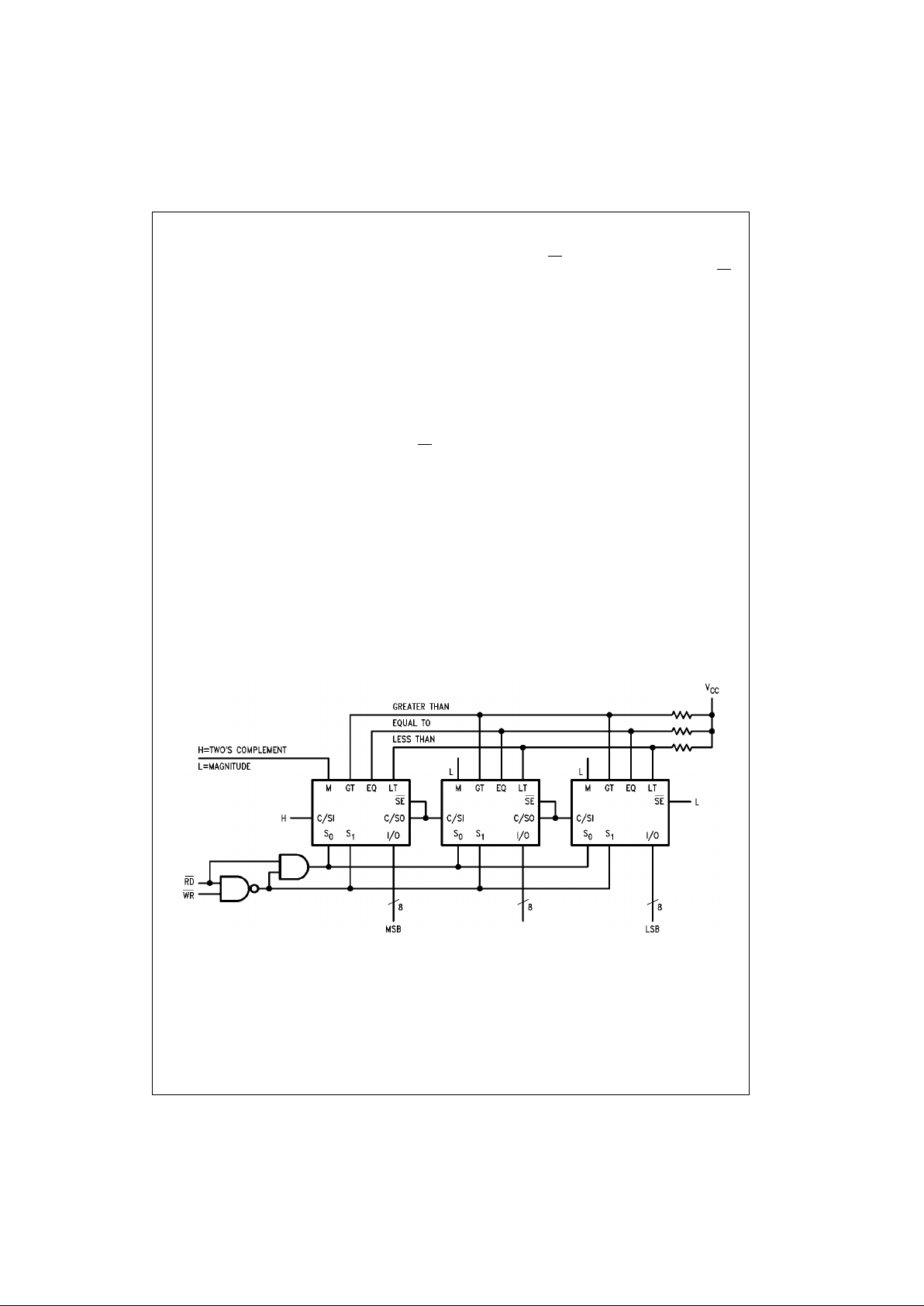
Word length expansion (in groups of eight bits) can be
achieved by connecting the C/SO output of the more signif-
icant byte to the C/SI input of the next less significant byte
and also to its own SE
input (see Figure 1). Th e C /SI i n pu t
of the most significant device is held HI GH while the SE
input of the least significant device is held LOW. The corresponding status outputs are AND-wired together. In the
case of twos complement nu mbe r co mpa re , only th e M ode
input to the most signifi cant device should be HIGH. T he
Mode inputs to all other cascaded devices are held LOW.
Suppose that an inequality condition is detected in the
most significant device. Assu ming that the byte stored in
the register is greater than the byte on the data bus, the EQ
and LT outputs will be pulled LOW and the GT output will
float HIGH. Also the C/SO outp ut of the most significant
device will be forced LOW, disabling the subsequent
devices but enabling its own status outputs. The correct
status condition is thus indicated. The same applies if the
registered byte is less th an th e data byte, only in this case
the EQ and GT outputs go LOW and LT output floats HIGH.
If an equality condi tion is detected in the most significant
device, its C/SO outpu t is forced HIGH. This ena bles the
next less significant device and also disables its own status
outputs. In this way, the status ou tput priority is handed
down to the next less significant device which now effectively becomes the most si gnificant byte. The worst case
propagation delay for a compare operation involving “n”
cascaded 74F524s will be when an equality condition is
detected in all but the least significant byte. In this case, the
status priority has to ripple all the way down the chain
before the correct status outp ut is established. Typically,
this will take 35 + 6(n−2) ns.
Function Diagram
FIGURE 1. Cascading 74F524s for Comparing Longer Words
Page 4

www.fairchildsemi.com 4
74F524
Block Diagram
Notes:
1. 3-ST ATE Output
2. Open-Collector Output
Page 5

5 www.fairchildsemi.com
74F524
Absolute Maximum Ratings(Note 2) Recommended Operating
Conditions
Note 2: Absolute maximum ratings are values beyon d which the device
may be damaged or have its useful life impaired . Functional operation
under these condit ions is not implied.
Note 3: Either voltage limit or curren t limit is sufficient to protect in puts.
DC Electrical Characteristics
Storage Temperature −65°C to +150°C
Ambient Temperature under Bias −55°C to +125°C
Junction Temperature under Bias −55°C to +150C
V
CC
Pin Potential to Ground Pin −0.5V to +7.0V
Input Voltage (Note 3) −0.5V to +7.0V
Input Current (Note 3) −30 mA to +5.0 mA
Voltage Applied to Output
in HIGH State (with V
CC
= 0V)
Standard Output −0.5V to V
CC
3-STATE Output −0.5V to +5.5V
Current Applied to Output
in LOW State (Max) twice the r ated I
OL
(mA)
Free Air Ambi ent Temperat ure 0°C to +70°C
Supply Voltage +4.5V to +5.5V
Symbol Parameter Min Typ Max Units
V
CC
Conditions
V
IH
Input HIGH Voltage 2.0 V Recognized as a HIGH Signal
V
IL
Input LOW Voltage 0.8 V Recognized as a LOW Signal
V
CD
Input Clamp Diode Voltage −1.2 V Min IIN = −18 mA
V
OH
Output HIGH 10% V
CC
2.5
VMin
IOH = −1 mA
Voltage 10% V
CC
2.4 IOH = −3 mA
5% V
CC
2.7 IOH = −1 mA
5% V
CC
2.7 IOH = −3 mA
V
OL
Output LOW 10% V
CC
0.5
VMin
IOL = 20 mA (I/On)
Voltage 10% V
CC
0.5 IOL = 24 mA (LT, GT, EQ, C/SO)
I
IH
Input HIGH Current 5.0 µAMaxVIN = 2.7V
I
BVI
Input HIGH Current
7.0 µAMax
VIN = 7.0V
Breakdown Test
I
CEX
Output HIGH
50 µAMax
V
OUT
= VCC (I/On, C/SO)
Leakage Current
V
ID
Input Leakage
4.75 V 0.0
IID = 1.9 µA
Test All Other Pins Grounded
I
OD
Output Leakage
3.75 µA0.0
V
IOD
= 150 mV
Circuit Current All Other Pins Grounded
I
IL
Input LOW Current −0.6 mA Max VIN = 0.5V
IIH + I
OZH
Output Leakage Current 70 µAMaxV
I/O
= 2.7V
IIL + I
OZL
Output Leakage Current −650 µAMaxV
I/O
= 0.5V
I
OS
Output Short-Circuit Current −60 −150 mA Max V
OUT
= 0V
I
OHC
Open Collector, Output
250 µAMinV
OUT
= V
CC
OFF Leakage Test
I
CCH
Power Supply Current 128 180 mA Max VO = HIGH
I
CCL
Power Supply Current 128 180 mA Max VO = LOW
I
CCZ
Power Supply Current 128 180 mA Max VO = HIGH Z
Page 6

www.fairchildsemi.com 6
74F524
AC Electrical Characteristics
Symbol Parameter
TA = +25°CT
A
= 0°C to +70°C
Units
VCC = +5.0V VCC = +5.0V
CL = 50 pF CL = 50 pF
Min Typ Max Min Max
f
MAX
Maximum Shift Frequency 50 75 50 MHz
t
PLH
Propagation Delay 9.0 16.5 20.0 9.0 21.0
t
PHL
I/On to EQ 5.0 9.5 12.0 5.0 13.0
t
PLH
Propagation Delay 8.5 14.1 19.0 8.5 20.0
ns
t
PHL
I/On to GT 6.5 13.0 16.5 6.5 17.5
t
PLH
Propagation Delay 7.0 15.5 20.0 7.0 21.0
t
PHL
I/On to LT 4.5 10.0 14.0 4.5 15.0
t
PLH
Propagation Delay 8.0 15.2 19.5 8.0 20.5
ns
t
PHL
I/On to C/SO 6.0 12.5 16.0 6.0 17.0
t
PLH
Propagation Delay 10.0 20.0 25.0 10.0 26.0
t
PHL
CP to EQ 4.0 8.5 16.5 4.0 17.5
t
PLH
Propagation Delay 10.0 16.5 21.0 10.0 22.0
ns
t
PHL
CP to GT 8.5 17.0 22.0 8.5 23.0
t
PLH
Propagation Delay 9.0 20.0 25.0 9.0 26.0
t
PHL
CP to LT 5.5 13.5 17.0 5.5 18.0
t
PLH
Propagation Delay
8.5 16.5 21.0 8.5 22.0
CP to C/SO (Load)
ns
t
PLH
Propagation Delay 5.0 10.0 13.0 5.0 14.0
t
PHL
CP to C/SO (Serial Shift) 4.5 9.0 11.5 4.5 12.5
t
PLH
Propagation Delay 9.0 15.0 19.0 9.0 20.0
t
PHL
C/SI to GT 3.0 6.5 8.5 3.0 9.5
ns
t
PLH
Propagation Delay 8.0 15.5 20.0 8.0 21.0
t
PHL
C/SI to LT 3.5 6.5 8.5 3.5 9.5
t
PLH
Propagation Delay 6.5 11.5 14.5 6.5 15.5
ns
t
PHL
S0, S1 to C/SO 5.5 14.0 18.0 5.5 19.0
t
PLH
Propagation Delay 3.5 8.0 10.5 3.5 11.5
t
PHL
SE to EQ
2.5 6.0 8.0 2.5 9.0
t
PLH
Propagation Delay 6.5 12.5 16.0 6.5 17.0
ns
t
PHL
SE to GT
3.5 6.0 8.0 3.5 9.0
t
PLH
Propagation Delay 5.0 10.5 13.5 5.0 14.5
t
PHL
SE to LT
3.5 6.0 8.0 3.5 9.0
t
PLH
Propagation Delay 4.0 8.5 11.0 4.0 12.0
ns
t
PHL
C/SI to C/SO 4.0 8.5 11.0 4.0 12.0
t
PLH
Propagation Delay 8.0 15.0 19.5 8.0 20.5
t
PHL
M to GT 6.0 12.0 17.5 6.0 18.5
ns
t
PLH
Propagation Delay 8.0 17.0 22.0 8.0 23.0
t
PHL
M to LT 4.5 9.5 12.0 4.5 13.0
t
PLH
Propagation Delay 15.0 25.0 33.0 15.0 35.0
t
PHL
S0, S1 to EQ 9.0 15.0 19.0 9.0 20.0
t
PLH
Propagation Delay 10.5 18.0 23.0 10.5 24.0
ns
t
PHL
S0, S1 to GT 10.5 18.0 23.0 10.5 24.0
t
PLH
Propagation Delay 13.0 22.0 28.0 13.0 30.0
t
PHL
S0, S1 to LT 12.0 19.0 24.0 12.0 25.0
t
PZH
Output Enable Time 4.5 10.0 13.0 4.5 14.0
ns
t
PZL
S0, S1 to I/O
n
5.5 11.0 15.0 5.5 16.0
t
PHZ
Output Disable Time 3.5 8.0 12.0 3.5 13.0
t
PLZ
S0, S1 to I/O
n
4.5 9.6 12.5 4.5 13.5
Page 7

7 www.fairchildsemi.com
74F524
AC Operating Requirements
Symbol Parameter
TA = +25°CT
A
= 0°C to +70°C
UnitsVCC = +5.0V VCC = +5.0V
Min Max Min Max
tS(H) Setup Time, HIGH or LOW 6.0 6.0
tS(L) I/On to CP 6.0 6.0
ns
tH(H) Hold Time, HIGH or LOW 0 0
tH(L) I/On to CP 0 0
tS(H) Setup Time, HIGH or LOW 10.0 10.0
tS(L) S0 or S1 to CP 10.0 10.0
ns
tH(H) Hold Time, HIGH or LOW 0 0
tH(L) S0 or S1 to CP 0 0
tS(H) Setup Time, HIGH or LOW 7.0 7.0
tS(L) C/SI to CP 7.0 7.0
ns
tH(H) Hold Time, HIGH or LOW 0 0
tH(L) C/SI to CP 0 0
tW(H) Clock Pulse Width, HIGH 5.0 5.0 ns
Page 8

www.fairchildsemi.com 8
74F524
Physical Dimensions inches (millimeters) unless otherwise noted
20-Lead Small Outline Integrated Circuit (SOIC), JEDEC MS-013, 0.300 Wide
Package Number M20B
Page 9

9 www.fairchildsemi.com
74F524 8-Bit Registered Comparator
Physical Dimensions inches (millimeters) unless otherwise noted (Continued)
20-Lead Plastic Dual-In-Line Package (PDIP), JEDEC MS-001, 0.300 Wide
Package Number N20A
Fairchild does not assume any responsibility for use of any circu itry described, no circuit patent license s are implied and
Fairchild reserves the right at any time without notice to change said circuitry and specifications.
LIFE SUPPORT POLICY
FAIRCHILD’S PRODUCTS ARE NOT AUTHORIZED FOR USE AS CRITICAL COMPONENTS IN LIFE SUPPORT
DEVICES OR SYSTEMS WITHOUT THE EXPRESS WRITTEN APPROVAL OF THE PRESIDENT OF FAIRCHILD
SEMICONDUCTOR CORPORATION. As used herein:
1. Life support devices or systems are dev ic es or syste ms
which, (a) are intended for surgical implant into the
body, or (b) support or sustain life, and (c) whose failure
to perform when properly used in accordance with
instructions for use provided i n the labe li ng, can be re asonably expected to result in a significant injury to the
user.
2. A critical componen t in any com ponent o f a l ife supp ort
device or system whose failu re to perform can b e reasonably expected to c ause th e fa i lure of the li fe s upp or t
device or system, or to affect its safety or effectiveness.
www.fairchildsemi.com
 Loading...