

Page 1
查询N74456D供应商
INTEGRATED CIRCUITS
74F455*, 74F456
Buffers/drivers
* Discontinued part. Please see the Discontinued Product List.
Product specification
Supersedes data of 1990 Nov 26
IC15 Data Handbook
1999 Jan 08
Page 2
Philips Semiconductors Product specification
74F455,* 74F456Buffers/Drivers
74F455 Octal Buffer/Driver with Parity, Inverting (3-State)
74F456 Octal Buffer/Driver with Parity, Non-Inverting (3-State)
FEATURES
•High impedance NPN base inputs for reduced loading
(40µA in High and Low states)
•74F456 combines 74F244 and 74F280A functions in one package
DESCRIPTION
The 74F455 and 74F456 are octal buffers and line drivers with parity
generation/checking designed to be employed as memory address
drivers, clock drivers and bus-oriented transmitters/receivers. These
parts include parity generator/checker to improve PC board density.
•74F456 is a center pin version of the 74F656A
•74F456 Non-Inverting
TYPE
•3-State outputs sink 64mA and source 15mA
•24-pin plastic Slim DIP (300 mil) package
•Broadside pinout simplifies PC board layout
INPUT AND OUTPUT LOADING AND FAN-OUT TABLE
PINS DESCRIPTION
D0–D7 Data inputs 2.0/0.066 40µA/40µA
PI Parity input 1.0/0.033 20µA/20µA
OE0, OE1 Output Enable inputs (active Low) 1.0/0.033 20µA/20µA
ΣE, ΣO Parity outputs 750/106.7 15mA/64mA
Q0–Q7 Data outputs (75F455) 750/106.7 15mA/64mA
Q0–Q7 Data outputs (75F456) 750/106.7 15mA/64mA
NOTE: One (1.0) FAST Unit Load (U.L.) is defined as 20µA in the High state and 0.6mA in the Low state.
74F455 6.5ns 64mA
74F456 7.5ns 64mA
ORDERING INFORMATION
DESCRIPTION
24-pin plastic Slim
DIP (300mil)
24-pin plastic SOL N74456D SOT137-1
TYPICAL
PROPAGATION
DELA Y
COMMERCIAL
V
CC
T
= 0°C to +70°C
amb
N74456N SOT222-1
74F(U.L.)
HIGH/LOW
TYPICAL SUPPL Y CURRENT
(TOTAL)
RANGE
= 5V ±10%,
PKG DWG #
LOAD VALUE
HIGH/LOW
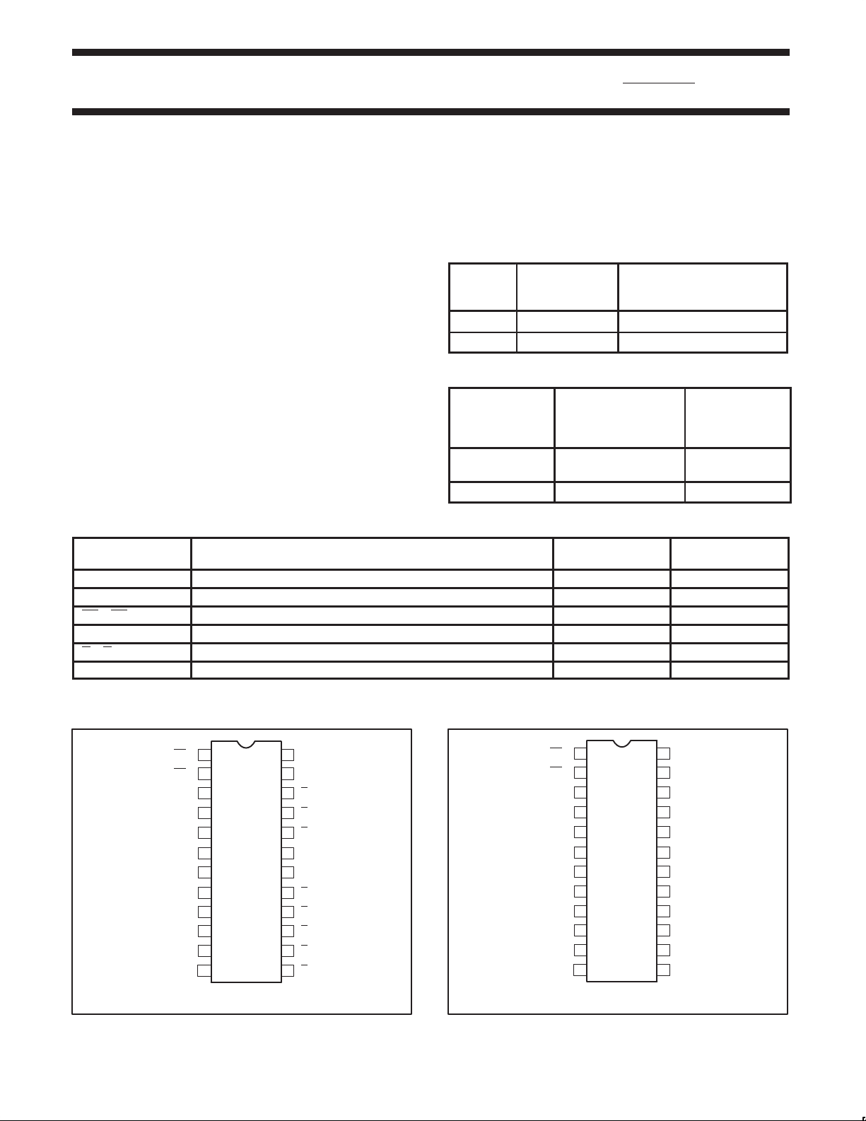
PIN CONFIGURATION – 74F455
0
OE
1
1
OE
2
PI
3
D0
4
D1
5
D2
6
V
7
CC
D3
8
D4
9
D5
10
D6
11
D7 Q
24
23
22
21
20
19
18
17
16
15
14
1312
SF00969
ΣO
ΣE
0
Q
Q
1
2
Q
GND
GND
Q3
Q
4
Q5
6
Q
7
PIN CONFIGURATION – 74F456
0
OE
1
OE
1
2
PI
3
D0
4
D1
5
D2
6
V
7
CC
D3
8
D4
9
D5
10
D6
11
D7 Q7
24
23
22
21
20
19
18
17
16
15
14
1312
SF00958
ΣO
ΣE
Q0
Q1
Q2
GND
GND
Q3
Q4
Q5
Q6
* Discontinued part. Please see the Discontinued Products List.
1999 Jan 08 853–0371 20616
2
Page 3
Philips Semiconductors Product specification
74F455,* 74F456Buffers/Drivers
LOGIC SYMBOL – 74F455
45689101112
D0 D1 D2 D3 D4 D5 D6 D7
3
1
2
VCC= Pin 7
GND = Pin 18, 19
PI
OE0
OE1
Q0 Q1 Q2 Q3 Q4 Q5 Q6 Q7
22 21 20 17 16 15 14 13
LOGIC SYMBOL (IEEE/IEC) – 74F455
3,5,6,7,8
9,10,11,12
1
Z5
Z6
Z7
Z8
Z9
Z10
Z11
Z12
P3
3,5,6,7,8
9,10,11,12
EN4
3
1
2
4
5
6
8
9
10
11
12
2K
[EVEN]
[ODD]
4
SF00961
ΣE
ΣO
23
24
22
21
20
17
16
15
14
13
SF00959
LOGIC SYMBOL – 74F456
45689101112
D0 D1 D2 D3 D4 D5 D6 D7
23
24
3
1
2
VCC= Pin 7
GND = Pin 18, 19
PI
OE0
OE1
Q0 Q1 Q2 Q3 Q4 Q5 Q6 Q7
22 21 20 17 16 15 14 13
ΣE
ΣO
23
24
SF00960
LOGIC SYMBOL (IEEE/IEC) – 74F456
2K
3,5,6,7,8
9,10,11,12
1
Z5
Z6
Z7
Z8
Z9
Z10
Z11
Z12
P3
3,5,6,7,8
9,10,11,12
EN4
3
1
2
4
5
6
8
9
10
11
12
[EVEN]
[ODD]
4
23
24
22
21
20
17
16
15
14
13
SF00962
FUNCTION TABLE
INPUTS
OE0 OE1 Dn Qn Qn
L L L H L
L L H L H
H X X Z Z
X H X Z Z
H = High voltage level
L = Low voltage level
Z = High impedance “off” state
X = Don’t care
* Discontinued part. Please see the Discontinued Products List.
1999 Jan 08
OUTPUTS
74F455 74F456
FUNCTION TABLE for PARITY OUTPUTS
INPUTS OUTPUTS
Number of inputs, High (PI, D0 - D7) ΣE ΣO
Even - 0, 2, 4, 6, 8 H L
Odd - 1, 3, 5, 7, 9 L H
Any OEn = High Z Z
H = High voltage level
L = Low voltage level
Z = High impedance “off” state
X = Don’t care
3
Page 4

Philips Semiconductors Product specification
74F455,* 74F456Buffers/Drivers
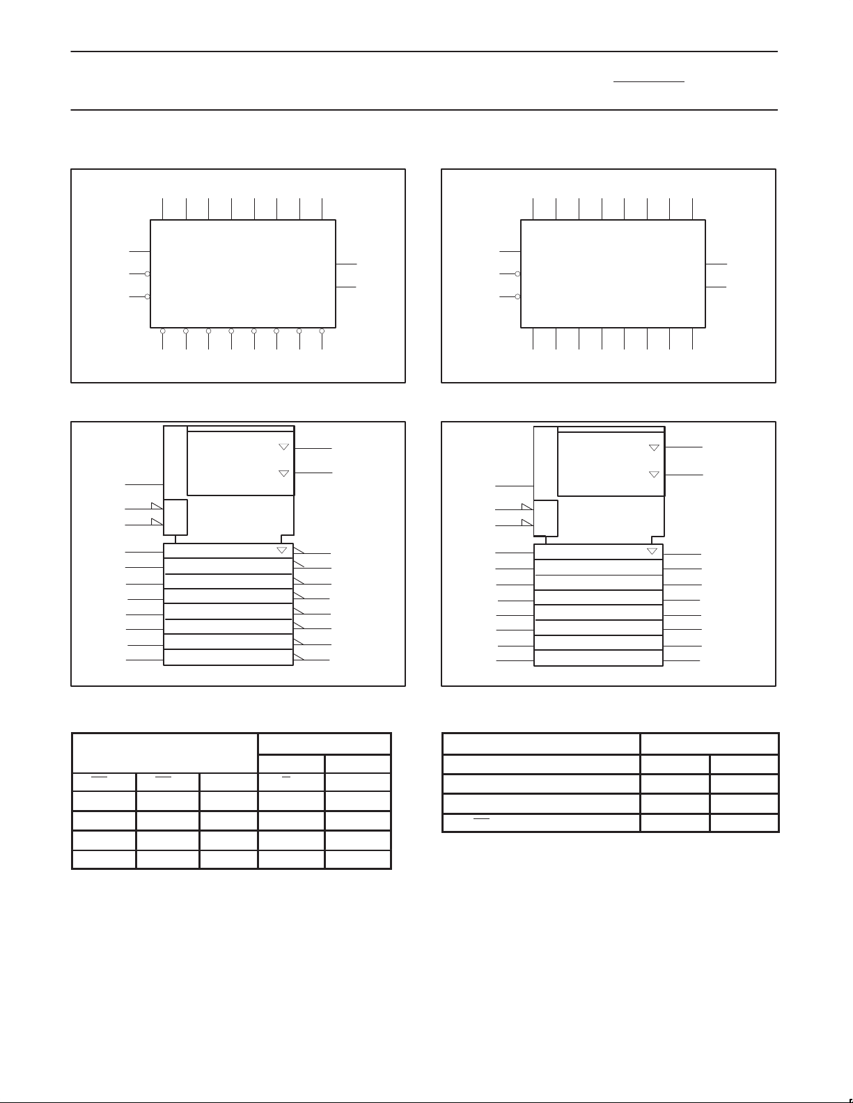
LOGIC DIAGRAM for 74F455
3
PI
23
ΣE
24
ΣO
4
D0
5
D1
6
D2
8
D3
9
D4
22
0
Q
21
1
Q
20
2
Q
17
Q
3
16
Q
4
10
D5
11
D6
12
D7
1
OE
0
2
1
OE
VCC= Pin 7
GND = Pin 18, 19
* Discontinued part. Please see the Discontinued Products List.
1999 Jan 08
15
Q
5
14
6
Q
13
Q
7
SF00963
4
Page 5

Philips Semiconductors Product specification
74F455,* 74F456Buffers/Drivers
LOGIC DIAGRAM for 74F456
3
PI
23
ΣE
24
ΣO
4
D0
5
D1
6
D2
8
D3
9
D4
22
Q0
21
Q1
20
Q2
17
Q3
16
Q4
10
D5
11
D6
12
D7
1
0
OE
2
1
OE
VCC= Pin 7
GND = Pin 18, 19
* Discontinued part. Please see the Discontinued Products List.
1999 Jan 08
15
Q5
14
Q6
13
Q7
SF00964
5
Page 6

Philips Semiconductors Product specification
SYMBOL
PARAMETER
UNIT
74F455,* 74F456Buffers/Drivers
ABSOLUTE MAXIMUM RATINGS
(Operation beyond the limits set forth in this table may impair the useful life of the device.
Unless otherwise noted these limits are over the operating free-air temperature range.)
SYMBOL
V
V
I
IN
V
I
OUT
T
T
CC
IN
OUT
amb
stg
Supply voltage –0.5 to +7.0 V
Input voltage –0.5 to +7.0 V
Input current –30 to +5 mA
Voltage applied to output in High output state –0.5 to +V
Current applied to output in Low output state 128 mA
Operating free-air temperature range 0 to +70 °C
Storage temperature range –65 to +150 °C
RECOMMENDED OPERATING CONDITIONS
V
V
V
I
I
I
T
CC
IH
IL
IK
OH
OL
amb
Supply voltage 4.5 5.0 5.5 V
High-level input voltage 2.0 V
Low-level input voltage 0.8 V
Input clamp current –18 mA
High-level output current –15 mA
Low-level output current 64 mA
Operating free-air temperature range 0 70 °C
PARAMETER RATING UNIT
CC
V
LIMITS
MIN NOM MAX
* Discontinued part. Please see the Discontinued Products List.
1999 Jan 08
6
Page 7

Philips Semiconductors Product specification
1
SYMBOL
PARAMETER
TEST CONDITIONS
1
UNIT
V
CC
MIN
I
3mA
V
MIN
VOLLow-level output voltage
V
MAX
I
MAX
IIHHigh-level input current
V
MAX, V
7V
IILLow-level input current
V
MAX, V
5V
74F455,* 74F456Buffers/Drivers
DC ELECTRICAL CHARACTERISTICS
(Over recommended operating free-air temperature range unless otherwise noted.)
LIMITS
MIN TYP
V
V
I
I
I
OZH
I
OZL
I
OS
I
CC
OH
IK
=
High-level output voltage
VIL = MAX,
IH
,
=
VCC = MIN,
=
p
IL
V
IH
,
= MIN
Input clamp voltage VCC = MIN, II = I
=–
OH
IOH =–15mA ±10%V
=
OL
IK
±10%V
±5%V
±10%V
±5%V
CC
CC
Input current at maximum input voltage VCC = 0.0V, VI = 7.0V 100 µA
p
p
Off-state output current
High-level voltage applied
Off-state output current
Low-level voltage applied
Short-circuit output current
Supply current (total)
Dn
Pl, OEn
Dn
Pl, OEn
CC
CC
=
=
= 2.
I
= 0.
I
VCC = MAX, VO = 2.7V 50 µA
VCC = MAX, VO = 0.5V –50 µA
3
I
VCC = MAX –100 –225 mA
CCH
I
VCC = MAX
CCL
I
CCZ
2.4 V
CC
2.7 3.3 V
2.0 V
CC
CC
NOTES:
1. For conditions shown as MIN or MAX, use the appropriate value specified under recommended operating conditions for the applicable type.
2. All typical values are at V
3. Not more than one output should be shorted at a time. For testing I
CC
= 5V, T
techniques are preferable in order to minimize internal heating and more accurately reflect operational values. Otherwise, prolonged shorting
amb
= 25°C.
, the use of high-speed test apparatus and/or sample-and-hold
OS
of a High output may raise the chip temperature well above normal and thereby cause invalid readings in other parameter tests. In any
sequence of parameter tests, I
tests should be performed last.
OS
2
MAX
0.55 V
0.42 0.55 V
–0.73 –1.2 V
40 µA
20 µA
–40 µA
–20 µA
50 80 mA
78 110 mA
63 90 mA
AC ELECTRICAL CHARACTERISTICS
SYMBOL PARAMETER
t
PLH
t
PHL
t
PLH
t
PHL
t
PLH
t
PHL
t
PZH
t
PZL
t
PHZ
t
PLZ
* Discontinued part. Please see the Discontinued Products List.
1999 Jan 08
Propagation delay
Dn to Qn
Propagation delay
Dn to Qn
Propagation delay
Dn to E,
Output Enable time
to High or Low level
Output Disable time
from High or Low level
TEST
CONDITION
74F455 Waveform 2
74F456 Waveform 1
Waveform 1, 2
Waveform 3
Waveform 4
Waveform 3
Waveform 4
LIMITS
VCC = +5V
T
= +25°C
amb
= 50pF, RL = 500Ω
C
L
VCC = +5V ± 10%
T
amb
= 50pF, RL = 500Ω
C
L
MIN TYP MAX MIN MAX
2.0
1.0
2.0
2.5
5.5
5.5
2.5
4.0
1.5
2.0
4.5
2.0
4.5
5.0
10.0
11.0
4.0
8.0
4.0
5.0
6.5
4.0
6.5
7.0
13.0
14.5
8.0
10.5
6.5
7.5
2.0
1.0
2.0
2.5
5.5
5.5
2.5
4.0
1.5
2.0
7
= 0°C to +70°C
7.5
4.5
7.0
7.5
14.0
16.5
9.0
11.5
7.5
8.0
UNIT
ns
ns
ns
ns
ns
Page 8

Philips Semiconductors Product specification
74F455,* 74F456Buffers/Drivers
AC WAVEFORMS
For all waveforms, VM = 1.5V.
Dn
E, O, Qn
V
M
t
PLH
V
M
t
PHL
V
M
V
M
SF00965
Waveform 1. Propagation Delay, Non-Inverting Outputs
n
OE
E, O, Qn, Qn
V
t
PZH
M
V
V
M
t
PHZ
M
VOH -0.3V
SF00967
Waveform 3. 3-State Output Enable Time to High Level and
Output Disable Time from High Level
TEST CIRCUIT AND WAVEFORMS
V
CC
R
V
PULSE
GENERATOR
IN
R
Test Circuit for 3-State Outputs
SWITCH POSITION
TEST SWITCH
t
t
PLZ
PZL
closed
closed
All other open
T
D.U.T.
V
OUT
L
C
R
L
L
7.0V
0V
NEGATIVE
PULSE
POSITIVE
PULSE
Dn
E, O, Qn
V
M
t
PHL
V
M
t
PLH
V
M
V
M
SF00966
Waveform 2. Propagation Delay, Inverting Outputs
OEn
E, O, Qn, Qn
V
t
PZL
M
V
V
M
t
PLZ
M
VOL +0.3V
SF00968
Waveform 4. 3-State Output Enable Time to Low Level and
Output Disable Time from Low Level
90%
10%
t
w
V
M
10%
t
)
THL (tf
)
t
TLH (tr
90%
V
M
t
t
t
w
TLH (tr
THL (tf
10%
)
)
90%
V
M
V
M
90%
10%
AMP (V)
0V
AMP (V)
0V
Input Pulse Definition
DEFINITIONS:
= Load resistor;
R
L
see AC electrical characteristics for value.
C
= Load capacitance includes jig and probe capacitance;
L
see AC electrical characteristics for value.
R
= Termination resistance should be equal to Z
T
pulse generators.
OUT
of
* Discontinued part. Please see the Discontinued Products List.
1999 Jan 08
family
74F
8
INPUT PULSE REQUIREMENTS
V
amplitude
3.0V
M
1.5V
rep. rate
1MHz 500ns
t
w
t
TLHtTHL
2.5ns 2.5ns
SF00777
Page 9

Philips Semiconductors Product specification
74F455*, 74F456Buffers/drivers
DIP24: plastic dual in-line package; 24 leads (300 mil) SOT222-1
* Discontinued part. Please see the Discontinued Product List.
1999 Jan 08
9
Page 10

Philips Semiconductors Product specification
74F455*, 74F456Buffers/drivers
SO24: plastic small outline package; 24 leads; body width 7.5 mm SOT137-1
* Discontinued part. Please see the Discontinued Product List.
1999 Jan 08
10
Page 11

Philips Semiconductors Product specification
74F455*, 74F456Buffers/drivers
NOTES
* Discontinued part. Please see the Discontinued Product List.
1999 Jan 08
11
Page 12

Philips Semiconductors Product specification
74F455*, 74F456Buffers/drivers
Data sheet status
Data sheet
status
Objective
specification
Preliminary
specification
Product
specification
Product
status
Development
Qualification
Production
Definition
This data sheet contains the design target or goal specifications for product development.
Specification may change in any manner without notice.
This data sheet contains preliminary data, and supplementary data will be published at a later date.
Philips Semiconductors reserves the right to make chages at any time without notice in order to
improve design and supply the best possible product.
This data sheet contains final specifications. Philips Semiconductors reserves the right to make
changes at any time without notice in order to improve design and supply the best possible product.
[1]
[1] Please consult the most recently issued datasheet before initiating or completing a design.
Definitions
Short-form specification — The data in a short-form specification is extracted from a full data sheet with the same type number and title. For
detailed information see the relevant data sheet or data handbook.
Limiting values definition — Limiting values given are in accordance with the Absolute Maximum Rating System (IEC 134). Stress above one
or more of the limiting values may cause permanent damage to the device. These are stress ratings only and operation of the device at these or
at any other conditions above those given in the Characteristics sections of the specification is not implied. Exposure to limiting values for extended
periods may affect device reliability.
Application information — Applications that are described herein for any of these products are for illustrative purposes only. Philips
Semiconductors make no representation or warranty that such applications will be suitable for the specified use without further testing or
modification.
Disclaimers
Life support — These products are not designed for use in life support appliances, devices or systems where malfunction of these products can
reasonably be expected to result in personal injury . Philips Semiconductors customers using or selling these products for use in such applications
do so at their own risk and agree to fully indemnify Philips Semiconductors for any damages resulting from such application.
Right to make changes — Philips Semiconductors reserves the right to make changes, without notice, in the products, including circuits, standard
cells, and/or software, described or contained herein in order to improve design and/or performance. Philips Semiconductors assumes no
responsibility or liability for the use of any of these products, conveys no license or title under any patent, copyright, or mask work right to these
products, and makes no representations or warranties that these products are free from patent, copyright, or mask work right infringement, unless
otherwise specified.
Philips Semiconductors
811 East Arques Avenue
P.O. Box 3409
Sunnyvale, California 94088–3409
Telephone 800-234-7381
Copyright Philips Electronics North America Corporation 1998
All rights reserved. Printed in U.S.A.
print code Date of release: 10-98
Document order number: 9397-750-05128
* Discontinued part. Please see the Discontinued Product List.
yyyy mmm dd
12
 Loading...