

Page 1
74F433
First-In First-Out (FIFO) Buffer Memory
74F433 First-In First-Out (FI F O) Buffer Memory
April 1988
Revised August 1999
General Description
The 74F433 is an expandable fall-throu gh type high-speed
First-In First-Out (FIFO) Buffer Memory that is optimized for
high-speed disk or tape controller and communication
buffer applications. It is organized as 64-words by 4-bits
and may be expanded to any number of words or any number of bits in multiples of four. Data may be entered or
extracted asynchronously in serial or parallel, allowing economical implementation of buffer memories.
The 74F433 has 3-S TATE outputs that provide added versatility, and is fully compatible with all TTL families.
Features
■ Serial or parallel input
■ Serial or parallel output
■ Expandable without additional logic
■ 3-STATE outputs
■ Fully compatible with all TTL families
■ Slim 24-pin package
■ 9423 replacement
Ordering Code:
Order Number Package Number Package Description
74F433SPC N24C 24-Lead Plastic Dual-In-Line Package (PDIP), JEDEC MS-100, 0.300 Wide
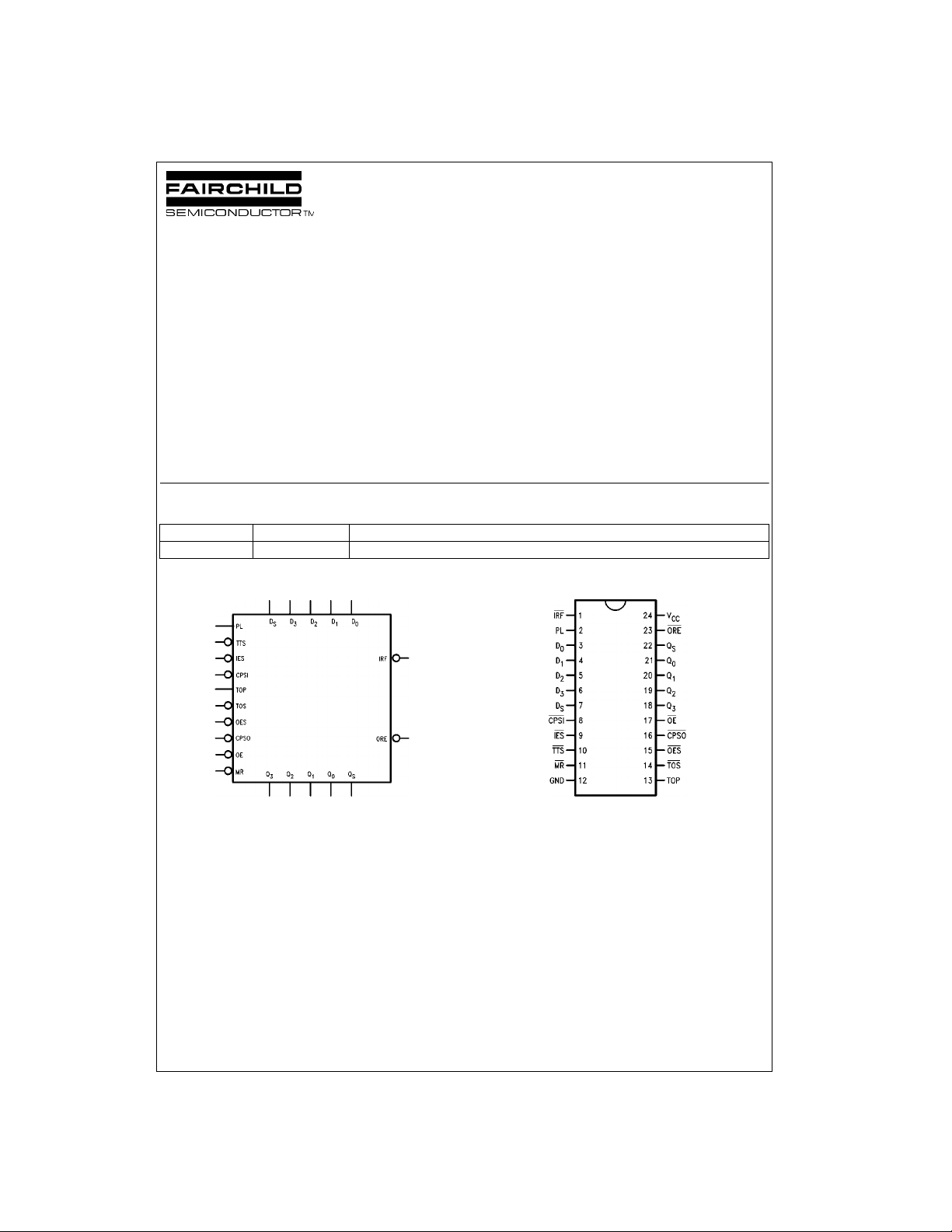
Logic Symbol Connection Diagram
© 1999 Fairchild Semiconductor Corporation DS009544 www.fairchildsemi.com
Page 2
Unit Loading/Fan Out
74F433
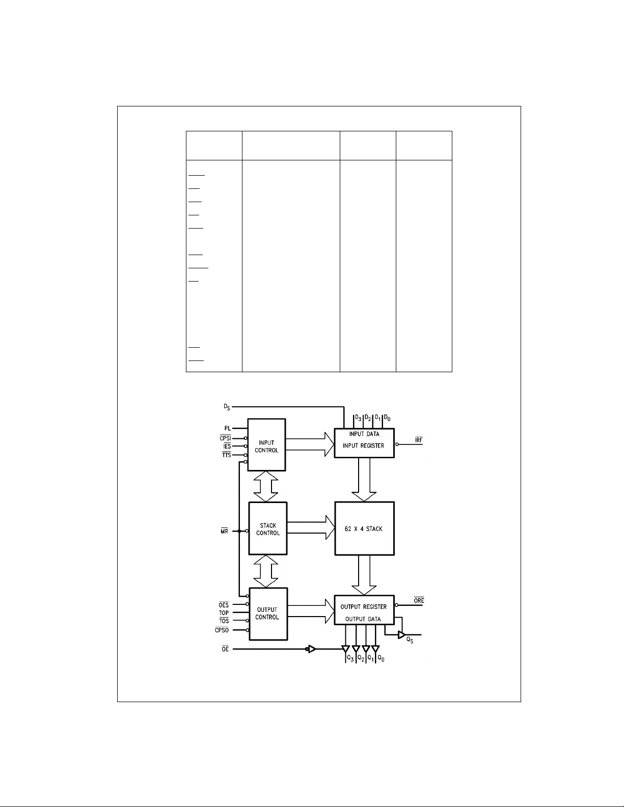
Block Diagram
Pin Names Description
PL Parallel Load Input 1.0/0.66 20 µA/400 µA
CPSI
IES
TTS
MR
OES
TOP Transfer Out Parallel 1.0/0.66 20 µA/400 µA
TOS
CPSO
OE
D
0–D3
D
S
Q
0–Q3
Q
S
IRF
ORE
Serial Input Clock 1.0/0.66 20 µA/400 µA
Serial Input Enable 1.0/0.66 20 µA/400 µA
Transfer to Stack Input 1.0/0.66 20 µA/400 µA
Master Reset 1.0/0.66 20 µA/400 µA
Serial Output Enable 1.0/0.66 20 µA/400 µA
Transfer Out Serial 1.0/0.66 20 µA/400 µA
Serial Output Clock 1.0/0.66 20 µA/400 µA
Output Enable 1.0/0.66 20 µA/400 µA
Parallel Data Inputs 1.0/0.66 20 µA/400 µA
Serial Data Input 1.0/0.66 20 µA/400 µA
Parallel Data Outputs 285/10 5.7 mA/16 mA
Serial Data Output 285/10 5.7 µA/16 mA
Input Register Full 20/5 400 µA/8 mA
Output Register Empty 20/5 400 µA/8 mA
U.L.
HIGH/LOW
Input I
Output I
IH/IIL
OH/IOL
www.fairchildsemi.com 2
Page 3
Functional Description
As shown in the block diagram, the 74F433 co nsists of
three sections:
1. An Input Register with parallel and serial da ta inputs,
as well as control inputs and ou tputs for input handshaking and expansion.
2. A 4-bit-wide, 62-word -deep fall- throug h stack with se lfcontained control logic.
3. An Output Register with parallel and serial data outputs, as well as cont rol inputs and outputs fo r output
handshaking and expansion.
These three sections opera te asynchronously and are virtually independent of one another.
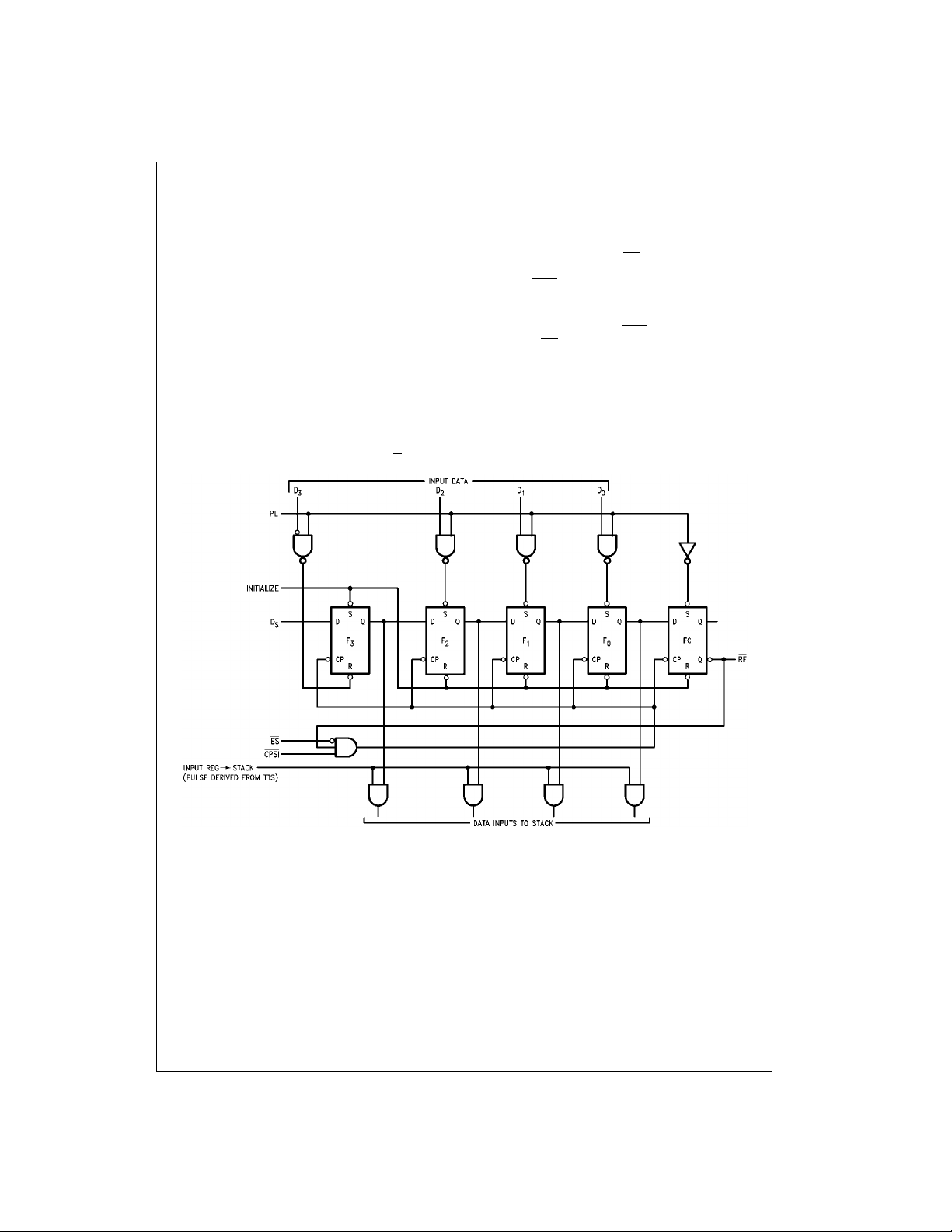
Input Register (Data Entry)
The Input Register can receive data in either bit-serial or 4bit parallel form. It stores t his data u ntil it is sent to the fallthrough stack, and also generates the necessary status
and control signals.
This 5-bit register (see Figure 1) is initialized by setting flip-
and resetting the other flip-flops. The Q-out put of
flop F
3
the last flip-flop (FC) is bro ught out as the Input Register
Full (IRF) signal. After initialization, this output is HIGH.
Parallel Entry—A HIGH on the Parallel Load (PL) input
loads the D
the FC flip-flop. Th i s f orces the IRF
inputs into the F0–F3 flip-flops and sets
0–D3
output LOW, indicating
that the input register is full. During parallel entry, the Serial
Input Clock (CPSI
Serial Entry—Data on the Serial Data (D
entered into the shift registe r (F
HIGH-to-LOW transition of the CPSI
Input Enable (IES
) input must be LOW.
) input is serially
S
, F2, F1, F0, FC) on each
3
input when the Serial
) signal is LOW. During serial e ntry, the
PL input should be LOW.
After the fourth clock transition, the four data bits are
located in flip-flops F
output LOW and intern ally inhibiting CPSI pulses
the IRF
. The FC flip-flop is set, forcing
0–F3
from affecting the register. Figure 2 illustrates the final positions in an 74F43 3 resulting from a 256-bit serial b it train
is the first bit, B
(B
0
the last).
255
74F433
FIGURE 1. Conceptual Input Section
3 www.fairchildsemi.com
Page 4

74F433
FIGURE 2. Final Positions in an 74F433
Resulting from a 256-Bit Serial T rain
Fall-Through Stack—The outputs of flip-flops F
the stack. A LOW level on the Transfer to Stack (TTS
initiates a fall-through action; if the top location of the stack
is empty, data is loaded into the stack and the input register
is re-initialized. (Note that this initialization is delayed until
PL is LOW). Thus, automatic F IFO action is achieved by
connecting the IRF
An RS-type flip-flop (the initialization flip-flop) in the control
section records the f act that data has been transferred to
the stack. This prevents mul tiple entry of the same word
into the stack even though IRF
the initialization flip-flop is not cleared until PL goes LOW.
Once in the stack, data falls through automatically, pausing
only when it is necessary to wait for an empty next location.
In the 74F433, the master reset (MR
the stack control section and does not clear the data.
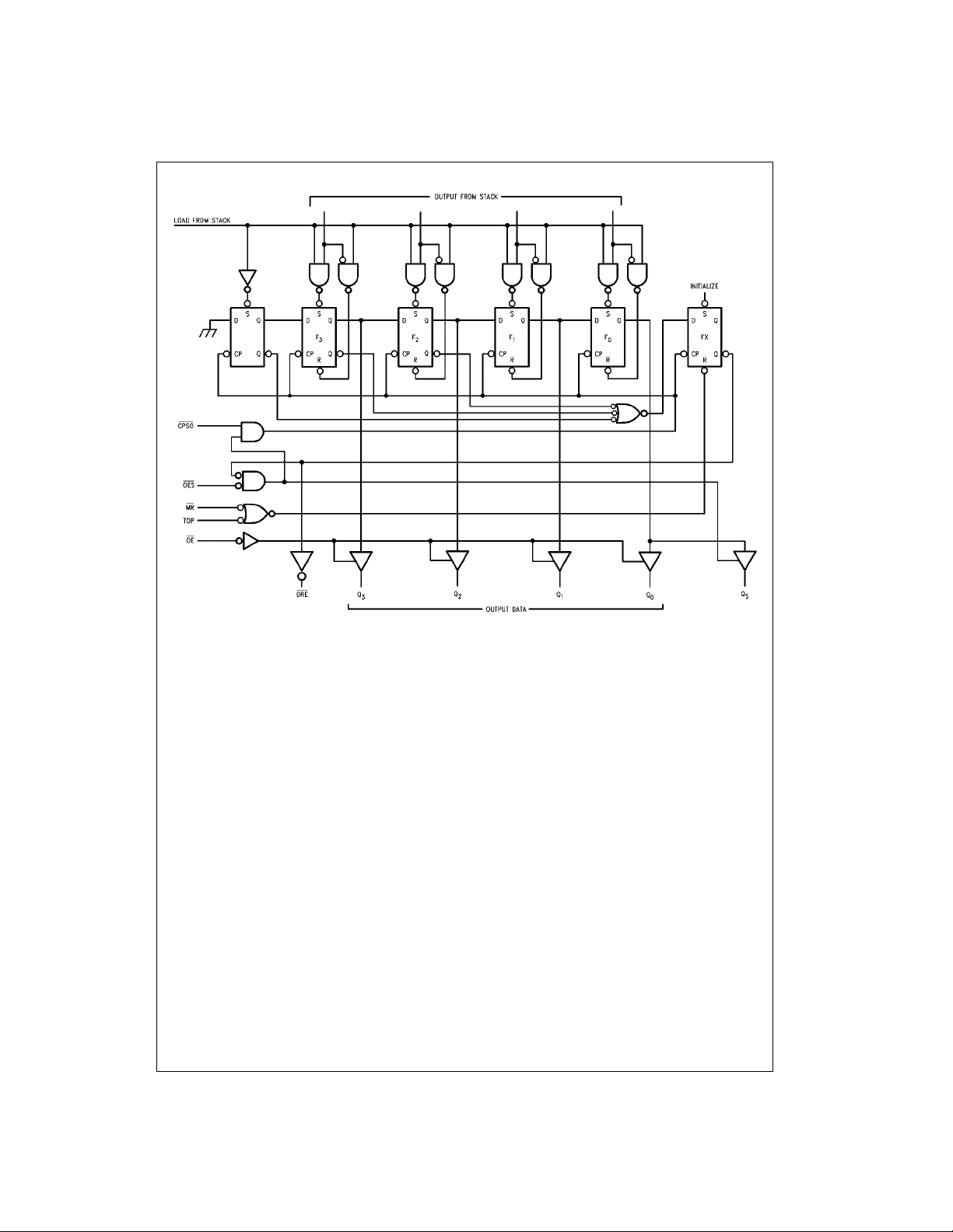
Output Register
The Output Register (see Figure 3) receives 4-bit data
words from the bottom stack location, stores them, and outputs data on a 3-STATE, 4-bit parallel data bus or on a 3 STATE serial data bus. The output secti on generates an d
receives the necessary status and control signals.
Parallel Extraction—W he n the FI FO is e m pt y a ft e r a LO W
pulse is applied to the MR input, the Output Register Empty
) output is LOW. After data has been en ter ed in to th e
(ORE
FIFO and has fallen through to the bottom stack location, it
is transferred into the outp ut register, if the Transfer Out
Parallel (TOP) input is HIGH. A s a r esult of the da ta tran s-
output to the TTS inpu t.
and TTS may still be LOW;
) input only initializes
0–F3
feed
) input
fer, ORE
goes HIGH, indicating valid data on the dat a outputs (provided that the 3-STATE buffer is enabled). The
TOP input can then be used to clock out the next word.
When TOP goes LOW, ORE
that the output data has been extracted; however, the data
itself remains on the output bus until a HIG H level on TOP
permits the transfer of t he next word (if availa ble) into the
output register. During para llel data extraction, the s erial
output clock (CPSO
Serial (TOS
ation or connected to the appropriate ORE
expanded operation (refer to the “Expansion” section).
The TOP signal is not edge-triggered. Therefore , if TOP
goes HIGH before data is available from the stack but data
becomes available before TOP again go es LOW, that data
is transferred into the output register. However, internal
control circuitry prevents the same data from being transferred twice. If TOP goes HIGH and returns to LOW before
data is available f rom the stack, O RE
cating that there is no valid data at the outputs.
Serial Extraction—Wh en the FIFO is empty a fter a LOW
is applied to the MR input, the ORE
data has been entered into the FIFO and has fallen through
to the bottom stack location, it is transferred into the output
register, if the TOS
result of the data transfer, ORE
valid data is in the register.
The 3-STATE Serial Data Output (Q
enabled and puts th e first data bit on the output b us. Data
is serially shifted out on the HIGH-to-LOW transition of
. To prevent false shifting, CPSO should be LOW
CPSO
when the new word is being loaded into the output register.
The fourth transit ion em pties the s hift reg ister, forces O RE
LOW, and disables the serial output, QS. For serial opera-
tion, the ORE
ing a new word from the stack as soon as the previous one
has been shifted out.
Expansion
Vertical Expansion—The 74F433 may be vertically
expanded, without external components, to store more
words. The interconnections necessary to form a 190-word
by 4-bit FIFO are shown in F igure 4. Using th e same te chnique, any FIFO of (63n+1)-wo rds by 4-bits ca n be confi gured, where n is the number of devices. Note that
expansion does not sacrifice any of the 74F433 flexibility
for serial/parallel input and output.
) line should be LO W. The T ra n sf er Ou t
) line should be gr ounde d for s ingle -slice oper-
input is LOW and TOP is HIG H. As a
output may be tied to the TOS input, request-
also goes LOW, indicating
line for
remains LOW, indi-
output is LOW. After
goes HIGH, indicating t hat
) is automatically
S
www.fairchildsemi.com 4
Page 5
74F433
FIGURE 3. Conceptual Output Section
5 www.fairchildsemi.com
Page 6

74F433
FIGURE 4. A Vertical Expansion Scheme
Horizontal Expansion—The 74F433 can be hori zontally
expanded, withou t external logic, to store long words ( in
multiples of 4-bits). The interconnections necessary to form
a 64-word by 12-bit FIFO are shown in Figure 5. Using the
same technique, any FI FO of 64-words by 4n-bits can be
constructed, where n is the number of devices.
The right-most (most significant) device is connected to the
inputs of all devices. Si milarly, the ORE output of th e
TTS
most significant device is con nected to the TOS
all devices. As in the vertical expansion scheme, horizontal
expansion does not sacrifice any of the 74F433 flexibility
for serial/parallel input and output.
www.fairchildsemi.com 6
inputs of
It should be noted that the horizontal expansion scheme
shown in Figure 5 exacts a penalty in speed.
Horizontal and Vertical Expansion—The 74F433 can be
expanded in both the horizontal and vertical directions
without any external components and without sacrificing
any of its FIFO flexibility for serial/parallel input and output.
The interconnections nece ssary to for m a 127-wo rd by 16bit FIFO are shown in Fig ur e 6. Using the same tec hniq ue,
any FIFO of (63m+1)- words by 4n-bits can be configured,
where m is the num ber of de vi ces in a co lu mn an d n is the
number of devices in a row. Figure 7 and Figure 8 illustrate
the timing diagrams f or seria l data ent ry and ext raction for
the FIFO shown in Figure 6. Figure 9 illustrates the final
Page 7

positions of bits in an expanded 74F433 FIFO resulting
from a 2032-bit serial bit train.
Interlocking Circuitry—Most conventi onal FIFO designs
provide status signal analogous to IRF
when these devices are op erated in arrays, variations in
unit-to-unit operating speed require external gating to
ensure that all devices ha ve completed an oper ation. The
74F433 incorporates simple but effective 'master/slave'
interlocking circuitry to eliminat e the nee d for exte rnal gating.
In the 74F433 arra y of Figure 6, devices 1 and 5 are the
row masters; the other devices are slave s to the master in
their rows. No slave in a given row initializes its input register until it has receiv ed a LOW on its IES
master or a slave of higher priority.
Similarly, the ORE
their inputs have gone HIGH. This interlocking scheme
ensures that new input da ta may b e accept ed by the arr ay
when the IRF
HIGH and that output data for the arr ay may be extracted
when the ORE
goes HIGH.
outputs of slaves do not go HIGH until
output of the final slave in that row goes
output of the final slav e in the output row
and ORE. However,
input from a row
The row master is estab lished by connecting its IES
to ground, while a slave receives its IES
output of the next-higher pri ority device. When an array of
74F433 FIFOs is initialized with a HIGH on the MR in puts
of all devices, the IRF
Thus, only the row master receives a LOW on the IES
during initialization.
Figure 10 is a conceptua l logic diagram of the internal ci rcuitry that determines ma ster/slave operation. When MR
and IES are LOW, the master latch is set. When TTS goes
LOW, the initialization flip-flop is set. If the master latch is
HIGH, the input register is immediately initialized and the
initialization flip-flop reset. If the master latch is re set, the
input register is not initialized until IES
operation, activating TTS
tialization from the row master to the last slave.
A similar operation takes place for the output register.
Either a TOS
ation and sets the ORE
is set, the last output regi ster flip-flop is set and the ORE
line goes HIGH. If the master latch is reset, the ORE output
is LOW until a Serial Output Enable (OES
received.
or TOP input initiates a load-from-stack oper-
outputs of all devices are HIGH.
initiates a ripple input register ini-
request flip-flop. If the m aste r latch
input from the IRF
goes LOW. In array
input
input
) input is
74F433
FIGURE 5. A Horizontal Expansion Scheme
7 www.fairchildsemi.com
Page 8

74F433
FIGURE 6. A 127 x 16 FIFO Array
FIGURE 7. Serial Data Entry for Array of Figure
www.fairchildsemi.com 8
Page 9

74F433
FIGURE 8. Serial Data Extraction for Array of Figure
FIGURE 9. Final Position of a 2032-Bit Serial Input
FIGURE 10. Conceptual Diagram, Interlocking Circuitry
9 www.fairchildsemi.com
Page 10

Absolute Maximum Ratings(Note 1) Recommended Operating
Storage Temperature −65°C to +150°C
74F433
Ambient Temperature under Bias −55°C to +125°C
Junction Temperature under Bias −55°C to +150°C
Pin Potential to
V
CC
Ground Pin −0.5V to +7.0V
Input Voltage (Note 2) −0.5V to +7.0V
Input Current (Note 2) −30 mA to +5.0 mA
Voltage Applied to Output
in HIGH State (with V
CC
= 0V)
Standard Output −0.5V to V
3-STATE Output −0.5V to +5.5V
Current Applied to Output
in LOW State (Max) twice the rated I
OL
Conditions
Free Air Ambient Temperature 0°C to +70°C
Supply Voltage +4.5V to +5.5V
Note 1: Absolute maximum ratings are values beyond which the device
may be damaged or have its useful life impaired. Functional operation
CC
under these conditi ons is not implied.
Note 2: Either voltage limit or curren t limit is sufficient to protect in put s .
(mA)
DC Electrical Characteristics
Symbol Parameter Min Typ Max Units
V
V
V
V
V
I
IH
I
BVI
I
CEX
V
I
OD
I
IL
I
OZH
I
OZL
I
OS
I
CC
IH
IL
CD
OH
OL
ID
Input HIGH Voltage 2.0 V Recognized as a HIGH Signal
Input LOW Voltage 0.8 V Recognized as a LOW Signal
Input Clamp Diode Voltage −1.5 V Min IIN = −18 mA
Output HIGH 10% V
Voltage 10% V
5% V
5% V
Output LOW Voltage 10% V
Input HIGH Current 5.0 µAMaxVIN = 2.7V
Input HIGH Current
Breakdown Test
Output HIGH
Leakage Current
Input Leakage
Test All Other Pins Grounded
Output Leakage
Circuit Current All Other Pins Grounded
Input LOW Current −0.4 mA Max VIN = 0.5V
Output Leakage Current 50 µAMaxV
Output Leakage Current −50 µAMaxV
Output Short-Circuit Current −20 −130 mA Max V
Power Supply Current 150 215 mA Max
2.4
CC
2.4 IOH = 5.7 mA (Qn, Qs)
CC
2.7 IOH = 400 µA (ORE, IRF)
CC
2.7 IOH = 5.7 mA (Qn, Qs)
CC
CC
4.75 V 0.0
0.50 V Min IOL = 16 mA (Qn, Qs)
7.0 µAMax
50 µAMax
3.75 µA0.0
V
CC
IOH = 400 µA (ORE, IRF)
VMin
VIN = 7.0V
V
IID = 1.9 µA
V
Conditions
= V
OUT
CC
= 150 mV
IOD
= 2.7V (Qn, Qs)
OUT
= 0.5V (Qn, Qs)
OUT
= 0V
OUT
www.fairchildsemi.com 10
Page 11

AC Electrical Characteristics
Symbol Parameter
t
t
t
t
t
t
t
t
t
t
t
t
t
t
t
t
t
t
t
t
t
t
t
t
t
t
t
t
t
PHL
PLH
PLH
PHL
PLH
PHL
PHL
PHL
PLH
PLH
PHL
PLH
PLH
PLH
PHL
PLH
PZH
PZL
PHZ
PLZ
PZH
PZL
PHZ
PLZ
PZH
PZL
DFT
AP
AS
Propagation Delay, Negative-Going
CPSI to IRF Output
Propagation Delay,
Negative-Going TTS to IRF
Propagation Delay, Negative-Going 4.0 25.0 3.0 27.0
CPSO to QS Output 5.0 20.0 5.0 21.0
Propagation Delay, Positive-Going 8.0 35.0 7.0 38.0
TOP to Q0–Q3 Outputs 7.0 30.0 7.0 32.0
Propagation Delay,
Negative-Going CPSO to ORE
Propagation Delay,
Negative-Going TOP to ORE
Propagation Delay, Positive-Going
TOP to ORE
Propagation Delay, Negative-Going
TOS to Positive-Going ORE
Propagation Delay, PositiveGoing PL to Negative-Going IRF
Propagation Delay, NegativeGoing PL to Positive-Going IRF
Propagation Delay,
Positive-Going OES to ORE
Propagation Delay Positive-IRF
Going IES to Positive-Going
Propagation Delay
MR to ORE
Propagation Delay
MR to IRF
Enable Time 1.0 16.0 1.0 18.0
OE to Q0–Q
3
Disable Time 1.0 10.0 1.0 12.0
OE to Q0–Q
3
Enable Time 1.0 10.0 1.0 12.0
Negative-Going OES to Q
S
Disable Time 1.0 10.0 1.0 12.0
Negative-Going OES to Q
S
Enable Time 1.0 35.0 1.0 42.0
TOS to Q
S
Fall-Through Time 0.2 0.9 0.2 1.0 ns Figure 16
Parallel Appearance Time
ORE to Q0–Q
3
Serial Appearance Time
ORE to Q
S
TA = +25°CT
VCC = +5.0V VCC = +5.0V
CL = 50 pF CL = 50 pF
= 0°C to +70°C
A
Units
Figure
Number
Min M ax Min Max
2.0 17.0 2.0 18.0
9.0 34.0 8.0 38.0
Figure 11
ns
Figure 12
Figure 13
ns
Figure 14
ns Figure 15
7.0 25.0 6.0 28.0 ns
Figure 13
Figure 14
6.0 26.0 6.0 28.0
ns Figure 15
13.0 48.0 12.0 51.0
13.0 45.0 12.0 50.0 ns
4.0 22.0 4.0 23.0
7.0 31.0 6.0 35.0
Figure 13
Figure 14
Figure 17
ns
Figure 18
9.0 38.0 8.0 44.0 ns
5.0 25.0 5.0 27.0 ns Figure 18
7.0 28.0 7.0 31.0 ns
5.0 27.0 5.0 30.0 ns
1.0 14.0 1.0 16.0
ns
1.0 23.0 1.0 30.0
1.0 14.0 1.0 15.0
ns
1.0 14.0 1.0 16.0
1.0 35.0 1.0 39.0
ns
−20.0 −2.0 −20.0 −2.0
ns
−20.0 5.0 −20.0 5.0
74F433
11 www.fairchildsemi.com
Page 12

AC Operating Requirements
74F433
Symbol Parameter
tS(H) Setup Time, HIGH or LOW 7.0 7.0
tS(L) DS to Negative CPSI 7.0 7.0
tH(H) Hold Time, HIGH or LOW 2.0 2.0
tH(L) DS to CPSI 2.0 2.0
tS(L) Setup Time, LOW TTS to IRF,
tS(L) Setup Time, LOW Negative-Going
tS(L) Setup Time, LOW Negative-Going
tS(L) Setup Time, LOW Negative-Going
tS(H) Setup Time, HIGH or LOW 0.0 0.0 ns
tS(L) Parallel Inputs to PL 0.0 0.0
tH(H) Hold Time, HIGH or LOW 4.0 4.0
tH(L) Parallel Inputs to PL 4.0 4.0
tW(H) CPSI Pulse Width 10.0 11.0
tW(L) HIGH or LOW 5.0 6.0
tW(H) PL Pulse Width, HIGH 7.0 9.0 ns Figure 17
tW(L)
tW(L) MR Pulse Width, LOW 7.0 9.0 ns Figure 16
tW(H) TOP Pulse Width 14.0 16.0
tW(L) HIGH or LOW 7.0 7.0
tW(H) CPSO Pulse Width 14.0 16.0
tW(L) HIGH or LOW 7.0 7.0
t
REC
Serial or Parallel Mode
ORE to Negative-Going TOS
IES to CPSI
TTS to CPSI
TTS Pulse Width, LOW
Serial or Parallel Mode
Recovery Time
MR to Any Input
TA = +25°CT
VCC = +5.0V
Min Max Min Max
0.0 0.0 ns
0.0 0.0 ns
8.0 9.0
30.0 33.0
7.0 9.0 ns
8.0 15.0 ns Figure 16
= 0°C to +70°C
A
VCC = +5.0V
Units
ns
ns Figure 12
ns
ns Figure 15
ns
Figure
Number
Figure 11
Figure 12
Figure 11
Figure 12
Figure 17
Figure 18
Figure 13
Figure 14
Figure 11
Figure 12
Figure 18
Figure 11
Figure 12
Figure 13
Figure 14
Figure 13
Figure 14
www.fairchildsemi.com 12
Page 13

Timing Waveforms
74F433
Conditions: Stack not f ull, I ES, PL LOW
Conditions: Stack not f ull, I ES HIGH when initiated, PL LOW
FIGURE 11. Serial Input, Unexpanded or Master Operation
FIGURE 12. Serial Input, Expanded Slave Operation
Conditions: Data in stack, TOP HIGH, IES LOW when initiated, OES LOW
FIGURE 13. Serial Output, Unexpanded or Master Operation
13 www.fairchildsemi.com
Page 14

Timing Waveforms (Continued)
74F433
Conditions: Data in stack, TOP HIGH, IES HIGH when initiated
Conditions: IES LOW when initiated, O E, CPSO L OW ; da t a av ailable in stack
FIGURE 15. Parallel Output, 4-Bit Word or Master in Parallel Expansion
Conditions: TTS connected to IRF, TOS connected to ORE, IES, OES, OE, CPSO LOW, TOP HIGH
FIGURE 14. Serial Output, Slave Operation
FIGURE 16. Fall Through Time
www.fairchildsemi.com 14
Page 15

Timing Waveforms (Continued)
Conditions: Stack not f ull, I ES LOW when initialized
NOTE A: TTS normally connected to IRF.
NOTE B: If stack is full, IRF
FIGURE 17. Parallel Load Mode, 4-Bit Word (Unexpanded) or Master in Parallel Expansion
will stay LOW.
74F433
Conditions: Stack not f ull, device initialized (No te 3) w it h I ES HIGH
Note 3: Initialization requires a master reset to oc c ur after power has been applied.
FIGURE 18. Parallel Load, Slave Mode
15 www.fairchildsemi.com
Page 16

Physical Dimensions inches (millimeters) unless otherwise noted
74F433 First-In First-Out (FIFO) Buffer Memory
Fairchild does not assume any responsibility for us e of any circuitry described, no circuit patent licenses are implied and
Fairchild reserves the right at any time without notice to change said circuitry and specifications.
LIFE SUPPORT POLICY
FAIRCHILD’S PRODUCTS ARE NOT AUTHORIZED FOR USE AS CRITICAL COMPONENTS IN LIFE SUPPORT
DEVICES OR SYSTEMS WITHOUT THE EXPRESS WRITTEN APPROVAL OF THE PRESIDENT OF FAIRCHILD
SEMICONDUCTOR CORPORATION. As used herein:
1. Life support devices or systems are devices or syste ms
which, (a) are intended for surgical implant into the
body, or (b) support or sustain life, and (c) whose failure
to perform when properly used in accordance with
instructions for use provided in the labeling, can be reasonably expected to result in a significan t injury to the
user.
24-Lead Plastic Dual-In-Line Package (PDIP), JEDEC MS-100, 0.300 Wide
Package Number N24C
2. A critical component in any compon ent of a lif e supp ort
device or system whose failu re to perform can be reasonably expected to ca use the fa i lure of the li fe su pp ort
device or system, or to affect its safety or effectiveness.
www.fairchildsemi.com
www.fairchildsemi.com 16
 Loading...