

Page 1
April 1988
Revised August 1999
74F413
64 x 4 First-In First-Out Buffer Memory with Parallel I/O
74F413 64 x 4 First-In First-Out Buffer Memory with Parallel I/O
General Description
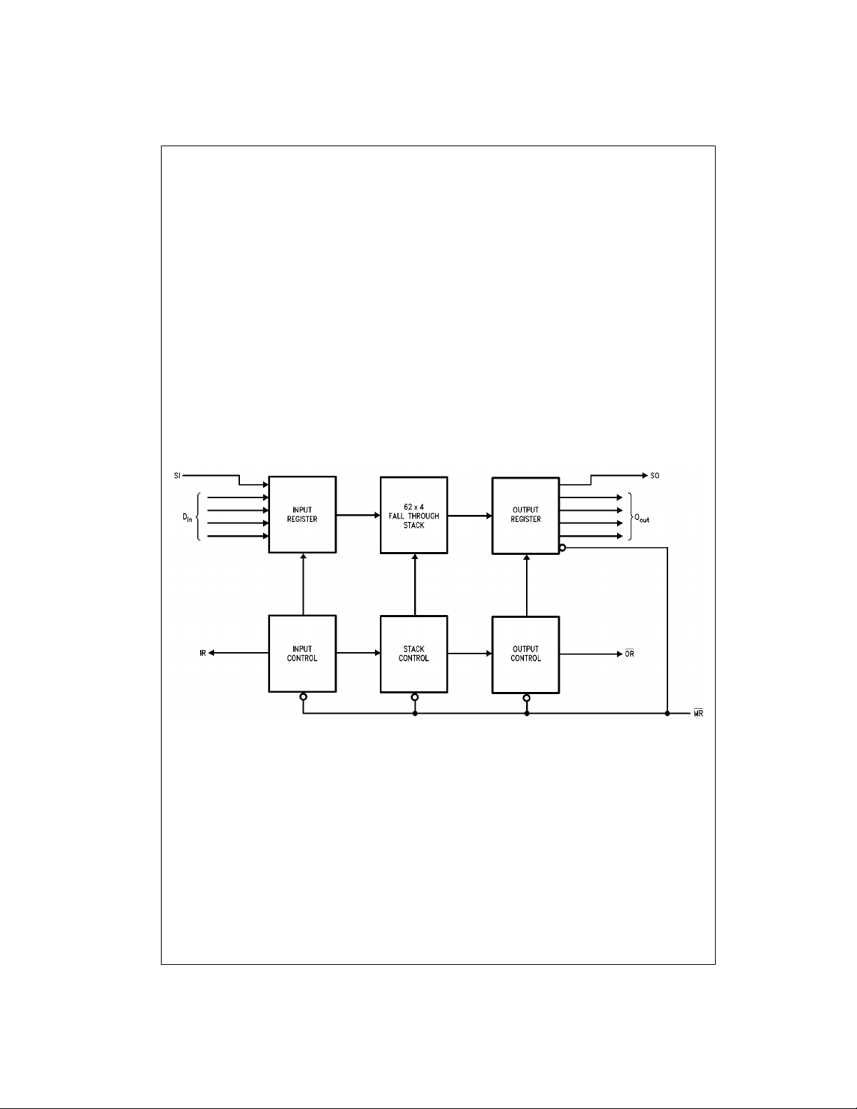
The F413 is an expandabl e fall-through type high-speed
First-In First-Out (FIFO) buffer memory organized as 64
words by four bits. The 4-bit input and output registers
record and transmit, respectively, asynchronous data in
parallel form. Control pins on the input and ou tput al low f or
handshaking and expa nsion. The 4-bit wide, 62-bit deep
fall-through stack has self-contained control logic.
Features
■ Separate input and output clocks
■ Parallel input and output
■ Expandable without external logic
■ 15 MHz data rate
■ Supply current 160 mA max
■ Available in SOIC, (300 mil only)
Ordering Code:
Order Number Package Number Package Description
74F413PC N16E 16-Lead Plastic Dual-In-Line Package (PDIP), JEDEC MS-001, 0.300 Wide
Devices also availab le in Tape and Reel. Specify by appending th e s uffix let t er “X” to the ordering cod e.
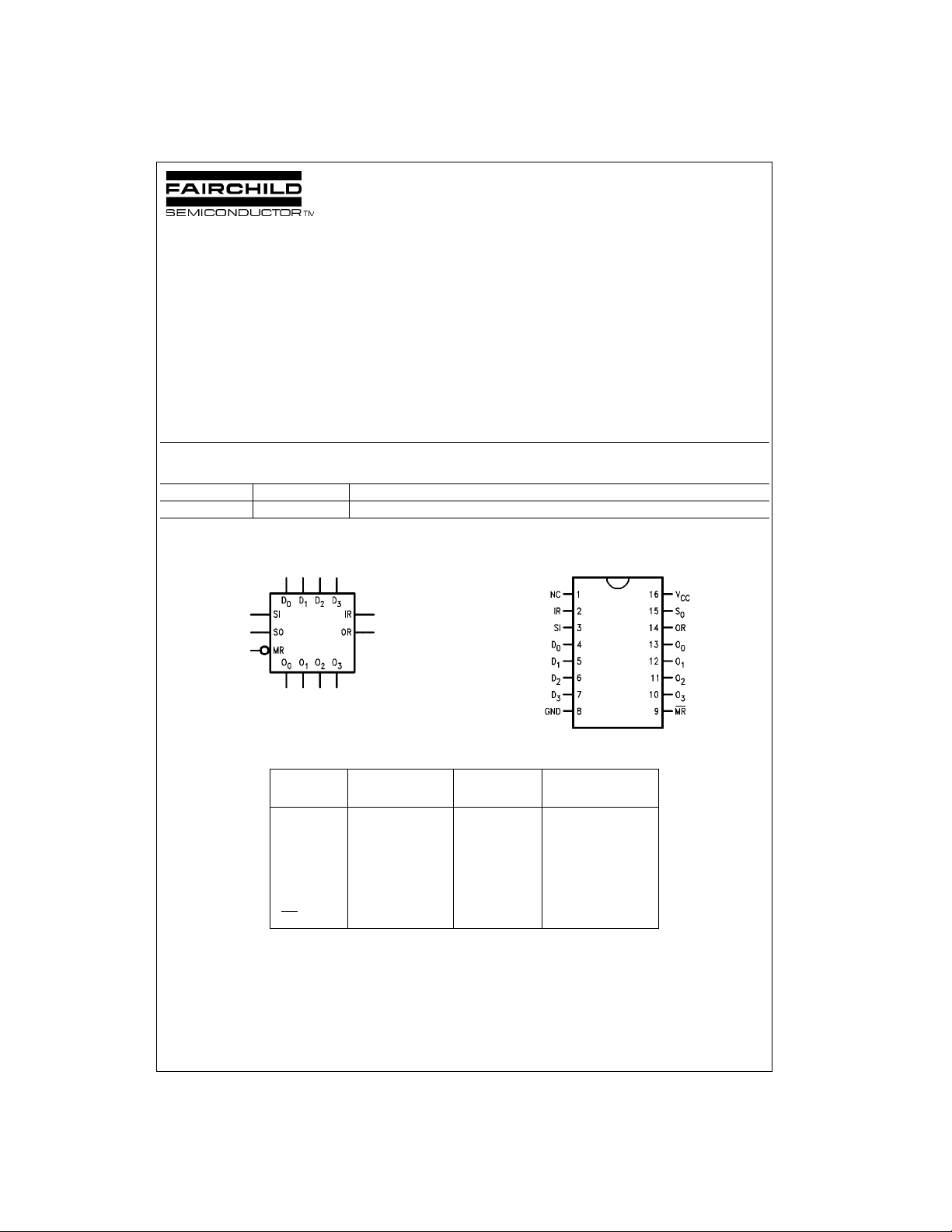
Logic Symbol Connection Diagram
Unit Loading/Fan Out
Pin Names Description
D0–D
O
0–O3
IR Input Ready 1.0/0.667 20 µA/−0.4 mA
SI Shift In 1.0/0.667 20 µA/−0.4 mA
SO Shift Out 1.0/0.667 20 µA/−0.4 mA
OR Output Ready 1.0/0.667 20 µA/−0.4 mA
MR
Data Inputs 1.0/0.667 20 µA/−0.4 mA
3
Data Outputs 50/13.3 −1 mA/8 mA
Master Reset 1.0/0.667 20 µA/−0.4 mA
U.L.
HIGH/LOW
Input I
Output I
IH/IIL
OH/IOL
© 1999 Fairchild Semiconductor Corporation DS009541 www.fairchildsemi.com
Page 2
Functional Description
Data Input— Data is entered into the FIFO on D0–D
inputs. To enter data the Input Ready (IR) should be HIGH,
74F413
indicating that the first location is ready to accept data.
Data then present at the four data inputs is entered into the
first location when the Shift In (SI) is broug ht HIGH. An SI
HIGH signal causes the IR to go LOW. Data remains at the
first location unti l SI is brought LOW. When SI is brought
LOW and the FIFO is not full, I R will go HIGH, indicating
that more room is available. Simultaneously, data will propagate to the second location and continue shifting until it
reaches the output stage or a full location. If the memory is
full, IR will remain LOW.
Data Transfer— Once data is entered into the second cell,
the transfer of any full cell to the adjacen t (downstream)
empty cell is automatic, activated by an on-chip control.
Thus data will stack up at the end of the device while empty
locations will “bubble” to the front. The t
parameter
PT
Block Diagram
defines the time requir ed for the first data to travel from
3
input to the output of a previously empty device.
Data Output— Data is read from the O
When data is shifted to the output stage, Output Ready
(OR) goes HIGH, indicating the presence of valid data.
When the OR is HIGH, data may be shifted out by bringing
the Shift Out (SO) HIGH. A HIGH signal at SO causes the
OR to go LOW. Valid data is maintained while the SO is
HIGH. When SO is brought LOW, the upstream da ta, provided that stage has valid data, is shifted to the output
stage. When new val id data is shif ted to the ou tput stage,
OR goes HIGH. If the FIFO is emptied, OR stays LOW, and
remains as before, i.e., data does not change if
O
0–O3
FIFO is empty.
Input Ready and Outpu t Ready— may also be used as
status signals indicating that the FIFO is completely full
(Input Ready stays LOW for at least t
empty (Output Ready stays LOW for at least t
0–O3
) or completely
PT
).
PT
outputs.
www.fairchildsemi.com 2
Page 3

Absolute Maximum Ratings(Note 1) Recommended Operating
Storage Temperature −65°C to +150°C
Ambient Temperature under Bias −55°C to +125°C
Junction Temperature under Bias −55°C to +150°C
Pin Potential to Ground Pin −0.5 V to +7.0V
V
CC
Input Voltage (Note 2) −0.5V to +7.0V
Input Current (Note 2) −30 mA to +5.0 mA
Voltage Applied to Output
in HIGH State (with V
CC
= 0V)
Standard Output −0.5V to V
3-STATE Output −0.5V to +5.5V
Current Applied to Output
in LOW State (Max) twice the rated I
OL
Conditions
Free Air Ambient Temperature 0°C to +70°C
Supply Voltage +4.5V to +5.5V
Note 1: Absolute maximum ratings are values beyon d which the device
may be damaged or have its useful life impaired . Functional operation
CC
under these condit ions is not implied.
Note 2: Either voltage limit or curren t limit is sufficient to protect in puts.
(mA)
DC Electrical Characteristics
74F413
Symbol Parameter Min Typ Max Units
V
V
V
V
V
I
I
I
V
I
I
I
I
IH
IL
CD
OH
OL
IH
BVI
CEX
ID
OD
IL
OS
CCH
Input HIGH Voltage 2.0 V Recognized as a HIGH Signal
Input LOW Voltage 0.8 V Recognized as a LOW Signal
Input Clamp Diode Voltage −1.5 V Min IIN = −18 mA
Output HIGH 10% V
Voltage 5% V
Output LOW Voltage 10% V
Input HIGH Current 5.0 µAMaxVIN = 2.7V
Input HIGH Current
Breakdown Test
Output HIGH Leakage Current 50 µAMaxV
Input Leakage
Test All Other Pins Grounded
Output Leakage
Circuit Current All Other Pins Grounded
Input LOW Current −0.4 mA Max VIN = 0.5V
Output Short-Circuit Current −20 −130 mA Max V
Power Supply Current 115 160 mA Max VO = HIGH
CC
CC
CC
2.4
2.7 IOH = −1 mA
0.5 V Min IOL = 8 mA
7.0 µAMaxVIN = 7.0V
4.75 V 0.0
3.75 µA0.0
V
CC
VMin
IOH = −1 mA
IID = 1.9 µA
V
= V
OUT
= 150 mV
IOD
= 0V
OUT
Conditions
CC
3 www.fairchildsemi.com
Page 4

AC Electrical Characteristics
74F413
Symbol Parameter
f
f
t
t
t
t
t
t
t
t
MAX
MAX
PLH
PHL
PLH
PHL
PLH
PHL
PLH
PLH
Shift In Rate 10 8.0 10 MHz
Shift Out Rate 10 8.0 10 MHz
Propagation Delay 1.5 44.0 1.5 50.0 1.5 48.0
Shift In to IR 1.5 31.0 1.5 37.0 1.5 35.0
Propagation Delay 1.5 52.0 1.5 57.0 1.5 55.0
Shift Out to OR 1.5 31.0 1.5 37.0 1.5 35.0
Propagation Delay 1.5 46.0 1.5 52.0 1.5 50.0
Output Data Delay 1.5 34.0 1.5 39.0 1.5 37.0
Propagation Delay 1.5 27.0 1.5 33.0 1.5 31.0 ns
Master Reset to IR
Propagation Delay 1.5 30.0 1.5 34.0 1.5 32.0 ns
Master Reset to OR
TA = +25°CT
VCC = +5.0V VCC = +5.0V VCC = +5.0V
CL = 50 pF CL = 50 pF CL = 50 pF
Min Typ Max Min Max Min Max
= −55°C to +125°CTA = 0° to +70°C
A
AC Operating Requirements
TA = +25°CTA = −55°C to +125°CTA = 0° to +70°C
Symbol Parameter
tS(H) Setup Time, HIGH or LOW 1.0 1.0 1.0 ns
tS(L) Dn to SI 1.0 1.0 1.0
tH(H) Hold Time, HIGH or LOW 10.0 10.0 10.0
tH(L) Dn to SI 10.0 10.0 10.0
tW(H) Shift In Pulse Width 5.0 5.0 5.0 ns
tW(L) HIGH or LOW 10.0 10.0 10.0
tW(H) Shift Out Pulse Width 7.5 8.5 7.5
tW(L) HIGH or LOW 10.0 10.0 10.0
tW(H) Input Ready Pulse Width, 7.5 8.5 7.5 ns
tW(L) Output Ready Pulse Width, 5.0 5.0 5.0 ns
tW(L) Master Reset Pulse Width, 10.0 10.0 10.0 ns
t
REC
t
PT
HIGH
LOW
LOW
Recovery Time, MR to SI 32.0 35.0 35.0 ns
Data Throughput Time 0.9 1.0 1.0 µs
Min Max Min Max Min Max
Units
ns
ns
ns
UnitsVCC = +5.0V VCC = +5.0V VCC = +5.0V
www.fairchildsemi.com 4
Page 5

Physical Dimensions inches (millimeters) unless otherwise noted
74F413 64 x 4 First-In First-Out Buffer Memory with Parallel I/O
16-Lead Plastic Dual-In-Line Package (PDIP), JEDEC MS-001, 0.300 Wide
Fairchild does not assume any responsibility for use of any circuitry described, no circuit patent license s are implied and
Fairchild reserves the right at any time without notice to change said circuitry and specifications.
LIFE SUPPORT POLICY
FAIRCHILD’S PRODUCTS ARE NOT AUTHORIZED FOR USE AS CRITICAL COMPONENTS IN LIFE SUPPORT
DEVICES OR SYSTEMS WITHOUT THE EXPRESS WRITTEN APPROVAL OF THE PRESIDENT OF FAIRCHILD
SEMICONDUCTOR CORPORATION. As used herein:
1. Life support devices or systems are devices or systems
which, (a) are intended for surgical implant into the
body, or (b) support or sustain life, and (c) whose failure
to perform when properly used in accordance with
instructions for use provide d in the labe l ing, can be re asonably expected to result in a significant injury to the
user.
Package Number N16E
2. A critical componen t in any com ponen t of a life s upport
device or system whose failu re to perform can b e reasonably expected to cause the failure of the life support
device or system, or to affect its safety or effectiveness.
www.fairchildsemi.com
5 www.fairchildsemi.com
 Loading...