

Page 1
© 1999 Fairchild Semiconductor Corporation DS009529 www.fairchildsemi.com
May 1988
Revised August 1999
74F382 4-Bit Arithmetic Logic Unit
74F382
4-Bit Arithmetic Logic Unit
General Description
The 74F382 p er f or ms t h re e ar it h me ti c an d th r ee lo gic operations on two 4-bit w ords, A and B. Two additional S elect
input codes force the F unction outputs LOW or HIGH. An
Overflow output is p rovided for conven ience in twos com plement arithmetic. A Carry output is provided for ripple
expansion. For high-speed expansion using a Carry Lookahead Generator, refer to the 74F381 data sheet.
Features
■ Performs six arithmetic and logic functions
■ Selectable LOW (clear) and HIGH (preset) functions
■ LOW input loading minimizes drive requirements
■ Carry output for ripple expansion
■ Overflow output for twos complement arithmetic
Ordering Code:
Devices also availab le in Tape and Reel. Specify by appending th e s uffix let t er “X” to the ordering code.
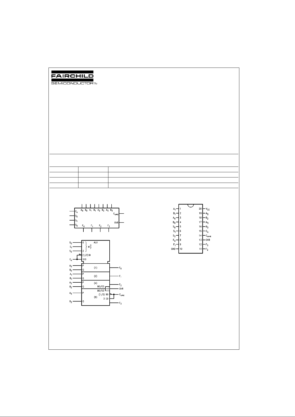
Logic Symbols
IEEE/IEC
Connection Diagram
Order Number Package Number Package Description
74F382SC M20B 20-Lead Small Outline Integrated Circuit (SOIC), JEDEC MS-013, 0.300 Wide
74F382SJ M20D 20-Lead Small Outline Package (SOP), EIAJ TYPE II, 5.3mm Wide
74F382PC N20A 20-Lead Plastic Dual-In-Line Package (PDIP), JEDEC MS-001, 0.300 Wide
Page 2
www.fairchildsemi.com 2
74F382
Unit Loading/Fan Out
Functional Description
Signals applied to the Select inputs S0–S2 determine the
mode of operation, as indicated in the Function Select
Table. An extensive listing of input and output levels is
shown in the Truth Table. The circuit perform s the arithmetic functions for eit her active HIGH or active LOW o perands, with output levels in the same convention. In the
Subtract operating m odes, it is necessa ry to force a carry
(HIGH for active HIGH operands, LOW for active LOW
operands) into the C
n
input of the least significant package.
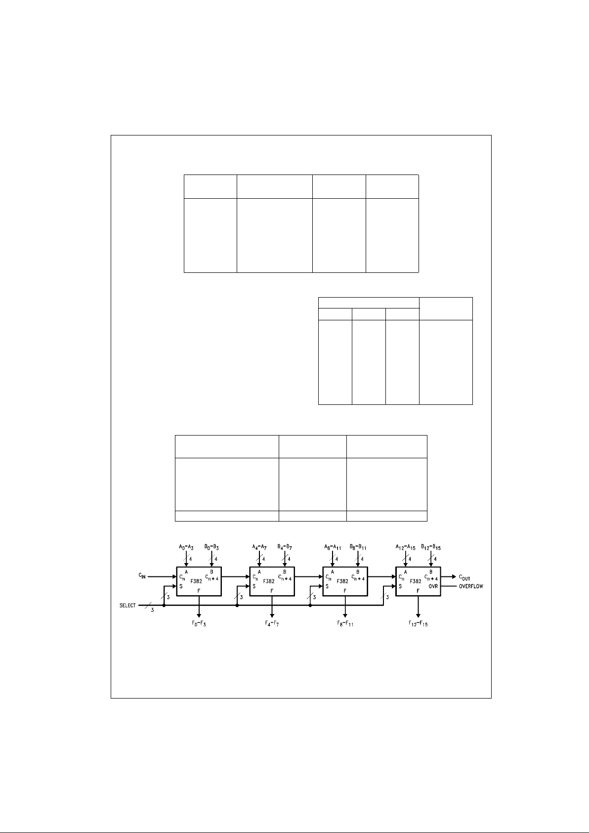
Ripple expansion is illustrated in Figure 2. The overflow
output OVR is the Exclusive-OR of C
n + 3
and C
n + 4
; a
HIGH signal on OVR indica tes overflow in twos complement operation. Typical delays fo r Figure 2 are given in
Figure 1.
Function Select Table
H = HIGH Voltage Level
L = LOW Voltage Level
FIGURE 1. 16-Bit Delay Tabulation
FIGURE 2. 16-Bit Ripply Carry ALU Expansion
Pin Names Description
U.L.
Input I
IH/IIL
HIGH/LOW
Output I
OH/IOL
A0–A
3
A Operand Inputs 1.0/4.0 20 µA/−2.4 mA
B
0–B3
B Operand Inputs 1.0/4.0 20 µA/−2.4 mA
S
0–S2
Function Select Inputs 1.0/1.0 20 µA/−0.6 mA
C
n
Carry Input 1.0/5.0 20 µA/−3.0 mA
C
n + 4
Carry Output 50/33.3 −1 mA/20 mA
OVR Overflow Output 50/33.3 −1 mA/20 mA
F
0–F3
Function Outputs 50/33.3 −1 mA/20 mA
Select
Operation
S
0
S
1
S
2
L L L Clear
H L L B Minus A
L H L A Minus B
HHLA Plus B
LLHA ⊕ B
HLHA + B
LHHAB
HHHPreset
Path Segment
Toward Output
F
C
n + 4
, OVR
A
1
or B1 to C
n + 4
6.5 ns 6.5 ns
C
n
to C
n + 4
6.3 ns 6.3 ns
C
n
to C
n + 4
6.3 ns 6.3 ns
C
n
to F 8.1 ns —
C
n
to C
n + 4
, OVR — 8.0 ns
Total Delay 27.2 ns 27.1 ns
Page 3
3 www.fairchildsemi.com
74F382
Truth Table
H = HIGH Voltage Level L = LOW Voltage Level X = Immaterial
Inputs Outputs
Function
S
0
S
1
S
2
C
n
A
n
B
n
F
0
F
1
F
2
F
3
OVR
C
n + 4
CLEAR LLLLXXLLLLH H
HXXLLLLH H
B MINUS AHLLLLLHHHHL L
LLHLHHHL H
LHLLLLL L L
LHHHHHH L L
HLLLLLLL H
HLHHHHH L H
HHLHLL L L L
HHHL LL L L H
A MINUS B L H L L L L H H H H L L
LLHLLLL L L
LHLLHHH L H
LHHHHHH L L
HLLLLLLL H
HLHHLLL L L
HHLHHHH L H
HHHL LL L L H
A PLUS B HHLLLLLLLLL L
LLHHHHH L L
LHLHHHH L L
LHHLH H HL H
HLLHLLL L L
HLHLLLLL H
HHLLLLLL H
HHHHHHH L H
A ⊕ B LLHXLLLLLLL L
XLHHHHH L L
LHLHHHH L L
XHHLLLLH H
HHLHHHH H H
A + B HLHXLLLLLL L L
XLHHHHH L L
XHLHHHH L L
LHHHHHH L L
HHHHHHHH H
AB LHHXLLLLLLH H
XLHLLLLL L
XHLLLLLH H
LHHHHHH L L
HHHHHHHH H
PRESET H H H X L L H H H H L L
XLHHHHH L L
XHLHHHH L L
LHHHHHH L L
HHHHHHHH H
Page 4

www.fairchildsemi.com 4
74F382
Logic Diagram
Please note that this diagram is provided o nly f or t he understanding of lo gic operations and should not be used to estimate propagation delays.
Page 5

5 www.fairchildsemi.com
74F382
Absolute Maximum Ratings(Note 1) Recommended Operating
Conditions
Note 1: Absolute maximum ratings are values beyon d which the device
may be damaged or have its useful life impaired . Functional operation
under these condit ions is not implied.
Note 2: Either voltage limit or curren t limit is sufficient to protect in puts.
DC Electrical Characteristics over Operating Temperature Range unless otherwise specified
Storage Temperature −65°C to +150°C
Ambient Temperature under Bias −55°C to +125°C
Junction Temperature under Bias −55°C to +150°C
V
CC
Pin Potential to Ground Pin −0.5V to +7.0V
Input Voltage (Note 2) −0.5V to +7.0V
Input Current (Note 2) −30 mA to +5.0 mA
Voltage Applied to Output
in HIGH State (with V
CC
= 0V)
Standard Output −0.5V to V
CC
3-STATE Output −0.5V to +5.5V
Current Applied to Output
in LOW State (Max) twice the rated I
OL
(mA)
Free Air Ambi ent Temperature 0°C to +70°C
Supply Voltage +4.5V to +5.5V
Symbol Parameter Min Typ Max Units
V
CC
Conditions
V
IH
Input HIGH Voltage 2.0 V Recognized as a HIGH Signal
V
IL
Input LOW Voltage 0.8 V Recognized as a LOW Signal
V
CD
Input Clamp Diode Voltage −1.2 V Min IIN = −18 mA
V
OH
Output HIGH 10% V
CC
2.5
VMin
IOH = −1 mA
Voltage 5% V
CC
2.7 IOH = −1 mA
V
OL
Output LOW
10% V
CC
0.5 V Min IOL = 20 mA
Voltage
I
IH
Input HIGH
5.0 µAMaxVIN = 2.7V
Current
I
BVI
Input HIGH Current
7.0 µAMaxVIN = 7.0V
Breakdown Test
I
CEX
Output HIGH
50 µAMaxV
OUT
= V
CC
Leakage Current
V
ID
Input Leakage
4.75 V 0.0
IID = 1.9 µA
Test All Other Pins Grounded
I
OD
Output Leakage
3.75 µA0.0
V
IOD
= 150 mV
Circuit Current All Other Pins Grounded
I
IL
Input LOW Current −0.6 VIN = 0.5V (S0 – S2)
−2.4 mA Max VIN = 0.5V (A0 – A3, B0 – B3)
−3.0 VIN = 0.5V (Cn)
I
OS
Output Short-Circuit Current −60 −150 mA Max V
OUT
= 0V
I
CC
Power Supply Current 54 81 mA Max
Page 6

www.fairchildsemi.com 6
74F382
AC Electrical Characteristics
Symbol Parameter
TA = +25°CT
A
= 0°C to +70°C
Units
VCC = +5.0V VCC = +5.0V
CL = 50 pF CL = 50 pF
Min Typ Max Min Max
t
PLH
Propagation Delay 3.0 8.1 12.0 3.0 13.0
ns
t
PHL
Cn to F
i
2.5 5.7 8.0 2.5 9.0
t
PLH
Propagation Delay 4.0 10.4 15.0 3.5 17.0
ns
t
PHL
Any A or B to Any F 3.0 8.2 11.0 2.5 12.0
t
PLH
Propagation Delay 6.5 11.0 20.5 5.5 21.5
ns
t
PHL
Si to F
i
4.0 8.2 15.0 4.0 17.5
t
PLH
Propagation Delay 3.5 6.0 8.5 3.5 11.0
ns
t
PHL
Ai or Bi to Cn + 4 3.5 6.5 9.0 3.5 10.5
t
PLH
Propagation Delay 7.0 12.5 16.5 7.0 17.5
ns
t
PHL
Si to OVR or C
n + 4
5.0 9.0 12.0 5.0 14.5
t
PLH
Propagation Delay 2.5 5.6 8.0 2.0 9.0
ns
t
PHL
Cn to C
n + 4
3.5 6.3 9.0 2.0 10.0
t
PLH
Propagation Delay 3.5 8.0 11.0 3.5 13.0
ns
t
PHL
Cn to OVR 2.5 7.1 10.0 2.5 11.0
t
PLH
Propagation Delay 7.0 11.5 15.5 7.0 16.5
ns
t
PHL
Ai or Bi to OVR 3.0 8.0 10.5 3.0 11.5
Page 7

7 www.fairchildsemi.com
74F382
Physical Dimensions inches (millimeters) unless otherwise noted
20-Lead Small Outline Integrated Circuit (SOIC), JEDEC MS-013, 0.300 Wide
Package Number M20B
20-Lead Small Outline Package (SOP), EIAJ TYPE II, 5.3mm Wide
Package Number M20D
Page 8

www.fairchildsemi.com 8
74F382 4-Bit Arithmetic Logic Unit
Physical Dimensions inches (millimeters) unless otherwise noted (Continued)
20-Lead Plastic Dual-In-Line Package (PDIP), JEDEC MS-001, 0.300 Wide
Package Number N20A
Fairchild does not assume any responsibility for use of any circuitry described, no circuit pate nt licenses are implied and
Fairchild reserves the right at any time without notice to change said circuitry and specifications.
LIFE SUPPORT POLICY
FAIRCHILD’S PRODUCTS ARE NOT AUTHORIZED FOR USE AS CRITICAL COMPONENTS IN LIFE SUPPORT
DEVICES OR SYSTEMS WITHOUT THE EXPRESS WRITTEN APPROVAL OF THE PRESIDENT OF FAIRCHILD
SEMICONDUCTOR CORPORATION. As used herein:
1. Life support devices or systems are devices or systems
which, (a) are intended for surgical implant into the
body, or (b) support or sustain life, and (c) whose failure
to perform when properly used in accordance with
instructions for use provided in the labeling, can be reasonably expected to result in a significant inju ry to the
user.
2. A critical component in any component of a life supp ort
device or system whose failu re to perform can be reasonably expected to ca use the fa i lure of the life su pp ort
device or system, or to affect its safety or effectiveness.
www.fairchildsemi.com
 Loading...