

Page 1
查询54F379供应商查询54F379供应商
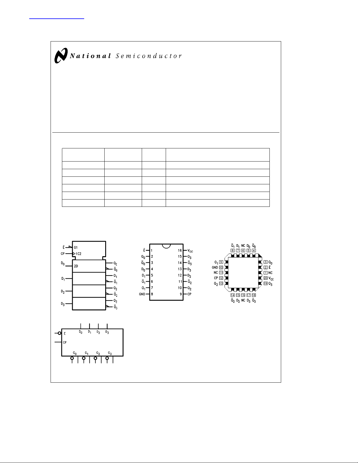
54F/74F379
Quad Parallel Register with Enable
54F/74F379 Quad Parallel Register with Enable
August 1995
General Description
The ’F379 is a 4-bit register with buffered common Enable.
This device is similar to the ’F175 but features the common
Enable rather than common Master Reset.
Commercial Military
74F379PC N16E 16-Lead (0.300×Wide) Molded Dual-In-Line
54F379DM (QB) J16A 16-Lead Ceramic Dual-In-Line
74F379SC (Note 1) M16A 16-Lead (0.300×Wide) Molded Small Outline, JEDEC
74F379SJ (Note 1) M16D 16-Lead (0.300×Wide) Molded Small Outline, EIAJ
54F379FM (QB) W16A 16-Lead Cerpack
54F379LM (QB) E20A 20-Lead Ceramic Leadless Chip Carrier, Type C
Note 1: Devices also available in 13×reel. Use suffixeSCX and SJX.
Package
Number
Logic Symbols
IEEE/IEC
Pin Assignment
DIP, SOIC and Flatpak
Features
Y
Edge triggered D-type inputs
Y
Buffered positive edge-triggered clock
Y
Buffered common enable input
Y
True and complement outputs
Y
Guaranteed 4000V minimum ESD protection
Package Description
Connection Diagrams
Pin Assignment
for LCC
TL/F/9527– 1
TL/F/9527– 5
TL/F/9527– 3
TRI-STATEÉis a registered trademark of National Semiconductor Corporation.
C
1995 National Semiconductor Corporation RRD-B30M115/Printed in U. S. A.
TL/F/9527
TL/F/9527– 2
Page 2
Unit Loading/Fan Out
54F/74F
Pin Names Description
E Enable Input (Active LOW) 1.0/1.0 20 mA/b0.6 mA
D
0–D3
CP Clock Pulse Input (Active Rising Edge) 1.0/1.0 20 mA/
Data Inputs 1.0/1.0 20 mA/b0.6 mA
Q0–Q3Flip-Flop Outputs 50/33.3b1 mA/20 mA
Q
0–Q3
Complement Outputs 50/33.3b1 mA/20 mA
U.L. Input I
HIGH/LOW Output IOH/I
IH/IIL
b
0.6 mA
OL
Functional Description
The ’F379 consists of four edge-triggered D-Type flip-flops
with individual D inputs and Q and Q
(CP) and Enable (E
When the E
) inputs are common to all flip-flops.
is input HIGH, the register will retain the present
data independent of the CP input. The D
change when the clock is in either state, provided that the
recommended setup and hold times are observed.
outputs. The Clock
and E inputs can
n
Truth Table
Inputs Outputs
E CP D
H L XNCNC
LLHH L
LLLLH
e
H
HIGH Voltage Level
e
LOW Voltage Level
L
e
Immaterial
X
e
LOW-to-HIGH Transition
L
e
No Change
NC
n
Logic Diagram
Please note that this diagram is provided only for the understanding of logic operations and should not be used to estimate propagation delays.
Q
n
Q
TL/F/9527– 4
n
2
Page 3
Absolute Maximum Ratings (Note 1)
If Military/Aerospace specified devices are required,
please contact the National Semiconductor Sales
Office/Distributors for availability and specifications.
Storage Temperature
Ambient Temperature under Bias
Junction Temperature under Bias
Plastic
Pin Potential to
V
CC
Ground Pin
Input Voltage (Note 2)
Input Current (Note 2)
Voltage Applied to Output
in HIGH State (with V
Standard Output
CC
e
TRI-STATEÉOutput
0V)
b
65§Ctoa150§C
b
55§Ctoa125§C
b
55§Ctoa175§C
b
55§Ctoa150§C
b
0.5V toa7.0V
b
0.5V toa7.0V
b
30 mA toa5.0 mA
b
0.5V to V
b
0.5V toa5.5V
Current Applied to Output
in LOW State (Max) twice the rated I
(mA)
OL
ESD Last Passing Voltge (Min) 4000V
Note 1: Absolute maximum ratings are values beyond which the device may
be damaged or have its useful life impaired. Functional operation under
these conditions is not implied.
Note 2: Either voltage limit or current limit is sufficient to protect inputs.
DC Electrical Characteristics
Symbol Parameter
V
V
V
V
V
I
IH
I
BVI
I
CEX
V
I
OD
I
IL
I
OS
I
CCL
IH
IL
CD
OH
OL
ID
Input HIGH Voltage 2.0 V Recognized as a HIGH Signal
Input LOW Voltage 0.8 V Recognized as a LOW Signal
Input Clamp Diode Voltage
Output HIGH 54F 10% V
Voltage 74F 10% V
Output LOW 54F 10% V
Voltage 74F 10% V
Input HIGH 54F 20.0
Current 74F 5.0
Input HIGH Current 54F 100
Breakdown Test 74F 7.0
Output HIGH 54F 250
Leakage Current 74F 50
Input Leakage
Test All Other Pins Grounded
Output Leakage
Circuit Current All Other Pins Grounded
Input LOW Current
Output Short-Circuit Current
Power Supply Current 28 40 mA Max V
74F 5% V
74F 4.75 V 0.0
74F 3.75 mA 0.0
Min Typ Max
2.5 I
CC
2.5 V Min I
CC
2.7 I
CC
CC
CC
b
CC
60
Recommended Operating
Conditions
Free Air Ambient Temperature
Military
Commercial 0
Supply Voltage
Military
Commercial
54F/74F
b
Units V
b
1.2 V Min I
0.5
0.5 I
CC
V Min
mA Max
mA Max
mA Max
b
0.6 mA Max V
150 mA Max V
I
V
V
V
I
V
IN
OH
OH
OH
OL
OL
ID
eb
IN
IN
OUT
e
IOD
IN
OUT
O
eb
eb
eb
e
e
e
e
e
1.9 mA
e
e
e
e
20 mA
20 mA
2.7V
7.0V
0.5V
LOW
Conditions
18 mA
V
150 mV
0V
b
55§Ctoa125§C
Ctoa70§C
§
a
4.5V toa5.5V
a
4.5V toa5.5V
1mA
1mA
1mA
CC
3
Page 4

AC Electrical Characteristics
74F 54F 74F
ea
T
25§C
Symbol Parameter V
A
ea
5.0V
CC
e
50 pF
C
L
T
A,VCC
e
C
50 pF C
L
e
Mil TA,V
e
CC
e
50 pF
L
Min Typ Max Min Max Min Max
f
t
t
max
PLH
PHL
Maximum Clock Frequency 100 140 75 100 MHz
Propagation Delay 3.5 5.0 6.5 3.0 8.5 3.5 7.5
CP to Qn,Q
n
5.0 6.5 8.5 4.0 10.0 5.0 9.5
AC Operating Requirements
74F 54F 74F
ea
25§C
T
Symbol Parameter
A
ea
CC
5.0V
V
Min Max Min Max Min Max
ts(H) Setup Time, HIGH or LOW 3.0 4.0 3.0
t
(L) Dnto CP 3.0 4.0 3.0
s
th(H) Hold Time, HIGH or LOW 1.0 2.0 1.0
t
(L) Dnto CP 1.0 2.0 1.0
h
ts(H) Setup Time, HIGH or LOW 6.0 8.0 6.0
t
(L) E to CP 6.0 8.0 6.0
s
th(H) Hold Time, HIGH or LOW 0 0 0
t
(L) E to CP 0 0 0
h
tw(H) CP Pulse Width 4.0 5.0 4.0
t
(L) HIGH or LOW 5.0 7.0 5.0
w
T
A,VCC
e
Mil TA,V
e
Com Units
CC
Com
Units
ns
ns
ns
ns
Ordering Information
The device number is used to form part of a simplified purchasing code where the package type and temperature range are
defined as follows:
74F 379 S C X
Temperature Range Family Special Variations
e
74F
Commercial QBeMilitary grade device with
e
54F
Military environmental and burn-in
Device Type
Package Code
e
Plastic DIP
P
e
Ceramic DIP
D
e
Flatpak
F
e
L
Leadless Chip Carrier (LCC)
e
S
Small Outline SOIC JEDEC
e
SJ
Small Outline SOIC EIAJ
4
processing
e
Devices shipped in 13×reel
X
Temperature Range
e
Commercial (0§Ctoa70§C)
C
e
Military (b55§Ctoa125§C)
M
Page 5

Physical Dimensions inches (millimeters)
20-Lead Ceramic Leadless Chip Carrier (L)
NS Package Number E20A
16-Lead Ceramic Dual-In-Line Package (D)
NS Package Number J16A
5
Page 6

Physical Dimensions inches (millimeters) (Continued)
16-Lead (0.150×Wide) Molded Small Outline Integrated Circuit (S)
16-Lead (0.300×Wide) Molded Small Outline Package, EIAJ (SJ)
NS Package Number M16A
NS Package Number M16D
6
Page 7

Physical Dimensions inches (millimeters) (Continued)
16-Lead (0.300×Wide) Molded Dual-In-Line Package (P)
NS Package Number N16E
7
Page 8

Physical Dimensions inches (millimeters) (Continued)
16-Lead Ceramic Flatpak (F)
NS Package Number W16A
54F/74F379 Quad Parallel Register with Enable
LIFE SUPPORT POLICY
NATIONAL’S PRODUCTS ARE NOT AUTHORIZED FOR USE AS CRITICAL COMPONENTS IN LIFE SUPPORT
DEVICES OR SYSTEMS WITHOUT THE EXPRESS WRITTEN APPROVAL OF THE PRESIDENT OF NATIONAL
SEMICONDUCTOR CORPORATION. As used herein:
1. Life support devices or systems are devices or 2. A critical component is any component of a life
systems which, (a) are intended for surgical implant support device or system whose failure to perform can
into the body, or (b) support or sustain life, and whose be reasonably expected to cause the failure of the life
failure to perform, when properly used in accordance support device or system, or to affect its safety or
with instructions for use provided in the labeling, can effectiveness.
be reasonably expected to result in a significant injury
to the user.
National Semiconductor National Semiconductor National Semiconductor National Semiconductor
Corporation Europe Hong Kong Ltd. Japan Ltd.
1111 West Bardin Road Fax: (
Arlington, TX 76017 Email: cnjwge@tevm2.nsc.com Ocean Centre, 5 Canton Rd. Fax: 81-043-299-2408
Tel: 1(800) 272-9959 Deutsch Tel: (
Fax: 1(800) 737-7018 English Tel: (
National does not assume any responsibility for use of any circuitry described, no circuit patent licenses are implied and National reserves the right at any time without notice to change said circuitry and specifications.
Fran3ais Tel: (
Italiano Tel: (
a
49) 0-180-530 85 86 13th Floor, Straight Block, Tel: 81-043-299-2309
a
49) 0-180-530 85 85 Tsimshatsui, Kowloon
a
49) 0-180-532 78 32 Hong Kong
a
49) 0-180-532 93 58 Tel: (852) 2737-1600
a
49) 0-180-534 16 80 Fax: (852) 2736-9960
 Loading...