

Datasheet 74F191SJX, 74F191SJ, 74F191SCX, 74F191SC, 74F191PC Datasheet (Fairchild Semiconductor)
...Page 1
© 1999 Fairchild Semiconductor Corporation DS009495 www.fairchildsemi.com
April 1988
Revised July 1999
74F191 Up/Down Binary Counter with Preset and Ripple Clock
74F191
Up/Down Binary Counter with Preset and Ripple Clock
General Description
The 74F191 is a reversible modulo-16 b inary coun ter featuring synchronous count ing and as ynchron ous pre settin g.
The preset featur e allows the 74F191 to be used in programmable dividers. T he Cou nt E nable in put, th e Terminal
Count output and Ripple Clock output make possible a
variety of methods of implem enti ng multista ge coun ters. In
the counting modes, state changes are i nitiated by the rising edge of the clock.
Features
■ High-Speed—125 MHz typical count frequency
■ Synchronous counting
■ Asynchronous parallel load
■ Cascadable
Ordering Code:
Devices also availab le in Tape and Reel. Specify by appending th e s uffix let t er “X” to the ordering code.
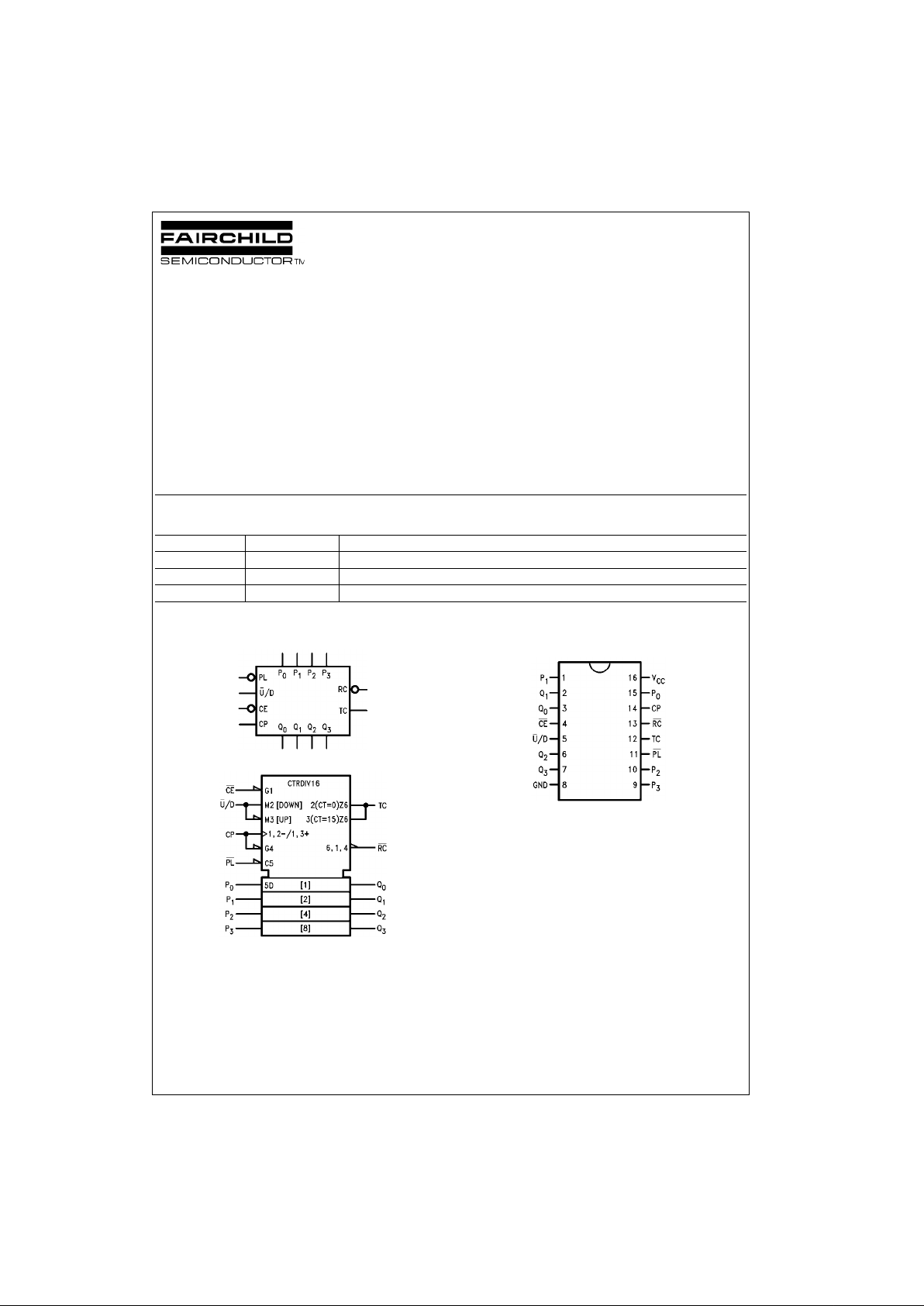
Logic Symbols
IEEE/IEC
Connection Diagram
Order Number Package Number Package Description
74F191SC M16A 16-Lead Small Outline Integrated Circuit (SOIC), JEDEC MS-012, 0.150 Narrow
74F191SJ M16D 16-Lead Small Outline Package (SOP), EIAJ TYPE II, 5.3mm Wide
74F191PC N16E 16-Lead Plastic Dual-In-Line Package (PDIP), JEDEC MS-001, 0.300 Wide
Page 2
www.fairchildsemi.com 2
74F191
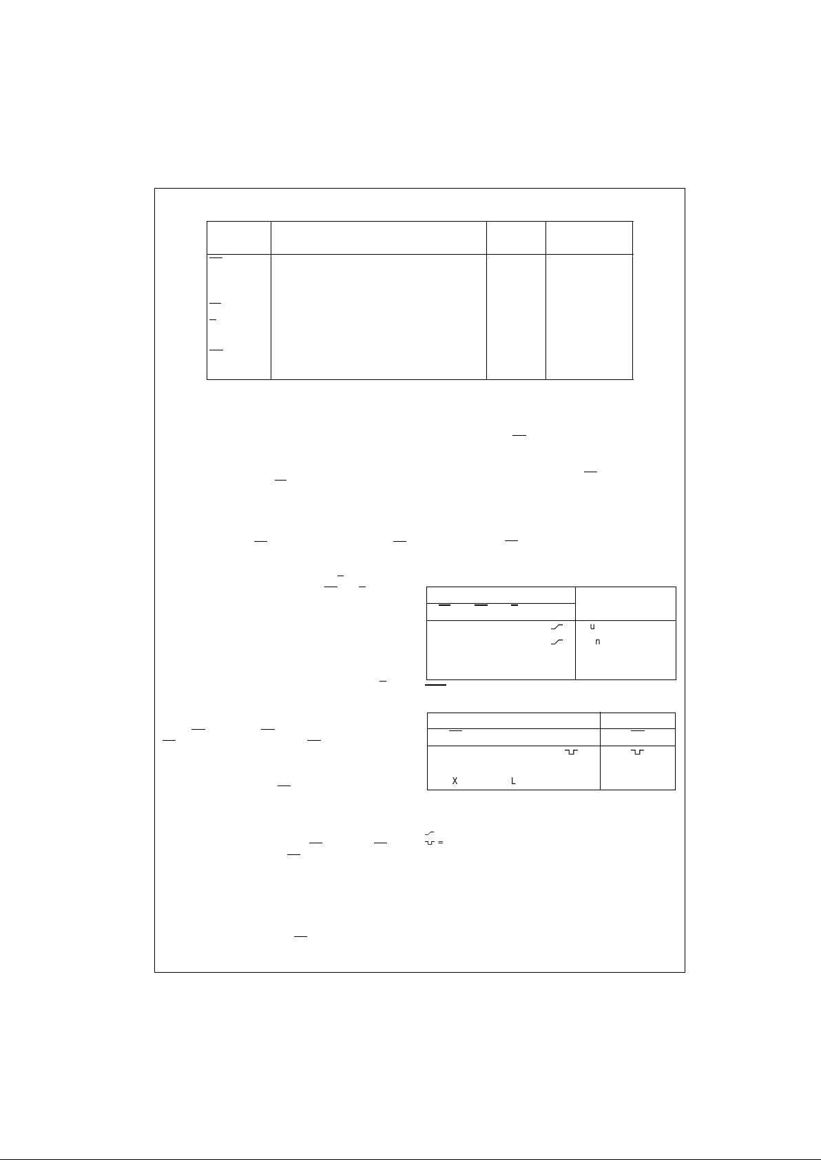
Unit Loading/Fan Out
Functional Description
The 74F191 is a synchronous up/down 4-bit binary
counter. It contains four edge-triggered flip-flops, with internal gating and s teering logic to provide individual preset,
count-up and count-down operations.
Each circuit has an asynchronous parallel load capability
permitting the counter to be preset to any desire d number.
When the Parallel Load (PL
) input is LOW, information
present on the Parallel Data inputs (P
0–P3
) is loaded into
the counter and appears on the Q outputs. T his operatio n
overrides the counting functions, as indicated in the Mode
Select Table.
A HIGH signal on the CE
input inhibits c oun ti ng . Wh en C E
is LOW, internal state changes are initiated synchronousl y
by the LOW-to-HIGH transition of the clock input. The
direction of countin g is determined by th e U
/D input signal,
as indicated in the Mode Select Table. CE
and U/D can be
changed with the clo ck in either state, provided only that
the recommended setup and hold times are observed.
Two types of outputs are pro vided as overflow/underflow
indicators. The Terminal Count (TC) output is normally
LOW and goes HIGH when a circuit reaches zero in the
count-down mo d e or r e ach es 15 in t h e c ou nt- u p mo de . T he
TC output will then remain HIGH until a state change
occurs, whether by count ing or presetting or until U
/D is
changed. The TC output should not be used as a clock signal because it is subject to decoding spikes.
The TC signal is also use d internally to ena ble the Ripple
Clock (RC
) output. The RC output is normally HIGH. When
CE
is LOW and TC is HIGH, the RC output will go LOW
when the clock next goes LOW and will stay LOW u ntil the
clock goes HIGH ag ain. This feature simplifies the desi gn
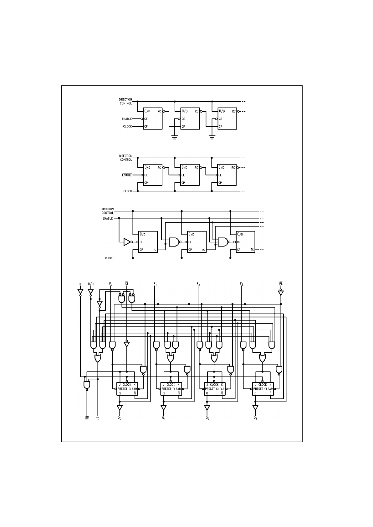
of multistage counters, as indicated in Figure 1 and
Figure 2. In Figure 1, each RC
output is used as the cl ock
input for the next higher stage. This configuration is particularly advantageous when the clock source has a limited
drive capability, since it drives only the first stage. To prevent counting in all sta ges it is onl y n ece ssar y to inh i bit th e
first stage, since a HIGH signal on CE
inhibits the R C out-
put pulse, as indicated in the RC
Truth Table. A disadvantage of this configuration, in some applications, is the
timing skew between st ate changes in the first and last
stages. This represen ts the cumulative delay of the cl ock
as it ripples through the preceding stages.
A method of causing state changes to occur simultaneously in all stages is shown in Figur e 2. All clock inputs
are driven in pa rallel and the RC
outputs propagate the
carry/borrow signals in ripple fashion. In this configuration
the LOW state du rat io n of the c lock mus t be lon g eno ugh to
allow the negative-g oin g e dge of the carry/borrow signa l to
ripple through to the last stage before the clock goes HIGH.
There is no such restriction on the HIG H state dura tion of
the clock, since the RC
output of any device goe s HIGH
shortly after its CP input goes HIGH.
The configuration shown in Figure 3 avoids ri pple delays
and their associat ed restrictio ns. The CE
input for a given
stage is formed by combinin g the TC signals from all the
preceding stages. Note that in order to inhibit countin g an
enable signal must be included in each carry gate. The
simple inhibit scheme of Figure 1 and Figure 2 doesn't
apply, because the TC output of a given stage is not
affect ed by its own CE
.
Mode Select Table
RC
Truth Table
*TC is generated internally
H = HIGH Voltage Level
L = LOW Voltage Level
X = Immaterial
= LOW-to-HIGH Clock Transition
= LOW Pulse
Pin Names Description
U.L.
Input I
IH/IIL
HIGH/LOW
Output I
OH/IOL
CE Count Enable Input (Active LOW) 1.0/3.0 20 µA/−1.8 mA
CP Clock Pulse Input (Active Rising Edge) 1.0/1.0 20 µA/−0.6 mA
P
0–P3
Parallel Data Inputs 1.0/1.0 20 µA/−0.6 mA
PL
Asynchronous Parallel Load Input (Active LOW) 1.0/1.0 20 µA/−0.6 mA
U
/D Up/Down Count Control Input 1.0/1.0 20 µA/−0.6 mA
Q
0–Q3
Flip-Flop Outputs 50/33.3 −1 mA/20 mA
RC
Ripple Clock Output (Active LOW) 50/33.3 −1 mA/20 mA
TC Terminal Count Output (Active HIGH) 50/33.3 −1 mA/20 mA
Inputs
Mode
PL
CE U/D CP
HL L
Count Up
HL H
Count Down
L X X X Preset (Asyn.)
H H X X No Change (Hold)
Inputs Output
CE
TC* CP RC
LH
HXX H
XLX H
Page 3
3 www.fairchildsemi.com
74F191
FIGURE 1. n-Stage Counter Using Ripple Clock
FIGURE 2. Synchronous n-Stage Counter Using Ripple Carry/Borrow
FIGURE 3. Synchronous n-Stage Counter with Gated Carry/Borrow
Logic Diagram
Please note that this d iagram is provided only f or t he understanding of lo gic operations and should not be used to estimat e propagation delays.
Page 4
www.fairchildsemi.com 4
74F191
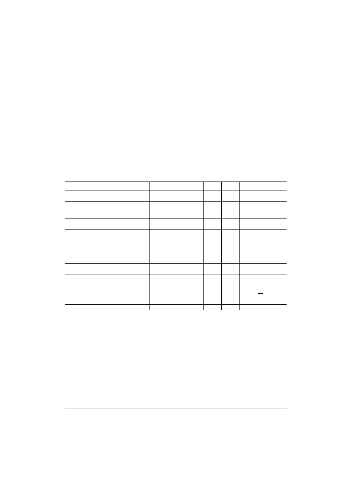
Absolute Maximum Ratings(Note 1) Recommended Operating
Conditions
Note 1: Absolute maximum ratings are values beyond which the device
may be damaged or have its useful life impaired. Functional operation
under these conditi ons is not implied.
Note 2: Either voltage limit or curren t limit is sufficient to protect in put s .
DC Electrical Characteristics
Storage Temperature −65°C to +150°C
Ambient Temperature under Bias −55°C to +125°C
Junction Temperature under Bias −55°C to +150°C
V
CC
Pin Potential to Ground Pin −0.5V to +7.0V
Input Voltage (Note 2) −0.5 V to +7.0V
Input Current (Note 2) −30 mA to +5.0 mA
Voltage Applied to Output
in HIGH State (with V
CC
= 0V)
Standard Output −0.5V to V
CC
3-STATE Output −0.5V to +5.5V
Current Applied to Output
in LOW State (Max) twice the rated I
OL
(mA)
Free Air Ambient Temperature 0°C to +70°C
Supply Voltage +4.5V to +5.5V
Symbol Parameter Min Typ Max Units
V
CC
Conditions
V
IH
Input HIGH Voltage 2.0 V Recognized as a HIGH Signal
V
IL
Input LOW Voltage 0.8 V Recognized as a LOW Signal
V
CD
Input Clamp Diode Voltage −1.2 V Min IIN = −18 mA
V
OH
Output HIGH 10% V
CC
2.5
VMin
IOH = −1 mA
Voltage 5% V
CC
2.7 IOH = −1 mA
V
OL
Output LOW 10% V
CC
0.5 V Min IOL = 20 mA
Voltage
I
IH
Input HIGH
5.0 µAMaxVIN = 2.7V
Current
I
BVI
Input HIGH Current
7.0 µAMaxVIN = 7.0V
Breakdown Test
I
CEX
Output HIGH
50 µAMaxV
OUT
= V
CC
Leakage Current
V
ID
Input Leakage
4.75 V 0.0
IID = 1.9 µA,
Test All Other Pins Grounded
I
OD
Output Leakage
3.75 µA0.0
V
IOD
= 150 mV
Circuit Current All Other Pins Grounded
I
IL
Input LOW Current −0.6
mA Max
VIN = 0.5V (except CE)
−1.8
VIN = 0.5V (CE)
I
OS
Output Short-Circuit Current −60 −150 mA Max V
OUT
= 0V
I
CC
Power Supply Current 38 55 mA Max
Page 5
5 www.fairchildsemi.com
74F191
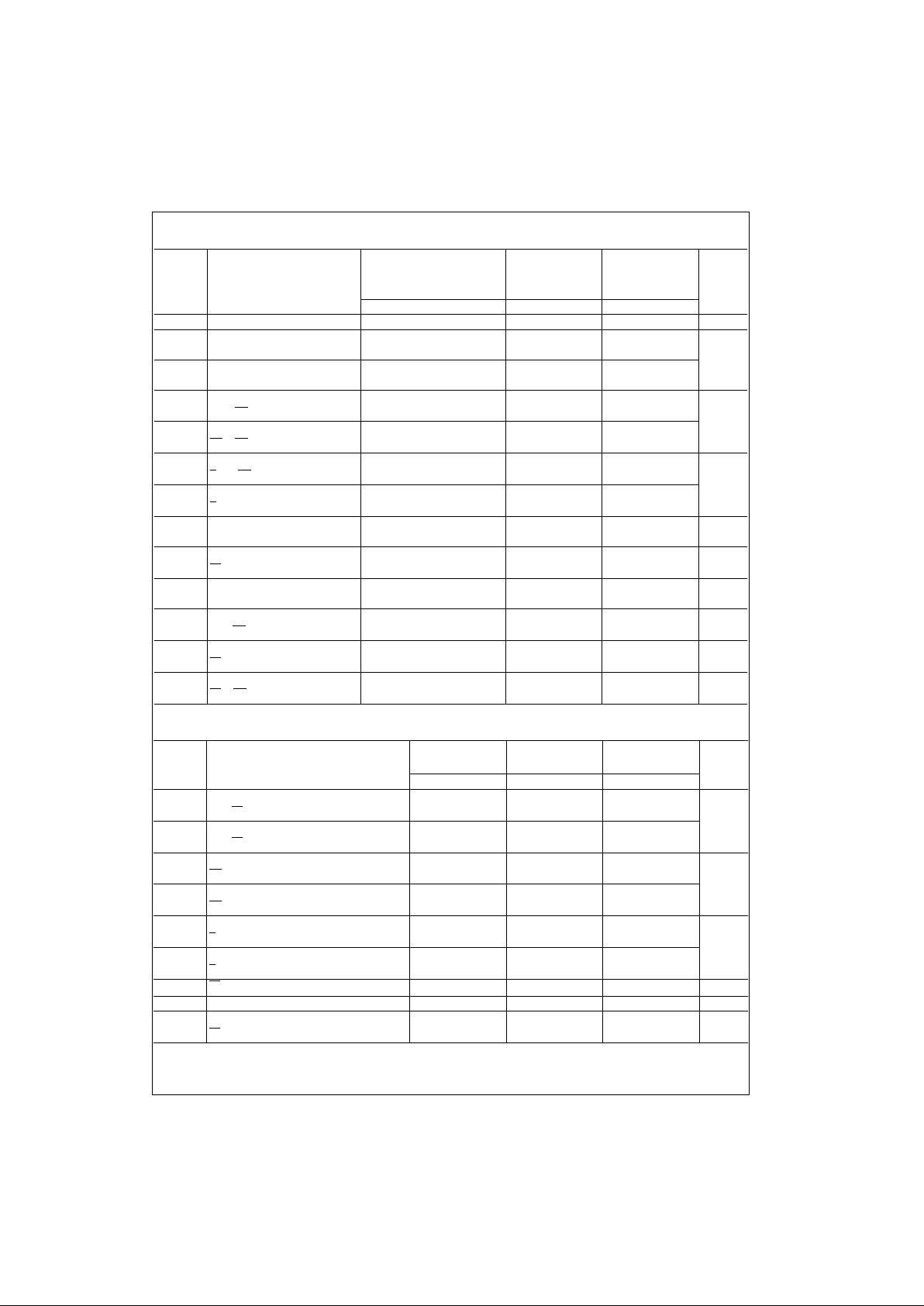
AC Electrical Characteristics
AC Operating Requirements
Symbol Parameter
TA = +25°CT
A
= −55°C to +125°CTA = 0°C to +70°C
Units
VCC = +5.0V VCC = +5.0V VCC = +5.0V
CL = 50 pF CL = 50 pF CL = 50 pF
Min Typ Max Min Max Min Max
f
MAX
Maximum Count Frequency 100 125 75 90 MHz
t
PLH
Propagation Delay 3.0 5.5 7.5 3.0 9.5 3.0 8.5
ns
t
PHL
CP to Q
n
5.0 8.5 11.0 5.0 13.5 5.0 12.0
t
PLH
Propagation Delay 6.0 10.0 13.0 6.0 16.5 6.0 14.0
t
PHL
CP to TC 5.0 8.5 11.0 5.0 13.5 5.0 12.0
t
PLH
Propagation Delay 3.0 5.5 7.5 3.0 9.5 3.0 8.5 ns
t
PHL
CP to RC
3.0 5.0 7.0 3.0 9.0 3.0 8.0
t
PLH
Propagation Delay 3.0 5.0 7.0 3.0 9.0 3.0 8.0
t
PHL
CE to RC
3.0 5.5 7.0 3.0 9.0 3.0 8.0
t
PLH
Propagation Delay 7.0 11.0 18.0 7.0 22.0 7.0 20.0 ns
t
PHL
U/D to RC
5.5 9.0 12.0 5.5 14.0 5.5 13.0
t
PLH
Propagation Delay 4.0 7.0 10.0 4.0 13.5 4.0 11.0
t
PHL
U/D to TC
4.0 6.5 10.0 4.0 12.5 4.0 11.0
t
PLH
Propagation Delay 3.0 4.5 7.0 3.0 9.0 3.0 8.0
ns
t
PHL
Pn to Q
n
6.0 10.0 13.0 6.0 16.0 6.0 14.0
t
PLH
Propagation Delay 5.0 8.5 11.0 5.0 13.0 5.0 12.0
ns
t
PHL
PL to Q
n
5.5 9.0 12.0 5.5 14.5 5.5 13.0
t
PLH
Propagation Delay 5.0 14.0 5.0 15.0
ns
t
PHL
Pn to TC 6.5 13.0 6.0 14.0
t
PLH
Propagation Delay 6.5 19.0 6.5 20.0
ns
t
PHL
Pn to RC
6.0 14.0 6.0 15.0
t
PLH
Propagation Delay 8.0 16.5 8.0 17.5
ns
t
PHL
PL to TC
6.0 13.5 6.0 14.5
t
PLH
Propagation Delay 10.0 20.0 10.0 21.0
ns
t
PHL
PL to RC
9.0 15.5 9.0 16.0
Symbol Parameter
TA = +25°CTA = −55°C to +125°CTA = 0°C to +70°C
UnitsVCC = +5.0V VCC = +5.0V VCC = +5.0V
Min Max Min Max Min Max
tS(H) Setup Time, HIGH or LOW 4.5 6.0 5.0 ns
tS(L)
Pn to PL
4.5 6.0 5.0
tH(H) Hold Time, HIGH or LOW 2.0 2.0 2.0
tH(L)
Pn to PL
2.0 2.0 2.0
tS(L) Setup Time LOW 10.0 10.5 10.0 ns
CE to CP
tH(L) Hold Time LOW 0 0 0
CE to CP
tS(H) Setup Time, HIGH or LOW 12.0 12.0 12.0 ns
tS(L)
U/D to CP
12.0 12.0 12.0
tH(H) Hold Time, HIGH or LOW 0 0 0
tH(L)
U/D to CP
000
tW(L) PL Pulse Width LOW 6.0 8.5 6.0 ns
tW(L) CP Pulse Width LOW 5.0 7.0 5.0 ns
t
REC
Recovery Time 6.0 7.5 6.0 ns
PL to CP
Page 6
www.fairchildsemi.com 6
74F191
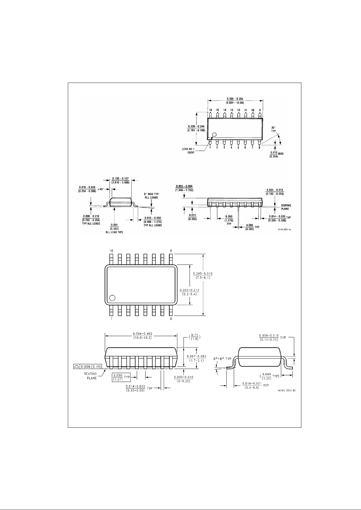
Physical Dimensions inches (millimeters) unless otherwise noted
16-Lead Small Outline Integrated Circuit (SOIC), JEDEC MS-012, 0.150 Narrow
Package Number M16A
16-Lead Small Outline Package (SOP), EIAJ TYPE II, 5.3mm Wide
Package Number M16D
Page 7
7 www.fairchildsemi.com
74F191 Up/Down Binary Counter with Preset and Ripple Clock
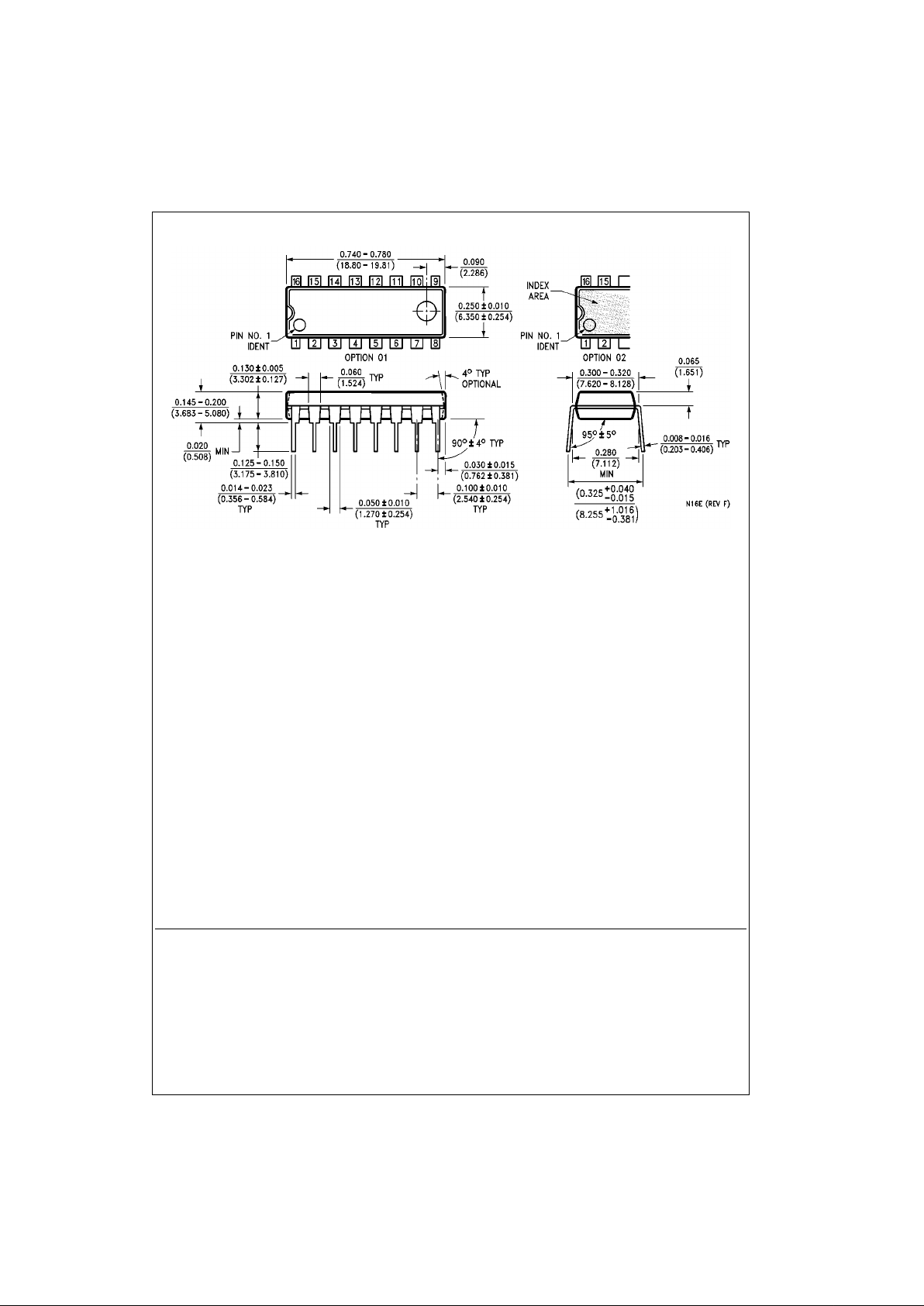
Physical Dimensions inches (millimeters) unless otherwise noted (Continued)
16-Lead Plastic Dual-In-Line Package (PDIP), JEDEC MS-001, 0.300 Wide
Package Number N16E
Fairchild does not assume any responsibility for use of any circu itry described, no circuit patent license s are implied and
Fairchild reserves the right at any time without notice to change said circuitry and specifications.
LIFE SUPPORT POLICY
FAIRCHILD’S PRODUCTS ARE NOT AUTHORIZED FOR USE AS CRITICAL COMPONENTS IN LIFE SUPPORT
DEVICES OR SYSTEMS WITHOUT THE EXPRESS WRITTEN APPROVAL OF THE PRESIDENT OF FAIRCHILD
SEMICONDUCTOR CORPORATION. As used herein:
1. Life support devices or systems are devices or systems
which, (a) are intended for surgical implant into the
body, or (b) support or sustain life, and (c) whose failure
to perform when properly used in accordance with
instructions for use provided i n the labe li ng, can be re asonably expected to result in a significant injury to the
user.
2. A critical component in any componen t of a life s uppor t
device or system whose failu re to perform can b e reasonably expected to c ause th e fa i lure of the li fe s upp or t
device or system, or to affect its safety or effectiveness.
www.fairchildsemi.com
 Loading...