

Page 1

查询N74F1763N供应商
INTEGRATED CIRCUITS
74F1763
Intelligent DRAM controller (IDC)
Product specification
Supersedes data of 1989 Nov 17
IC15 Data Handbook
1999 Jan 08
Page 2
Philips Semiconductors Product specification
74F1763Intelligent DRAM controller (IDC)
FEA TURES
•DRAM signal timing generator
•Automatic refresh circuitry
•Selectable row address hold and RAS precharge times
•Facilitates page mode accesses
•Controls 1 MBit DRAMs
•Intelligent burst-mode refresh after page-mode access cycles
ability to select the RAS
to fit the particular DRAMs being used. DTACK
from previous family parts to become a negative true, tri-stated
output. The options for latched or unlatched address are contained
on a single device by the addition of an Address Latch Enable (ALE
input. Finally , a burst refresh monitor has been added to ensure
complete refreshing after length page-mode access cycles. With a
maximum clock frequency of 100 MHz, the F1763 is capable of
controlling DRAM arrays with access times down to 40 nsec.
precharge time and Row-Address Hold time
has been modified
)
PRODUCT DESCRIPTION
The Philips Semiconductors Intelligent Dynamic RAM Controller is a
1 MBit, single-port version of the 74F1764 Dual Port Dynamic RAM
Controller. It contains automatic signal timing, address multiplexing
and refresh control required for interfacing with dynamic RAMs.
Additional features have been added to this device to take
advantage of technological advances in Dynamic RAMs. A
Page-Mode access pin allows the user to assert RAS
access cycle rather than the pre-defined four-clock-cycle pulse width
used for normal random access cycles. In addition, the user has the
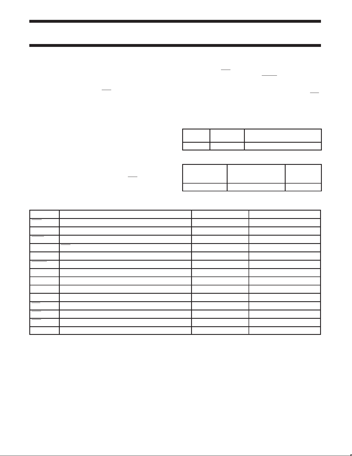
INPUT AND OUTPUT LOADING FAN-OUT TABLE
PINS
REQ DRAM Request Input 1.0/1.0
CP Clock Input 1.0/1.0
PAGE Page Mode Select Input 1.0/1.0
PRECHRG RAS Precharge Select Input 1.0/1.0
HLDROW Row Hold Select Input 1.0/1.0
DTACK Data Transfer Ack. Output 50/80 35 mA/60 mA
GNT Access Grant Output 50/80 35 mA/60 mA
RCP Refresh Clock Input 1.0/1.0
RA0–9 Row Address Inputs 1.0/1.0
CA0–9 Column Address Inputs 1.0/1.0
ALE Address Latch Enable Input 1.0/1.0
RAS Row Address Strobe Output NA 35 mA/60 mA
CAS Column Address Strobe Output NA 35 mA/60 mA
MA0–9 DRAM Address Outputs NA 35 mA/60 mA
NOTES:
One (1.0) FAST Unit Load is defined as 20 A in the HIGH state and 0.6 mA in the LOW state.
FAST Unit Loads do not correspond to DRAM Input Loads. See Functional Description for details.
DESCRIPTION 74F (U.L.) HIGH/LOW LOAD VALUE HIGH/LOW
for the entire
NO TAG
TYPE
74F1763 100 MHz 150 mA
ORDERING INFORMATION
PACKAGES
48-pin Plastic DIP N74F1763N SOT240-1
f
MAX
COMMERCIAL RANGE
TYPICAL SUPPL Y CURRENT
VCC = 5V 10%;
= 0C TO 70C
T
A
(TOTAL)
20 A/0.6 mA
20 A/0.6 mA
20 A/0.6 mA
20 A/0.6 mA
20 A/0.6 mA
20 A/0.6 mA
20 A/0.6 mA
20 A/0.6 mA
20 A/0.6 mA
PKG DWG #
1999 Jan 08 853–1406 20619
2
Page 3
Philips Semiconductors Product specification
74F1763Intelligent DRAM controller (IDC)
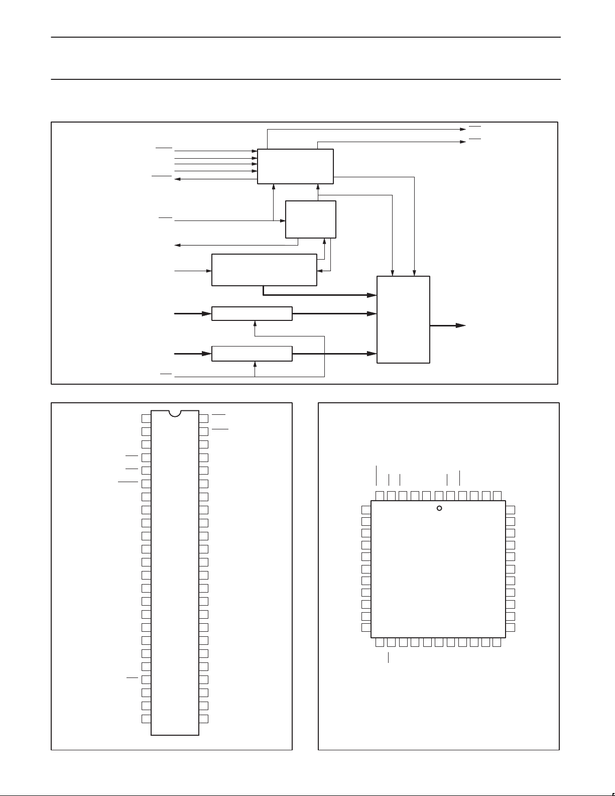
BLOCK DIAGRAM
RAS
PAGE
CP
PRECHRG
HLDROW
DTACK
RAS, CAS, MUX, DTACK
TIMING
CAS
REQ
GNT
RCP
RA0–9
CA0–9
ALE
DIP PIN CONFIGURATION
GNT
1
HLDROW
PRECHRG
2
3
4
RAS
5
CAS
6
DTACK
7
MA0
8
MA1
9
MA2
10
MA3
11
GND
12 37
GND
13
GND
14
GND
15
MA4
16
MA5
17
MA6
18 31
MA7
19 30
MA8
20
MA9
21
ALE
22
CA9
23
RA9
24 25
CA8
BURST REFRESH MONITOR
REFRESH ADDRESS COUNTER
ROW ADDRESS LATCH
COLUMN ADDR. LATCH
REQ
48
47
PAGE
46
CP
45
RCP
44
RA0
43
CA0
42
RA1
CA1
41
40
RA2
39
CA2
38
V
CC
V
CC
36
V
CC
RA3
35
34
CA3
RA4
33
32
CA4
RA5
CA5
29
RA6
28
CA6
27
RA7
26
CA7
RA8
REFRESH
ARBITRATION
MULTIPLEXER
PLCC PIN CONFIGURA TION
DTACK
6
7
MA0
8
MA1
9
MA2
10
MA3
11
GND
12
GND
13
MA4
MA5
14
MA6
15
16
MA7
17
MA8
18 19 20 21 22 24 25 26 27 28
MA9
MA0–9
SF01400
CAS
RAS
PRECHRG
HLDROW
5 4 32 144 43 42 41 40
ALE
CA9
RA9
CA8
PAGECPRCP
GNT
REQ
23
RA8
CA7
RA7
CA6
RA6
RA0
CA5
39
CA0
38
RA1
37
CA1
36
RA2
35
CA2
34
V
CC
33
RA3
32
CA3
31
RA4
30
CA4
29
RA5
1999 Jan 08
SF01401
SF01402
3
Page 4
Philips Semiconductors Product specification
SYMBOL
TYPE
NAME AND FUNCTION
74F1763Intelligent DRAM controller (IDC)
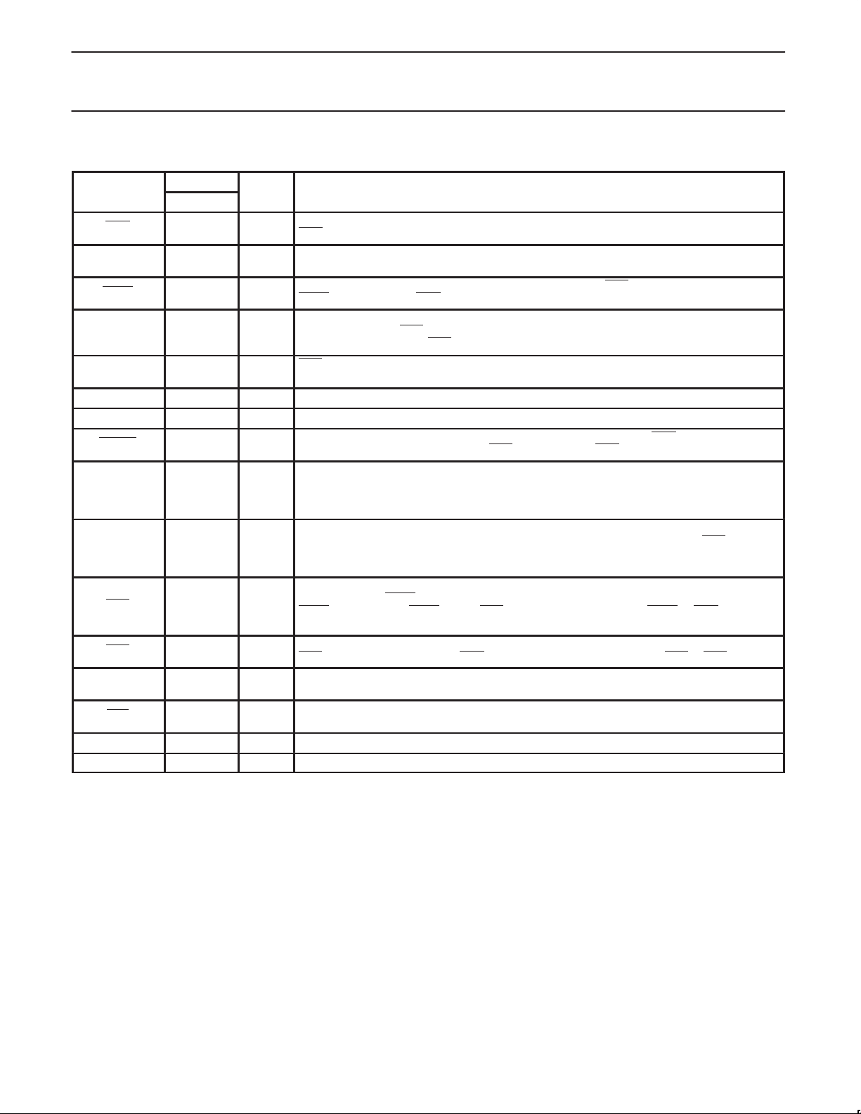
PIN DESCRIPTION
PINS
DIP
REQ 48 Input
GNT 1 Output
PAGE 47 Input
HLDROW 2 Input
PRECHRG 3 Input
CP 46 Input Clock input. Used by the Controller for all timing and arbitration functions.
RCP 45 Input Refresh Clock input. Divided internally by 64 to produce an internal Refresh Request.
DTACK 6 Output
44, 42, 40,
RA0–9
CA0–9
RAS 4 Output
CAS 5 Output
MA0–9
ALE 21 Input
V
CC
GND 11–14 Ground
35, 33, 31,
29, 27, 25,
23
43, 41, 39,
34, 32, 30,
28, 26, 24,
22
7–10,
15–20
36–38 +5V 10% Supply voltage.
Inputs Row Address inputs.
Inputs
Output
Active Low Memory Access Request input, must be asserted for the entire DRAM access cycle.
REQ is sampled on the rising edge of the CP clock.
Active High Grant output. When High indicates that a DRAM access (inactive during refresh)
cycle has begun. Asserted from the rising edge of the CP clock.
Active Low Page-Mode Access input. Forces the IDC to keep RAS asserted for as long as the
PAGE input is Low and REQ is asserted Low.
Row Address Hold input. If Low will configure the IDC to maintain the row addresses for a full
CP clock cycle after RAS is asserted. If High will program the IDC to maintain row addresses for
a 1/2 CP clock cycle after RAS
RAS Precharge input. A Low will program the IDC to guarantee a minimum of 4 CP clock cycles
of precharge. A High will guarantee 3 clock cycles of precharge.
Active Low, 3-state Data T ransfer Acknowledge output. Enabled by the REQ input and asserted
four clock cycles after the assertion of RAS, 3-stated when REQ goes High.
Column Address inputs. Propagated to the MA0–9 outputs 1 CP clock cycle after RAS is
asserted, if HLDROW = 0 or 1/2 clock cycle later if HLDROW is 1.
Active Low Row Address Strobe. Asserted for four clock cycles during each refresh cycle
regardless of the PAGE input. Also asserted for four clock cycles during processor access if the
PAGE
input is High. If PAGE is Low, RAS is negated upon negation of PAGE or REQ, whichever
occurs first.
Active Low Column Address Strobe. Always asserted 1.5 CP clock cycles after the assertion of
RAS. Negated upon negation of REQ. HLDROW input pin does not affect RAS to CAS timing.
DRAM multiplexed address outputs. Row and column addresses asserted on these pins during
an access cycle. Refresh counter addresses presented on these outputs during refresh cycles.
Active Low Address Latch Enable input. A Low on this pin will cause the address latches to be
transparent. A High level will latch the RA0–9 and CA0–9 inputs.
is asserted.
1999 Jan 08
4
Page 5

Philips Semiconductors Product specification
74F1763Intelligent DRAM controller (IDC)
FUNCTIONAL DESCRIPTION
The 74F1763 1 Megabit Intelligent DRAM Controller (IDC) is a
synchronous device with most signal timing being a function of the
CP input clock.
Arbitration
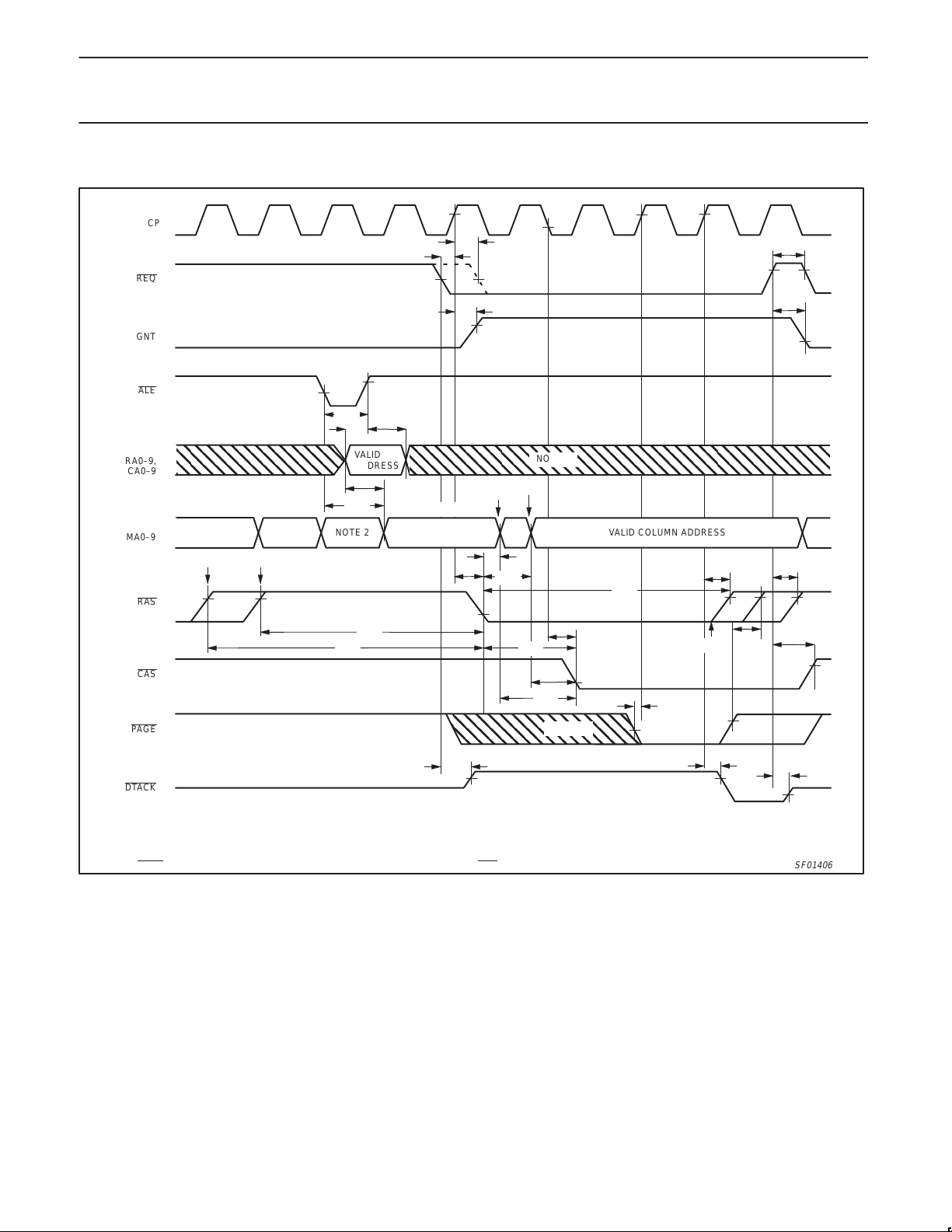
Once the DRAM’s RAS precharge time has been satisfied, the REQ
input is sampled on each rising edge of the CP clock and an
internally generated refresh request is sampled on each falling edge
of the same clock. When only one of these requests is sampled as
active the appropriate memory cycle will begin immediately. For a
memory access cycle this will be indicated by GNT and RAS
both being asserted and for a refresh cycle by multiplexing refresh
address to the MA0–9 outputs and subsequent assertion of RAS
after 1/2CP clock cycle. If both memory access and refresh requests
are active at a given time the request sampled first will begin
immediately and the other request (if still asserted) will be serviced
upon completion of the current cycle and it’s associated RAS
precharge time.
outputs
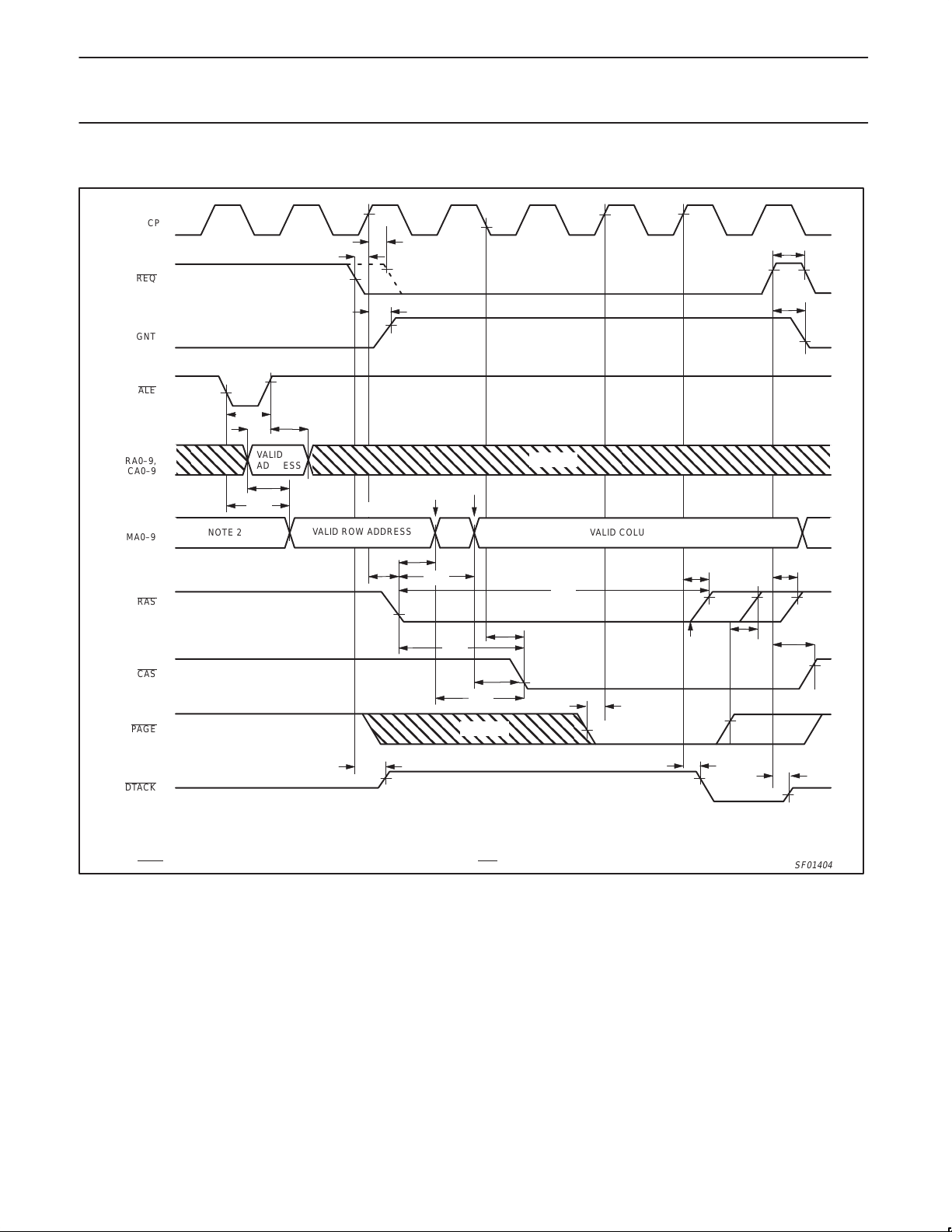
Memory access
The row (RA0–9) and column (CA0–9) address inputs are latched
when ALE
propagate directly to the outputs. When GNT and RAS
after a REQ
already propagated to the MA0–9 outputs for the row address. One
or one-half CP clock cycles later (depending on the state of the
HLDROW input) the column address (CA0–9) inputs are propagated
to the MA0–9 outputs. CAS
clock cycles after RAS
will be negated approximately four CP clock cycles after its initial
assertion. At this time the DTACK
the completion of a memory access cycle. The IDC will maintain the
state of all its outputs until the REQ
waveforms).
input is High. When ALE is Low the input addresses
are asserted,
has been sampled the RA0–9 address inputs will have
is always asserted one and one-half CP
is asserted. If the PAGE input is High, RAS
output becomes valid indicating
input is negated ( see timing
Row address hold times
If the HLDROW input of the IDC is High the row address outputs will
remain valid 1/2 CP clock cycle after RAS
HLDROW input is Low the row address outputs will remain valid one
CP clock cycle after RAS
is asserted.
is asserted. If the
RAS precharge timing
In order to meet the RAS precharge requirement of dynamic RAMs,
the controller will hold-off a subsequent RAS
a processor access request or a refresh cycle for four or three full
CP clock cycles from the previous negation of RAS
the state of the PRECHRG input. If the PRECHRG input is Low,
RAS
remains High for at least 4 CP clock cycles. If the PRECHRG
input is High RAS
remains High for at least 3 CP clock cycles.
signal assertion due to
, depending on
Refresh timing
The refresh address counter wakes-up in an all 1’s state and is an
up counter. The refresh clock (RCP) is internally divided down by 64
to produce an internal refresh request. This refresh request is
recognized either immediately or at the end of a running memory
access cycle. Due to the possibility that page mode access cycles
may be lengthy, the controller keeps track of how many refresh
requests have been missed by logging them internally (up to 128)
and servicing any pending refresh requests at the end of the
memory access cycle. The controller performs RAS
cycles until all pending refresh requests are depleted.
-only refresh
Page-mode access
Fast accesses to consecutive locations of DRAM can be realized by
asserting the PAGE
mode, the controller does not automatically negate RAS
CP clock cycles, but keeps it asserted throughout the access cycle.
By using external gates, the CAS
while changing the column address inputs to the controller, which
will propagate to the MA
column address. This is only useful if the ALE
the user to charge addresses. This mode can be used with DRAMs
that support page or nibble mode addressing.
input as shown in the timing waveforms. In this
after four
output can be gated on and off
–MA9 address outputs and provide a new
0
input is Low, enabling
Output driving characteristics
Considering the transmission line characteristic of the DRAM arrays,
the outputs of the IDC have been designed to provide incident-edge
switching (in Dual-Inline-Packaged memory arrays), needed in high
performance systems. For more information on the driving
characteristics, please refer to Philips Semiconductors application
note AN218. The driving characteristics of the 74F1763 are the
same as those of the 74F765 shown in the application note.
1999 Jan 08
5
Page 6
Philips Semiconductors Product specification
SYMBOL
PARAMETER
UNIT
1
SYMBOL
PARAMETER
TEST CONDITIONS
1
UNIT
V
CC
MIN
I
mA
V
MIN
V
CC
MIN
I
mA
V
MIN
74F1763Intelligent DRAM controller (IDC)
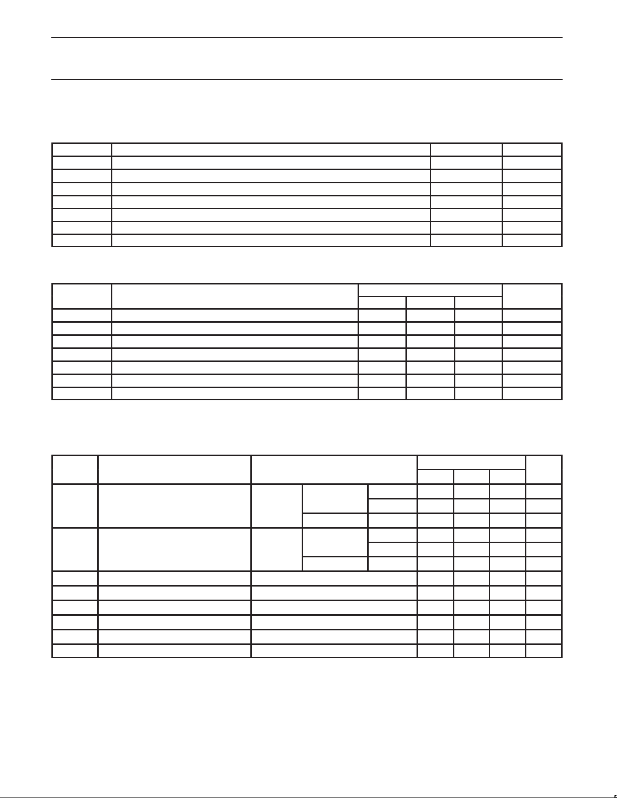
ABSOLUTE MAXIMUM RATINGS
Operation beyond the limits set forth in this table may impair the useful life of the device. Unless otherwise noted, these limits are over the
operating free-air temperature range.
SYMBOL
V
T
V
V
I
OUT
I
OUT
T
STG
CC
IN
IN
A
Supply voltage –0.5 to +7.0 V
Input voltage –0.5 to +7.0 V
Input current –30 to +5 mA
Voltage applied to output in High output state –0.5 to +V
Current applied to output in Low output state 120 mA
Operating free-air temperature range 0 to +70
Storage temperature –65 to +150
RECOMMENDED OPERATION CONDITIONS
V
CC
V
IH
V
IL
I
IK
I
OH
I
OL
T
A
NOTE:
1. Transient currents will exceed these values in actual operation.
Supply voltage 4.5 5.0 5.5 V
High-level input voltage 2.0 V
Low-level input voltage 0.8 V
Input clamp current –18 mA
High-level output current
Low-level output current
1
1
Operating free-air temperature range 0 70
PARAMETER RATING UNIT
CC
V
C
C
LIMITS
MIN NOM MAX
–15 mA
24 mA
C
DC ELECTRICAL CHARACTERISTICS
Over recommended operating free-air temperature range unless otherwise noted.
LIMITS
MIN TYP
=
=
,
= –15
V
V
V
I
I
I
I
High-level output voltage
OH
Low-level output voltage
OL
Input clamp voltage VCC = MIN, II = I
IK
I
Input current at maximum input voltage VCC = 0.0V, VI = 7.0V 100
I
High-level input current VCC = MAX, VI = 2.7V 20
IH
Low-level input current VCC = MAX, VI = 0.5V –0.6 mA
IL
Output current
OS
Supply current (total) VCC = MAX 220 mA
CC
5
VIL = MAX,
=
IH
=
=
V
= MAX,
IL
=
IH
VCC = MAX, VO = 2.25V –100 –225 mA
OH
3
I
= –35 mA 5% V
OH2
,
= 24
OL
4
I
= 60 mA 5% V
OL2
IK
10% V
5% V
10% V
5% V
2.5 V
CC
2.7 3.4 V
CC
2.4 V
CC
CC
CC
CC
NOTES:
1. For conditions shown as MIN or MAX, use the appropriate value specified under recommended operating conditions for the applicable type.
2. All typical values are at V
is transient current necessary to guarantee a Low to High transition in a 70W transmission line.
3. I
OH2
is transient current necessary to guarantee a High to Low transition in a 70W transmission line.
4. I
OL2
5. Not more than one output should be shorted at a time. For testing I
= 5V, T
CC
techniques are preferable in order to minimize internal heating and more accurately reflect operational values. Otherwise, prolonged
= 25C.
A
, the use of high-speed test apparatus and/or sample-and-hold
OS
shorting of a High output may raise the chip temperature well above normal and thereby cause invalid readings in other parameter tests. In
any sequence of parameter tests, I
tests should be performed last.
OS
2
MAX
0.35 0.50 V
0.35 0.50 V
0.35 0.80 V
–0.73 –1.2 V
mA
mA
1999 Jan 08
6
Page 7
Philips Semiconductors Product specification
74F1763Intelligent DRAM controller (IDC)
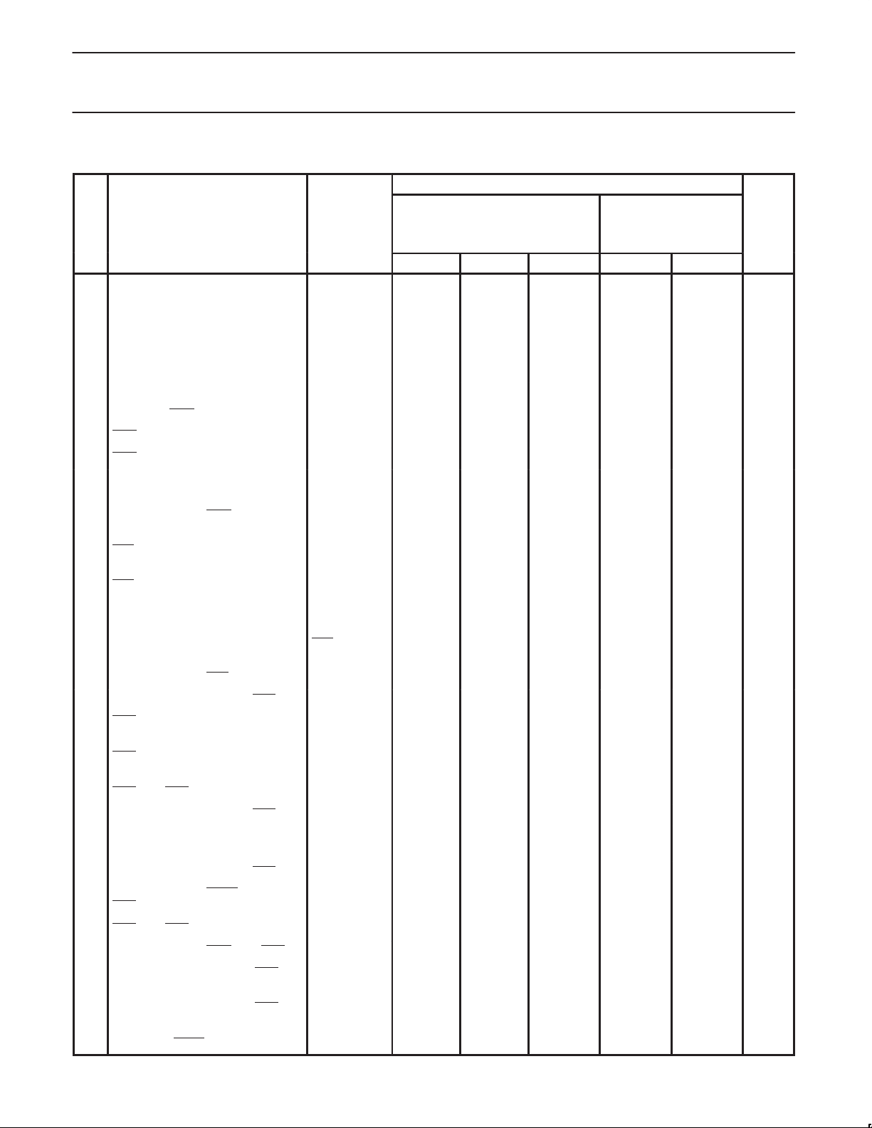
AC ELECTRICAL CHARACTERISTICS
LIMITS
TA = 25C
NO PARAMETER
TEST
CONDITIONS
VCC = +5.0V 10%
C
= 300pF
L
= 70
R
L
MIN TYP MAX MIN MAX
1 CP clock period (tcp) 10 10 ns
2 CP clock low time 5 5 ns
3 CP clock high time 5 5 ns
4 RCP clock period 100 100 ns
5 RCP clock low time 10 10 ns
6 RCP clock high time 10 10 ns
7
Setup time REQ() to CP()
8
REQ High hold time after CP()
9 REQ High pulse width
10
Propagation delay CP() to GNT
1
2
4 2 4 ns
0 0 ns
1/2tcp + 5 1/2tcp + 5 1/2tcp + 5 1/2tcp + 5 1/2tcp + 5 ns
8.5 11 13.5 8.5 15.5 ns
High
11
Propagation delay REQ() to GNT
8.5 10.5 13 8.5 14 ns
Low
12 ALE pulse width Low 4 1 4 ns
13 RA0–9, CA0–9 High or Low setup to
ALE
()
14
ALE() to RA0–9, CA0–9 High or
2 0 2 ns
1 0 1 ns
Low hold
15 Propagation delay RA0–9, CA0–9
High or Low to MA0–9
16
Propagation delay ALE() to MA0–9
17
Propagation delay CP() to RAS()
18
RAS() to MA0–9 (column address)
3
ALE Low 4 7.5 11 4 14 ns
5.5 8.5 13 5.5 15 ns
8.5 10.5 12.5 8.5 14 ns
HLDROW = 1 1/2tcp – 2 1/2tcp + 2 1/2tcp + 5.5 1/2tcp – 2.5 1/2tcp + 7 ns
skew
19
RAS() to MA0–9 (column address)
HLDROW = 0 1tcp – 2 1tcp + 2 1tcp + 5.5 1tcp – 2.5 1tcp + 7 ns
skew
20
RAS() to RAS() skew
21
Propagation delay CP() to RAS()
22
Propagation delay REQ() to
4
RAS()
23
Propagation delay CP() to CAS()
24
Propagation delay PAGE() to
4
()
RAS
25
RAS() to CAS() skew
26
Propagation delay REQ() to CAS()
27
MA0–9 (column address) to CAS()
PAGE = 1 4tcp + 1.5 4tcp + 3.5 4tcp + 6 4tcp + 1 4tcp + 6.5 ns
12 14 16.5 12 18.5 ns
14.5 17.5 20 14 24 ns
6 8 10 6 11 ns
10 12.5 15 10 17 ns
1.5tcp–4.5 1.5tcp–2.5 1.5tcp–0.5 1.5tcp–5.5 1.5tcp ns
10 12 15 10 17 ns
1tcp – 8 1tcp – 4 1tcp – 0.5 1tcp – 9 1tcp – 0.5 ns
skew
28
MA0–9 (column address) to CAS()
HLDROW = 0 1/2tcp – 8 1/2tcp – 4 1/2tcp – 0.5 1/2tcp – 9 1/2tcp – 0.5 ns
skew
29
Set-up time PAGE() to CP()
2 2 ns
TA = 0C to +70C
VCC = +5.0V 10%
C
= 300pF
L
RL = 70
UNIT
1999 Jan 08
7
Page 8
Philips Semiconductors Product specification
74F1763Intelligent DRAM controller (IDC)
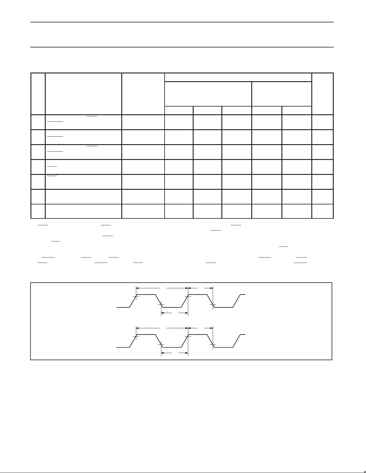
AC ELECTRICAL CHARACTERISTICS (Continued)
LIMITS
TA = 25C
NO PARAMETER
TEST
CONDITIONS
VCC = +5.0V 10%
C
= 300pF
L
= 70
R
L
MIN TYP MAX MIN MAX
30
Propagation delay REQ() to
DTACK
()
31
Propagation delay CP() to
DTACK
()
32
Propagation delay REQ() to
6 8 11.5 6 12 ns
7.5 9.5 12 7.5 13 ns
9 12 13 9 15.5 ns
DTACK (3-state)
33 MA0–9 (refresh address) to
RAS
() skew
34
RAS() to MA0–9 (refresh
1/2tcp – 5 1/2tcp – 6.5 ns
1tcp – 2 1tcp – 2.5 ns
address) skew
35
RAS() to RAS() skew
PRECHRG = 0 4tcp – 6 4tcp – 3.5 4tcp – 1.5 4tcp – 6.5 4tcp – 6.5 ns
(precharge)
36
RAS() to RAS() skew
PRECHRG = 1 3tcp – 6 3tcp – 3.5 3tcp – 1.5 3tcp + 1 3tcp – 6.5 ns
(precharge)
NOTES:
1. REQ
High hold means that, if REQ is High at the rising clock edge, it is guaranteed that the REQ input was not sampled as Low.
2. A 50% duty cycle clock is recommended. If the duty cycle of the clock is not 50%, REQ
falling CP clock edge samples REQ
3. When ALE
is Low, the address input latches are in the transparent mode and therefore any changes in the address inputs will be propagated
as High. This is to ensure that refresh cycles don’t get locked-up.
should be held high for enough time such that a
to the MA0–9 outputs. Figure 2 illustrates RA0–9 inputs propagating to the MA0–9 outputs, but later in the cycle, if ALE
CA0–9 inputs are multiplexed to the MA0–9 outputs the CA0–9 inputs will be in the transparent mode.
4. If PAGE
is High and REQ is Low, RAS is automatically negated after approximately 4 CP clock cycles. If PAGE is Low and REQ is also Low,
RAS
will be negated when PAGE goes High. RAS will always be negated when REQ goes High regardless of the state of PAGE input.
TA = 0C TO +70C
VCC = +5.0V 10%
C
= 300pF
L
RL = 70
is still Low when the
UNIT
TIMING DIAGRAMS
CP
RCP
1
2
4
5
3
6
Figure 1. Clock cycle timing
SF01403
1999 Jan 08
8
Page 9
Philips Semiconductors Product specification
74F1763Intelligent DRAM controller (IDC)
TIMING DIAGRAMS (Continued)
CP
REQ
GNT
ALE
8
7
10
12
14
13
9
11
16
3-STATE
VALID
ADDRESS
15
HLDROW = 1
VALID ROW ADDRESS
17
30
HLDROW = 0
18
19
25
27
NOTE 3
RA0–9,
CA0–9
MA0–9
RAS
CAS
PAGE
DTACK
NOTE 1: If the RA0–9 and CA0–9 address inputs are not latched, RA0–9 inputs should remain valid until row address hold time is met and CA0–9 inputs should remain valid until column
address hold time is met.
NOTE 2: MA0–9 outputs will contain the present row address on the RA0–RA9 inputs or the last row address latched into the device.
NOTE 3: PAGE input may be asserted anytime before this rising clock edge in order to hold RAS low.
NOTE 2
NOTE 1
VALID COLUMN ADDRESS
21
20
23
PAGE = 1
28
29
31
22
24
26
32
3-STATE
SF01404
Figure 2. Memory access cycle timing
1999 Jan 08
9
Page 10
Philips Semiconductors Product specification
74F1763Intelligent DRAM controller (IDC)
TIMING DIAGRAMS (Continued)
CP
REQ
GNT
ALE
RA0–9,
CA0–9
MA0–9
RAS
CAS
PRECHRG = 1 PRECHRG = 0
NOTE 4
REFRESH
ADDR.
33
35
PRECHRG = 1 PRECHRG = 1PRECHRG = 0 PRECHRG = 0
34
REFRESH
ADDR.
33
NOTE 1
NOTE 2
NOTE 3
NEXT REFRESH ADDRESS
34
20
2036
DTACK
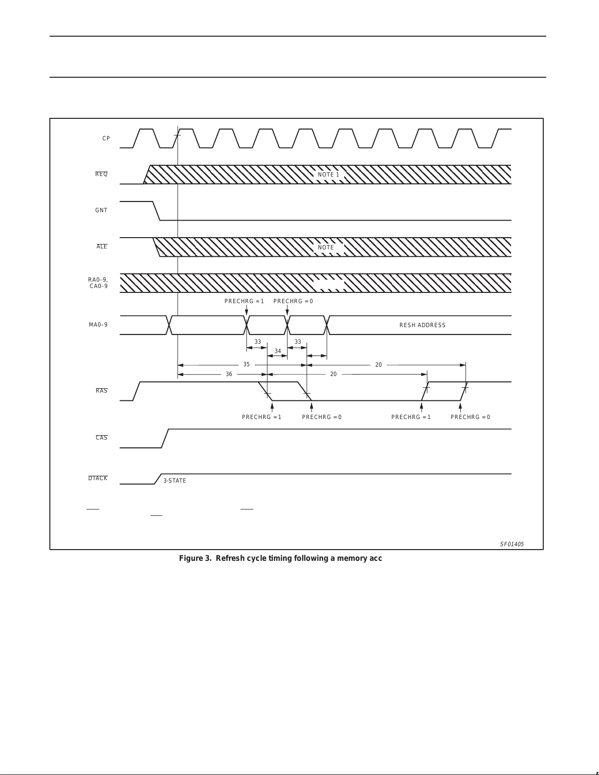
NOTE 1: REQ input is a don’t care during a memory refresh cycle. If REQ is asserted during a refresh cycle, it will be recognized at the first rising CP clock edge, following the refresh
cycle and its associated RAS
NOTE 2: RA0–9 and CA0–9 address inputs may be latched at anytime during a memory refresh cycle. However, a memory access cycle will not begin until after the completion of the
refresh cycle.
NOTE 3: RA0–9 and CA0–9 if in the transparent mode do not propogate to the MA0–9 outputs during a refresh cycle.
NOTE 4: MA0–9 output will contain the present row address on the RA0–RA9 inputs or the last row address latched into the device.
3-STATE
precharge time (see Figure 4).
SF01405
Figure 3. Refresh cycle timing following a memory access cycle
1999 Jan 08
10
Page 11
Philips Semiconductors Product specification
74F1763Intelligent DRAM controller (IDC)
TIMING DIAGRAMS (Continued)
CP
REQ
GNT
ALE
8
7
10
12
14
13
9
11
RA0–9,
CA0–9
3-STATE
REFRESH
ADDRESS
MA0–9
RAS
CAS
PAGE
DTACK
NOTE 1: If the RA0–9 and CA0–9 address inputs are not latched, RA0–9 inputs should remain valid until row address hold time is met and CA0–9 inputs should remain valid until column
address hold time is met.
NOTE 2: MA0–9 outputs will contain the present row address on the RA0–RA9 inputs or the last row address latched into the device.
NOTE 3: PAGE input may be asserted anytime before this rising clock edge in order to hold RAS low.
REFRESH
ADDRESS
PRECHRG = 0 PRECHRG = 1
VALID
ADDRESS
16
NOTE 2
35
15
VALID ROW ADDRESS
36
HLDROW = 0
HLDROW = 1
17
30
18
NOTE 1
VALID COLUMN ADDRESS
19
23
25
28
27
NOTE 3
20
29
21
PAGE = 1
31
22
24
26
32
3-STATE
SF01406
Figure 4. Memory access cycle timing following a refresh cycle
1999 Jan 08
11
Page 12
Philips Semiconductors Product specification
74F1763Intelligent DRAM controller (IDC)
PU
1, 7, 9, 10
33.34 MHz
CP
F160A
Q0 Q2
16.67 MHz
CPU CLOCK
MEMORY
SELECT
(FROM ADDRESS DECODER
AS
A3
A2
A4–A12
A13–A21
A0
A1
SIZ0
SIZ1
DCQ
D
CQ
PU
PRECHRG
HLROW
REQ
PAGE
ALE
CA9
RA9
RA0–8
CA0–8
PLD
10
CP RCP
74F1763
DRAM
CONTROLLER
MA0–MA9
RAS
CAS
RAS
MA0–MA9
CAS0
CAS1
CAS2
CAS3
STERM
DCQ
Q
DS Q3
CBACK
CBREQ
DSACK0
DSACK1
CP
F164
MR
DCQ
SF01407
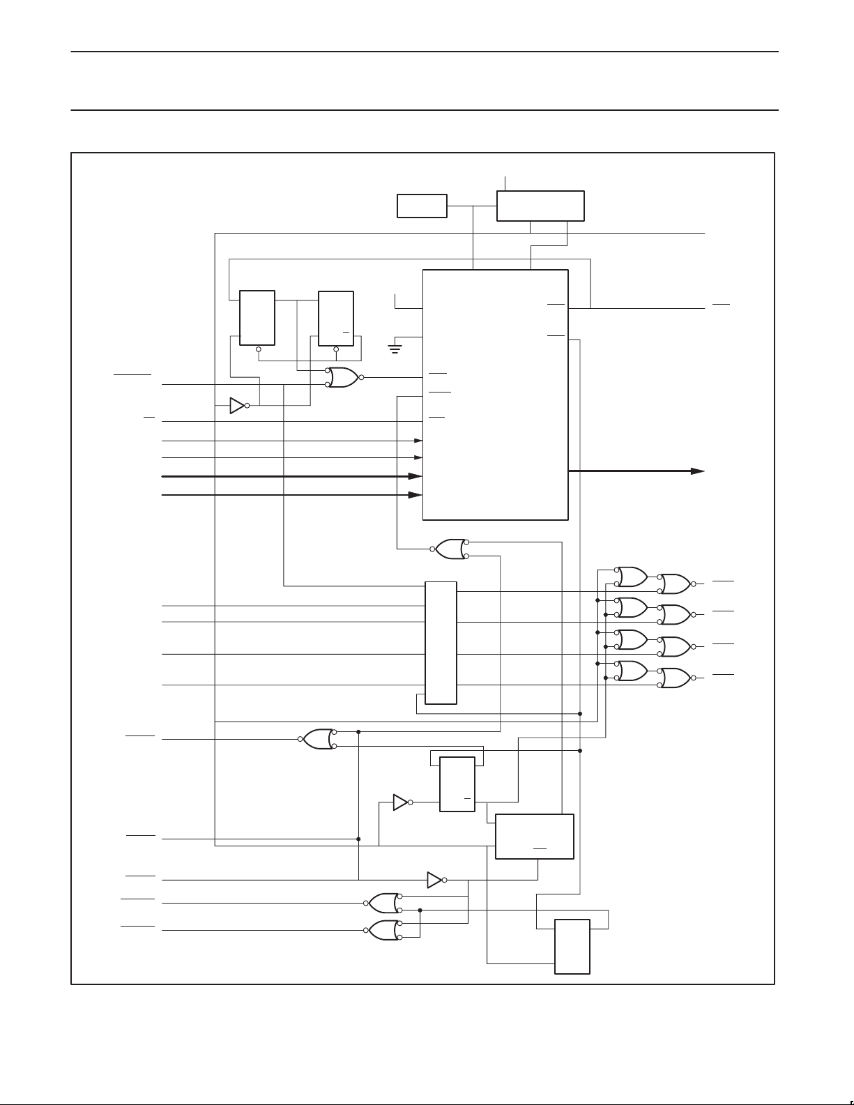
Figure 5. 16.67 MHz 68030 interface with 74F1763 for cache burst mode support using 4Mbytes of 100nsec. nibble-mode DRAMs
(Four 32 bit words read to or written from cache in only clock cycles
1999 Jan 08
12
Page 13
Philips Semiconductors Product specification
74F1763Intelligent DRAM controller (IDC)
TEST CIRCUIT AND WAVEFORMS
V
CC
PULSE
GENERATOR
V
IN
R
T
D.U.T.
V
OUT
R
L
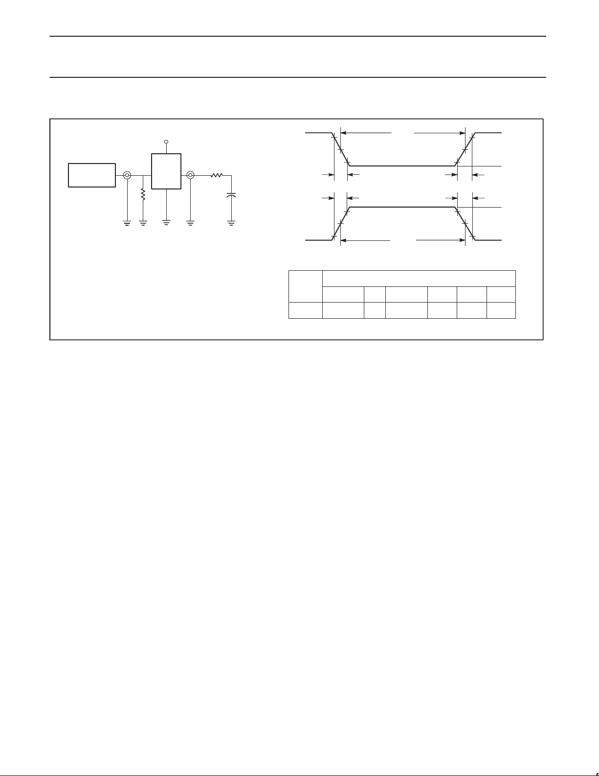
Test Circuit Simulating RAM Boards
DEFINITIONS:
= Load resistor; see AC CHARACTERISTICS for value.
R
L
C
= Load capacitance includes jig and probe capacitance;
L
see AC CHARACTERISTICS for value.
R
= Termination resistance should be equal to Z
T
pulse generators.
C
L
OUT
of
NEGATIVE
PULSE
POSITIVE
PULSE
Family
74F
90%
10%
Amplitude
3.0V
t
w
V
M
10%
)
t
THL (tf
)
t
TLH (tr
90%
V
M
t
t
t
w
TLH (tr
THL (tf
10%
)
)
90%
V
M
V
Input Pulse Definition
INPUT PULSE REQUIREMENTS
V
M
1.5V
Rep. Rate
1MHz 500ns
t
w
90%
M
10%
t
TLHtTHL
2.5ns 2.5ns
AMP (V)
0V
AMP (V)
0V
SF01408
1999 Jan 08
13
Page 14
Philips Semiconductors Product specification
74F1763Intelligent DRAM controller (IDC)
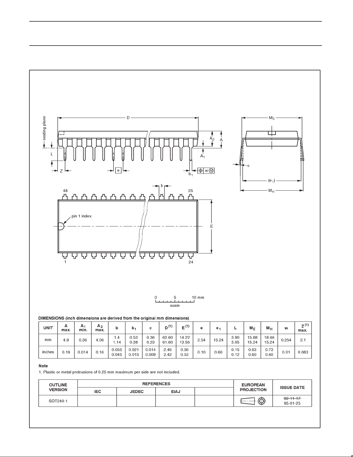
DIP48: plastic dual in-line package; 48 leads (600 mil) SOT240-1
1999 Jan 08
14
Page 15

Philips Semiconductors Product specification
74F1763Intelligent DRAM controller (IDC)
NOTES
1999 Jan 08
15
Page 16

Philips Semiconductors Product specification
74F1763Intelligent DRAM controller (IDC)
Data sheet status
Data sheet
status
Objective
specification
Preliminary
specification
Product
specification
Product
status
Development
Qualification
Production
Definition
This data sheet contains the design target or goal specifications for product development.
Specification may change in any manner without notice.
This data sheet contains preliminary data, and supplementary data will be published at a later date.
Philips Semiconductors reserves the right to make chages at any time without notice in order to
improve design and supply the best possible product.
This data sheet contains final specifications. Philips Semiconductors reserves the right to make
changes at any time without notice in order to improve design and supply the best possible product.
[1]
[1] Please consult the most recently issued datasheet before initiating or completing a design.
Definitions
Short-form specification — The data in a short-form specification is extracted from a full data sheet with the same type number and title. For
detailed information see the relevant data sheet or data handbook.
Limiting values definition — Limiting values given are in accordance with the Absolute Maximum Rating System (IEC 134). Stress above one
or more of the limiting values may cause permanent damage to the device. These are stress ratings only and operation of the device at these or
at any other conditions above those given in the Characteristics sections of the specification is not implied. Exposure to limiting values for extended
periods may affect device reliability.
Application information — Applications that are described herein for any of these products are for illustrative purposes only. Philips
Semiconductors make no representation or warranty that such applications will be suitable for the specified use without further testing or
modification.
Disclaimers
Life support — These products are not designed for use in life support appliances, devices or systems where malfunction of these products can
reasonably be expected to result in personal injury . Philips Semiconductors customers using or selling these products for use in such applications
do so at their own risk and agree to fully indemnify Philips Semiconductors for any damages resulting from such application.
Right to make changes — Philips Semiconductors reserves the right to make changes, without notice, in the products, including circuits, standard
cells, and/or software, described or contained herein in order to improve design and/or performance. Philips Semiconductors assumes no
responsibility or liability for the use of any of these products, conveys no license or title under any patent, copyright, or mask work right to these
products, and makes no representations or warranties that these products are free from patent, copyright, or mask work right infringement, unless
otherwise specified.
Philips Semiconductors
811 East Arques Avenue
P.O. Box 3409
Sunnyvale, California 94088–3409
Telephone 800-234-7381
Copyright Philips Electronics North America Corporation 1999
All rights reserved. Printed in U.S.A.
Date of release: 02-99
Document order number: 9397-750-05195
1999 Jan 08
16
 Loading...