

Page 1

查询74F163A供应商
INTEGRATED CIRCUITS
74F160A*, 74F161A,
74F162A*, 74F163A
4-bit binary counter
* Discontinued part. Please see the Discontinued Product List in Section 1, page 21.
Product specification 1996 Jan 29
IC15 Data Handbook
Page 2

Philips Semiconductors Product specification
DRAWING
74F161A, 74F163A4-bit binary counters
FEA TURES
•Synchronous counting and loading
•Two count enable inputs for n-bit cascading
•Positive edge-triggered clock
•Asynchronous Master Reset (74F161A)
•Synchronous Reset (74F163A)
•High speed synchronous expansion
•Typical count rate of 130MHz
•Industrial range (–40°C to +85°C) available
DESCRIPTION
4-bit binary counters feature an internal carry look-ahead and can be
used for high-speed counting. Synchronous operation is provided by
having all flip-flops clocked simultaneously on the positive-going
edge of the clock. The clock input is buffered.
The outputs of the counters may be preset to High or Low level. A
Low level at the Parallel Enable (PE
action and causes the data at the D0–D3 inputs to be loaded into
the counter on the positive-going edge of the clock (provided that
the setup and hold requirements for PE
regardless of the levels at Count Enable (CEP, CET) inputs.
) input disables the counting
are met). Preset takes place
A Low level at the Master Reset (MR
of the flip-flops (Q0 – Q3) in 74F161A to Low levels, regardless of
the levels at CP, PE, CET and CEP inputs (thus providing an
asynchronous clear function). For the 74F163A, the clear function is
synchronous. A Low level at the Synchronous Reset (SR
all four outputs of the flip-flops (Q0 – Q3) to Low levels after the next
positive-going transition on the clock (CP) input (provided that the
setup and hold time requirements for SR
occurs regardless of the levels at PE
synchronous reset feature enables the designer to modify the
maximum count with only one external NAND gate (see Figure 1).
The carry look-ahead simplifies serial cascading of the counters.
Both Count Enable (CEP and CET) inputs must be High to count.
The CET input is fed forward to enable the TC output. The TC
output thus enabled will produce a High output pulse of a duration
approximately equal to the High level output of Q0. This pulse can
be used to enable the next cascaded stage (see Figure 2). The TC
output is subjected to decoding spikes due to internal race
conditions. Therefore, it is not recommended for use as clock or
asynchronous reset for flip-flops, registers, or counters.
TYPE
74F161A
74F163A
TYPICAL
f
MAX
130MHz 46mA
) input sets all the four outputs
) input sets
are met). This action
, CET, and CEP inputs. The
TYPICAL SUPPL Y CURRENT
(TOTAL)
ORDERING INFORMATION
ORDER CODE
DESCRIPTION
16-pin plastic DIP N74F161AN, N74F163AN I74F161AN, I74F163AN SOT38-4
16-pin plastic SO N74F161AD, N74F163AD I74F161AD, I74F163AD SOT109-1
COMMERCIAL RANGE
VCC = 5V ±10%, T
= 0°C to +70°C
amb
VCC = 5V ±10%, T
INDUSTRIAL RANGE
= –40°C to +85°C
amb
INPUT AND OUTPUT LOADING AND FAN-OUT TABLE
PINS DESCRIPTION 74F (U.L.) HIGH/LOW LOAD VALUE HIGH/LOW
D0 – D3 Data inputs 1.0/1.0 20µA/0.6mA
CEP Count Enable Parallel input 1.0/1.0 20µA/0.6mA
CET Count Enable Trickle input 1.0/2.0 20µA/1.2mA
CP Clock input (active rising edge) 1.0/1.0 20µA/0.6mA
PE Parallel Enable input (active Low) 1.0/2.0 20µA/1.2mA
MR Asynchronous Master Reset input
(active Low) for 74F161A
SR Synchronous Reset input
(active Low) for 74F163A
TC T erminal count output 50/33 1.0mA/20mA
Q0 – Q3 Flip-flop outputs 50/33 1.0mA/20mA
NOTE:
One (1.0) FAST unit load is defined as: 20µA in the High state and 0.6mA in the Low state.
1.0/1.0 20µA/0.6mA
1.0/1.0 20µA/0.6mA
NUMBER
1996 Jan 29 853–0347 16300
2
Page 3
Philips Semiconductors Product specification
74F161A, 74F163A4-bit binary counters
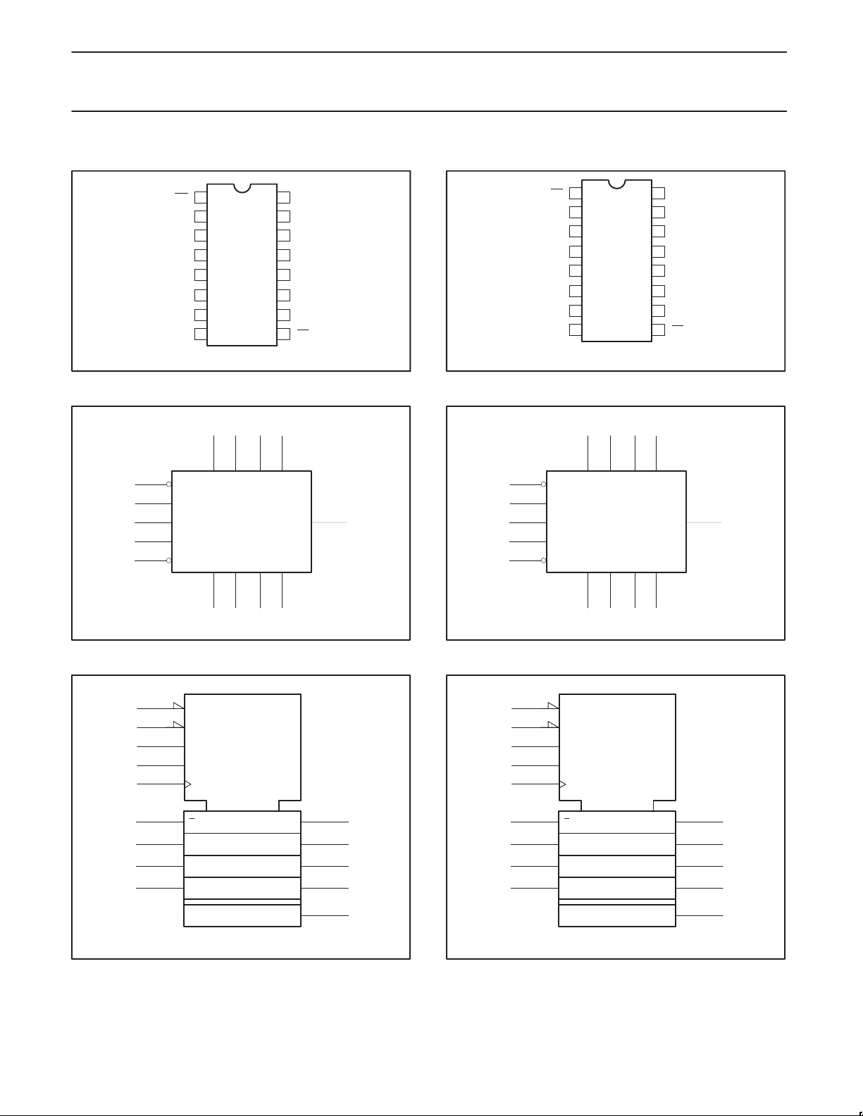
74F161A PIN CONFIGURA TION
MR
1
CP
2
D0
3
D1
4
D2
5
D3
6
CEP
74F161A LOGIC SYMBOL
34
9
7
10
2
1MR
PE
CEP
CET
CP
Q0 Q1
56
D1 D2
Q2 Q3
16
V
CC
TC
15
Q0
14
Q1
13
Q2
12
Q3
11
CET
107
98GND PE
SF00656
D3D0
TC 15
74F163A PIN CONFIGURA TION
SR
1
CP
2
D0
3
D1
4
D2
5
D3
6
CEP
74F163A LOGIC SYMBOL
34
9
7
10
2
1SR
PE
CEP
CET
CP
Q0 Q1
56
D1 D2
Q2 Q3
16
V
CC
TC
15
Q0
14
Q1
13
Q2
12
Q3
11
CET
107
98GND PE
SF00657
D3D0
TC 15
= Pin 16
CC
GND = Pin 8
14 13
12 11V
74F161A LOGIC SYMBOL (IEEE/IEC)
1
9
7
10
2
3
4
5
6
R
M1
G3
G4
C2 /1,3,4+
,2 D
1
CTR DIV 16
4 CT=15
SF00658
SF00660
= Pin 16
CC
GND = Pin 8
14 13
12 11V
SF00659
74F163A LOGIC SYMBOL (IEEE/IEC)
1
9
7
10
2
14
13
12
11
15
3
4
5
6
2R
M1
G3
G4
C2 /1,3,4+
,2 D
1
CTR DIV 16
4 CT=15
14
13
12
11
15
SF00661
1996 Jan 29
3
Page 4

Philips Semiconductors Product specification
OPERATING MODE
Parallel load
Hold (do nothing)
74F161A, 74F163A4-bit binary counters
STATE DIAGRAM
0 1 2 3
15
14
13
12 11 10 9
H H = Enable count
or
L L = Disable count
PE
CEP
CET
CP
SR
Q0 Q1 Q2 Q3
APPLICATIONS
+V
CC
4
D1 D2
5
6
7
8
CLOCK
PE
CEP
CET
CP
SR
Q0 Q1 Q2 Q3
Figure 1. Maximum count modifying scheme
Terminal count = 6
SF00664
D1 D2 D3D0
TC74F163A
PE
CEP
CET
CP
SR
Q0 Q1 Q2 Q3
D1 D2 D3D0
TC74F163A
PE
CEP
CET
CP
SR
Q0 Q1 Q2 Q3
D1 D2 D3D0
TC74F163A
PE
CEP
CET
CP
SR
Q0 Q1 Q2 Q3
D1 D2 D3D0
TC74F163A
D3D0
TC74F163A
SF00665
PE
CEP
CET
CP
SR
Q0 Q1 Q2 Q3
D1 D2
D3D0
TC74F163A
CP
Figure 2. Synchronous multistage counting scheme
74F161A MODE SELECT – FUNCTION TABLE
INPUTS OUTPUTS
MR CP CEP CET PE Dn Qn TC
L X X X X X L L Reset (clear)
H ↑ X X l l L L
H ↑ X X l h H (1)
H ↑ h h h X count (1) Count
H X l X h X q
H X X l h X q
n
n
(1)
L
SF00666
1996 Jan 29
4
Page 5

Philips Semiconductors Product specification
OPERATING MODE
Parallel load
Hold (do nothing)
74F161A, 74F163A4-bit binary counters
74F163A MODE SELECT – FUNCTION TABLE
INPUTS OUTPUTS
SR CP CEP CET PE Dn Qn TC
l ↑ X X X X L L Reset (clear)
h ↑ X X l l L L
h ↑ X X l h H (2)
h ↑ h h h X count (2) Count
h X l X h X q
h X X l h X q
n
n
H = High voltage level
h = High voltage level one setup prior to the Low-to-High clock transition
L = Low voltage level
l = Low voltage level one setup prior to the Low-to-High clock transition
= Lower case letters indicate the state of the referenced output prior to the Low-to-High clock transition
q
n
X = Don’t care
↑ = Low-to-High clock transition
(1) = The TC output is High when CET is High and the counter is at Terminal Count (HHHH for 74F161A)
(2) = The TC output is High when CET is High and the counter is at Terminal Count (HHHH for 74F163A)
(2)
L
74F161A LOGIC DIAGRAM
2
CP
1
MR
9
PE
10
CET
7
CEP
3
D0
4
D1
5
D2
R
DCPQ
R
DCPQ
R
DCPQ
14
Q
Q
Q
Q0
13
Q1
12
Q2
VCC = Pin 16
GND = Pin 8
1996 Jan 29
6
D3
R
DCPQ
11
15
SF00662
Q3
TC
Q
5
Page 6

Philips Semiconductors Product specification
T
Operating free-air temperature range
74F161A, 74F163A4-bit binary counters
74F163A LOGIC DIAGRAM
2
CP
1
SR
9
PE
10
CET
7
CEP
3
D0
DCPQ
14
Q
4
D1
DCPQ
Q0
5
D2
6
D3
VCC = Pin 16
GND = Pin 8
ABSOLUTE MAXIMUM RATINGS
(Operation beyond the limits set forth in this table may impair the useful life of the device.
Unless otherwise noted these limits are over the operating free-air temperature range.)
SYMBOL
V
CC
V
IN
I
IN
V
OUT
I
OUT
amb
T
stg
Supply voltage –0.5 to +7.0 V
Input voltage –0.5 to +7.0 V
Input current –30 to +5 mA
Voltage applied to output in High output state –0.5 to V
Current applied to output in Low output state 40 mA
p
p
Storage temperature range –65 to +150 °C
PARAMETER RATING UNIT
Commercial range 0 to +70 °C
Industrial range –40 to +85 °C
DCPQ
DCPQ
13
12
11
15
SF00663
Q1
Q2
Q3
TC
V
Q
Q
Q
CC
1996 Jan 29
6
Page 7

Philips Semiconductors Product specification
SYMBOL
PARAMETER
UNIT
T
Operating free-air temperature range
SYMBOL
PARAMETER
TEST CONDITIONS
1
UNIT
VOHHigh-level output voltage
CC
,
IL
,
I
MAX
VOLLow-level output voltage
CC
,
IL
,
I
MAX
IILLow-level input current
V
MAX, V
5V
ICCSupply current (total)
V
MAX
74F161A, 74F163A4-bit binary counters
RECOMMENDED OPERATING CONDITIONS
LIMITS
MIN NOM MAX
V
CC
V
IH
V
IL
I
IK
I
OH
I
OL
amb
DC ELECTRICAL CHARACTERISTICS
(Over recommended operating free-air temperature range unless otherwise noted.)
V
IK
I
I
I
IH
I
OS
NOTES:
1. For conditions shown as MIN or MAX, use the appropriate value specified under recommended operating conditions for the applicable type.
2. All typical values are at V
3. Not more than one output should be shorted at a time. For testing I
techniques are preferable in order to minimize internal heating and more accurately reflect operational values. Otherwise, prolonged shorting
of a High output may raise the chip temperature well above normal and thereby cause invalid readings in other parameter tests. In any
sequence of parameter tests, I
Supply voltage 4.5 5.0 5.5 V
High-level input voltage 2.0 V
Low-level input voltage 0.8 V
Input clamp current –18 mA
High-level output current –1 mA
Low-level output current 20 mA
p
p
Commercial range 0 +70 °C
Industrial range –40 +85 °C
LIMITS
MIN TYP2MAX
p
p
VCC = MIN, VIL = MAX,
VIH = MIN
VCC = MIN, VIL = MAX,
VIH = MIN
Input clamp voltage VCC = MIN, II = I
=
OH
=
OL
IK
±10%V
±5%V
±10%V
±5%V
2.5 V
CC
2.7 3.4 V
CC
CC
CC
0.30 0.50 V
0.30 0.50 V
–0.73 –1.2 V
Input current at maximum input voltage VCC = MAX, VI = 7.0V 100 µA
High-level input current VCC = MAX, VI = 2.7V 20 µA
p
Short-circuit output current
pp
= 5V, T
CC
amb
tests should be performed last.
OS
CET, PE
3
= 25°C.
others
I
CCH
I
CCL
CC
=
= 0.
I
VCC = MAX -60 –150 mA
=
CC
, the use of high-speed test apparatus and/or sample-and-hold
OS
–1.2 mA
–0.6 mA
42 55 mA
49 65 mA
1996 Jan 29
7
Page 8

Philips Semiconductors Product specification
74F161A, 74F163A4-bit binary counters
AC ELECTRICAL CHARACTERISTICS
LIMITS
T
SYMBOL PARAMETER
f
t
t
t
t
t
t
t
t
t
t
max
PLH
PHL
PLH
PHL
PLH
PHL
PLH
PHL
PHL
PHL
Maximum clock frequency Waveform 1 100 130 90 75 MHz
Propagation delay
CP to Qn (PE = High)
Propagation delay
CP to Qn (PE = Low)
Propagation delay
CP to TC
Propagation delay
CET to TC
Propagation delay
MR to Qn
Propagation delay
MR to TC
= +25°C
amb
TEST
CONDITION
VCC = +5.0V
C
= 50pF
L
R
= 500Ω
L
MIN TYP MAX MIN MAX MIN MAX
2.0
Waveform 1
Waveform 1
Waveform 1
Waveform 2
4.0
2.0
3.5
5.0
4.5
1.5
2.5
4.0
6.5
4.5
5.5
7.5
7.5
3.5
5.0
’F161A Waveform 3 6.0 8.5 12.0 5.5 13.0 5.5 13.0 ns
’F161A Waveform 3 5.0 8.5 10.0 5.0 11.0 5.0 11.0 ns
T
amb
VCC = +5.0V ± 10%
6.5
10.0
6.5
8.5
10.5
10.5
6.5
7.5
= 0°C to +70°C
C
= 50pF
L
R
= 500Ω
L
2.0
4.0
11.0
2.0
3.5
5.0
4.0
11.5
11.5
1.5
2.5
7.0
7.5
9.5
7.0
8.0
T
= –40°C to +85°C
amb
VCC = +5.0V ± 10%
C
= 50pF
L
R
= 500Ω
L
2.0
4.0
2.0
3.5
5.0
4.0
1.5
2.5
7.0
11.0
7.5
9.5
11.5
11.5
7.0
8.0
UNIT
ns
ns
ns
ns
AC SETUP REQUIREMENTS
SYMBOL PARAMETER
ts(H)
ts(L)
th(H)
th(L)
ts(H)
ts(L)
th(H)
th(L)
ts(H)
ts(L)
th(H)
th(L)
tw(H)
tw(L)
tw(H)
tw(L)
tw(L)
t
REC
Setup time, High or Low
Dn to CP
Hold time, High or Low
Dn to CP
Setup time, High or Low
PE or SR to CP
Hold time, High or Low
PE or SR to CP
Setup time, High or Low
CET or CEP to CP
Hold time, High or Low
CET or CEP to CP
CP pulse width (Load)
High or Low
CP pulse width (Count)
High or Low
MR pulse width
Low
Recovery time
MR to CP
’F161A Waveform 3 4.5 4.5 4.5 ns
’F161A Waveform 3 6.0 6.5 6.5 ns
TEST
CONDITION
Waveform 6
Waveform 6
Waveform
5 or 6
Waveform
5 or 6
Waveform 4
Waveform 4
Waveform 1
Waveform 1
LIMITS
T
= +25°C
amb
VCC = +5.0V
C
= 50pF
L
R
= 500Ω
L
T
= 0°C to +70°C
amb
VCC = +5.0V ± 10%
C
= 50pF
L
R
= 500Ω
L
T
= –40°C to +85°C
amb
VCC = +5.0V ± 10%
C
= 50pF
L
R
= 500Ω
L
MIN TYP MIN MIN
5.0
5.0
0
0
9.0
6.5
0
0
10.5
6.0
0
0
4.0
5.0
4.0
6.0
5.0
5.0
0
0
9.5
7.0
0
0
10.5
7.0
0
0
4.0
5.5
4.0
7.0
5.0
5.0
0
0
9.5
7.0
0
0
10.5
7.0
0
0
4.0
7.0
4.0
7.0
UNIT
ns
ns
ns
ns
ns
ns
ns
ns
1996 Jan 29
8
Page 9

Philips Semiconductors Product specification
74F161A, 74F163A4-bit binary counters
AC WAVEFORMS
For all waveforms, VM = 1.5V.
The shaded areas indicate when the input is permitted to change for predictable output performance.
1/f
MAX
CP
Qn, TC
V
M
tw(H) tw(L)
t
PLH
V
M
V
M
V
M
t
PHL
V
M
SF00667
Waveform 1. Propagation Delay, Clock Input to Output,
Clock Pulse Width, and Maximum Clock Frequency
tw(L)
MR
CP
Qn, TC
V
M
t
PHL
V
M
t
REC
V
M
V
M
SF00669
Waveform 3. Master Reset Pulse Width, Master Reset to
Output Delay, and Master Reset to Recovery T ime
CET
TC
V
M
t
PLH
V
M
V
M
t
PHL
V
M
SF00668
Waveform 2. Propagation Delay, CET Input to TC Output
CEP
CET
CP
V
V
M
M
ts(H) ts(L)th(H) th(L)
V
M
V
MVM
V
M
SF00670
Waveform 4. CEP and CET Reset Setup and Hold Times
SR
CP
V
V
M
M
ts(L) ts(H)th(L) th(H)
V
M
V
V
M
M
Waveform 5. Synchronous Reset Setup and Hold Times
1996 Jan 29
V
M
SF00671
V
V
M
M
t
t
s
h
V
M
V
M
V
MVM
V
M
PE
CP
Dn
V
M
ts(L) ts(H)th(L) th(H)
SF00672
Waveform 6. Parallel Data and Parallel Enable
Setup and Hold Times
9
Page 10

Philips Semiconductors Product specification
74F161A, 74F163A4-bit binary counters
TEST CIRCUIT AND WAVEFORMS
V
CC
PULSE
GENERATOR
V
IN
R
T
D.U.T.
V
OUT
R
C
L
L
Test Circuit for Totem-Pole Outputs
DEFINITIONS:
= Load resistor;
R
L
see AC ELECTRICAL CHARACTERISTICS for value.
= Load capacitance includes jig and probe capacitance;
C
L
see AC ELECTRICAL CHARACTERISTICS for value.
R
= T ermination resistance should be equal to Z
T
pulse generators.
OUT
of
NEGATIVE
PULSE
POSITIVE
PULSE
family
74F
90%
10%
amplitude
3.0V
t
w
V
M
10%
)
V
90%
M
t
THL (tf
t
TLH (tr
)
t
t
t
w
TLH (tr
THL (tf
10%
)
)
90%
V
M
V
Input Pulse Definition
INPUT PULSE REQUIREMENTS
V
M
1.5V
rep. rate
1MHz 500ns
t
w
90%
M
10%
t
TLHtTHL
2.5ns 2.5ns
AMP (V)
0V
AMP (V)
0V
SF00006
1996 Jan 29
10
Page 11

Philips Semiconductors Product specification
4-bit binary counters
DIP16: plastic dual in-line package; 16 leads (300 mil) SOT38-4
74F162A
*, 74F163A
74F160A*, 74F161A,
* Discontinued part. Please see the Discontinued Product List in Section 1, page 21.
1996 Jan 29
11
Page 12

Philips Semiconductors Product specification
4-bit binary counters
SO16: plastic small outline package; 16 leads; body width 3.9 mm SOT109-1
74F162A
*, 74F163A
74F160A*, 74F161A,
* Discontinued part. Please see the Discontinued Product List in Section 1, page 21.
1996 Jan 29
12
Page 13

Philips Semiconductors Product specification
4-bit binary counters
NOTES
74F160A*, 74F161A,
74F162A
*, 74F163A
* Discontinued part. Please see the Discontinued Product List in Section 1, page 21.
1996 Jan 29
13
Page 14

Philips Semiconductors Product specification
4-bit binary counter
Data sheet status
Data sheet
status
Objective
specification
Preliminary
specification
Product
specification
Product
status
Development
Qualification
Production
74F160A*, 74F161A,
74F162A*, 74F163A
Definition
This data sheet contains the design target or goal specifications for product development.
Specification may change in any manner without notice.
This data sheet contains preliminary data, and supplementary data will be published at a later date.
Philips Semiconductors reserves the right to make chages at any time without notice in order to
improve design and supply the best possible product.
This data sheet contains final specifications. Philips Semiconductors reserves the right to make
changes at any time without notice in order to improve design and supply the best possible product.
[1]
[1] Please consult the most recently issued datasheet before initiating or completing a design.
Definitions
Short-form specification — The data in a short-form specification is extracted from a full data sheet with the same type number and title. For
detailed information see the relevant data sheet or data handbook.
Limiting values definition — Limiting values given are in accordance with the Absolute Maximum Rating System (IEC 134). Stress above one
or more of the limiting values may cause permanent damage to the device. These are stress ratings only and operation of the device at these or
at any other conditions above those given in the Characteristics sections of the specification is not implied. Exposure to limiting values for extended
periods may affect device reliability.
Application information — Applications that are described herein for any of these products are for illustrative purposes only. Philips
Semiconductors make no representation or warranty that such applications will be suitable for the specified use without further testing or
modification.
Disclaimers
Life support — These products are not designed for use in life support appliances, devices or systems where malfunction of these products can
reasonably be expected to result in personal injury . Philips Semiconductors customers using or selling these products for use in such applications
do so at their own risk and agree to fully indemnify Philips Semiconductors for any damages resulting from such application.
Right to make changes — Philips Semiconductors reserves the right to make changes, without notice, in the products, including circuits, standard
cells, and/or software, described or contained herein in order to improve design and/or performance. Philips Semiconductors assumes no
responsibility or liability for the use of any of these products, conveys no license or title under any patent, copyright, or mask work right to these
products, and makes no representations or warranties that these products are free from patent, copyright, or mask work right infringement, unless
otherwise specified.
Philips Semiconductors
811 East Arques Avenue
P.O. Box 3409
Sunnyvale, California 94088–3409
Telephone 800-234-7381
* Discontinued part. Please see the Discontinued Product List in Section 1, page 21.
Copyright Philips Electronics North America Corporation 1998
All rights reserved. Printed in U.S.A.
print code Date of release: 10-98
Document order number: 9397-750-05084
yyyy mmm dd
14
 Loading...