

Page 1
查询74F161A供应商
74F161A • 74F163A
Synchronous Presettable Binary Counter
74F161A • 74F163A Synchronous Presettable Binary Counter
April 1988
Revised July 1999
General Description
The 74F161A and 74F 163A are high-speed synchr onous
modulo-16 binary counte rs. They are synchronously presettable for application in progr ammab le divide rs and have
two types of Count Enable input s plus a Terminal Count
output for versatility in forming synchronous multi-stage
counters. The 74F161A has an asynchronous MasterReset input that overr ides all other inputs and f orces the
outputs LOW. The 74F163A has a Synchronous Reset
input that overrides counting and parallel loading and
allows the outputs to be sim ultaneously reset on the r ising
edge of the clock. The 74 F161A and 74F163A are hig hspeed versions of the 74F161 and 74F163.
Features
■ Synchronous counting and loading
■ High-speed synchronous expan si on
■ Typical count frequency of 120 MHz
Ordering Code:
Order Number Package Number Package Description
74F161ASC M16A 16-Lead Small Outline Integrated Circuit (SOIC), JEDEC MS-012, 0.150 Narrow
74F161ASJ M16D 16-Lead Small Outline Package (SOP), EIAJ TYPE II, 5.3mm Wide
74F161APC N16E 16-Lead Plastic Dual-In-Line Package (PDIP), JEDEC MS-001, 0.300 Wide
74F163ASC M16A 16-Lead Small Outline Integrated Circuit (SOIC), JEDEC MS-012, 0.150 Narrow
74F163ASJ M16D 16-Lead Small Outline Package (SOP), EIAJ TYPE II, 5.3mm Wide
74F163APC N16E 16-Lead Plastic Dual-In-Line Package (PDIP), JEDEC MS-001, 0.300 Wide
Devices also availab le in Tape and Reel. Specify by appending th e s uffix let t er “X” to the ordering cod e.
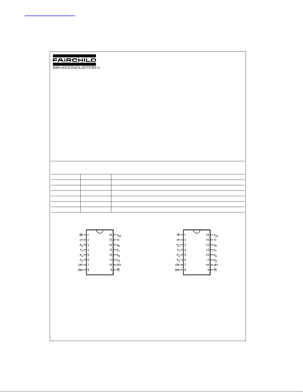
Connection Diagrams
74F161A 74F163A
© 1999 Fairchild Semiconductor Corporation DS009486 www.fairchildsemi.com
Page 2
Logic Symbols
74F161A • 74F163A
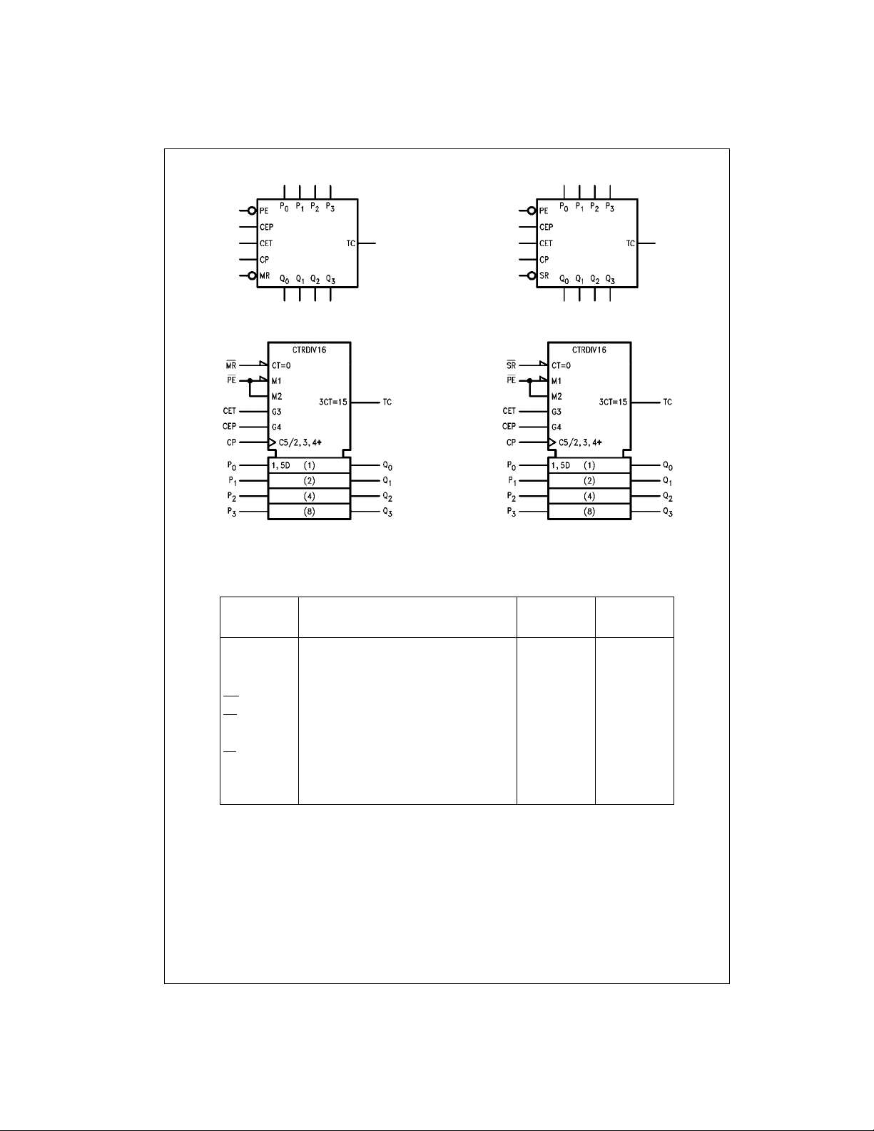
74F161A
IEEE/IEC
74F163A
IEEE/IEC
74F161A
Unit Loading/Fan Out
Pin Names Description
CEP Count Enable Parallel Input 1.0/1.0 20 µA/−0.6 mA
CET Count Enable Trickle Input 1.0/2.0 20 µA/−1.2 mA
CP Clock Pulse Input (Active Rising Edge) 1.0/1.0 20 µA/−0.6 mA
(74F161A) Asynchronous Master Reset Input (Active LOW) 1.0/1.0 20 µA/−0.6 mA
MR
(74F163A) Synchronous Reset Input (Active LOW) 1.0/2.0 20 µA/−1.2 mA
SR
P
0–P3
PE
Q
0–Q3
TC Terminal Count Output 50/33.3 −1 mA/20 mA
Parallel Data Inputs 1.0/1.0 20 µA/−0.6 mA
Parallel Enable Input (Active LOW) 1.0/2.0 20 µA/−1.2 mA
Flip-Flop Outputs 50/33.3 −1 mA/20 mA
74F163A
U.L.
HIGH/LOW
Input I
Output I
IH/IIL
OH/IOL
www.fairchildsemi.com 2
Page 3
Functional Description
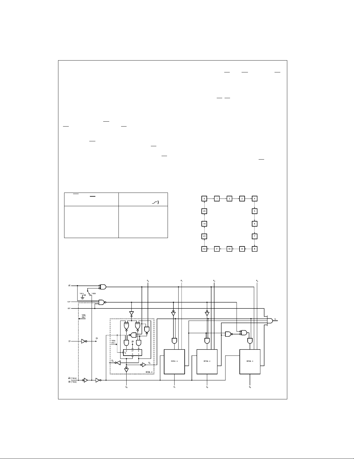
The 74F161A and 74F163A count in modulo-16 binary
sequence. From state 15 (HHHH) they increment to state 0
(LLLL). The clock inputs of all flip-flops are driven in parallel through a clock buffer. Thus all changes of the Q outputs
(except due to Master Rese t of the 74F161A) occur as a
result of, and synchron ous with, the LOW-to-H IGH transition of the CP inpu t signal. The circuits hav e four fundamental modes of operation, in order of precedence:
asynchronous reset (74F161A), synchronous reset
(74F163A), parallel load, count-up and hold. Five control
inputs—Master Reset (MR
, 74F163A), Parallel Enable (PE), Count Enable Paral-
(SR
lel (CEP) and Count Enable Trickle (CET)—determine the
mode of operation, as show n in the Mode Select Table. A
LOW signal on MR
nously forces all out puts LOW. A LOW sign al on SR
rides counting and parallel loading and allows all outputs to
go LOW on the next rising edge of CP. A LOW signal on PE
overrides counting an d allows information on the Parallel
) inputs to be loaded i nto t he flip -flops o n the n ext
Data (P
n
, 74F161A), Synchronous Reset
overrides all other inputs and asynchro-
over-
rising edge of CP. With PE
(74F163A) HIGH, CEP and CET permit counting when
both are HIGH. Conversely, a LOW signal on either CEP or
CET inhibits counting.
The 74F161A and 74F163A use D-type edge triggered flipflops and changing the SR
the CP is in either state does not cause errors, pro vided
that the recommended set up and hold times, wit h respect
to the rising edge of CP, are observed.
The Terminal Count (TC) output is HIGH when CET is
HIGH and th e c o un t er is i n s ta te 15 . To impl em en t sy n chr o nous multi-stage counters, the TC outputs can be used
with the CEP and CET in pu ts in t w o d ifferent w ays. Please
refer to the 74F568 data sheet. The TC output is subject to
decoding spikes due to internal race conditions and is
therefore not recommended for use as a clock or asynchronous reset for flip-flops, counters or registers.
Logic Equations: Count Enable = CEP • CET • PE
and MR ('F161A) or SR
, PE, CEP and CET inputs when
TC = Q0 • Q1 • Q2 • Q3 • CET
74F161A • 74F163A
Mode Select Table
SR
(Note 1)
H = HIGH Voltage Level
L = LOW Voltage Level
X = Immaterial
Note 1: For 74F163A only
PE
L X X X Reset (Clear)
H L X X Load (P
H H H H Count (Increment)
H H L X No Change (Hold)
H H X L No Change (Hold)
CET
CE
P
Block Diagram
Action on the Rising
Clock Edge (
n→Qn
)
)
State Diagram
3 www.fairchildsemi.com
Page 4
Absolute Maximum Ratings(Note 2) Recommended Operating
Storage Temperature −65°C to +150°C
Ambient Temperature under Bias −55°C to +125°C
Junction Temperature under Bias −55°C to +150°C
Pin Potential to Ground Pin −0.5V to +7.0V
V
CC
Input Voltage (Note 3) −0.5V to +7.0V
Input Current (Note 3) −30 mA to +5.0 mA
Voltage Applied to Output
74F161A • 74F163A
in HIGH State (with V
CC
= 0V)
Standard Output −0.5V to V
3-STATE Output −0.5V to +5.5V
Current Applied to Output
in LOW State (Max) twice the rated I
ESD Last Passing Voltage (Min) 4000V
OL
Conditions
Free Air Ambient Temperature 0°C to +70°C
Supply Voltage +4.5V to +5.5V
Note 2: Absolute maximum ratings are values beyond which the device
CC
may be damaged or have its useful life impaired. Functional operation
under these conditi ons is not implied.
Note 3: Either voltage limit or curren t limit is sufficient to protect in put s .
(mA)
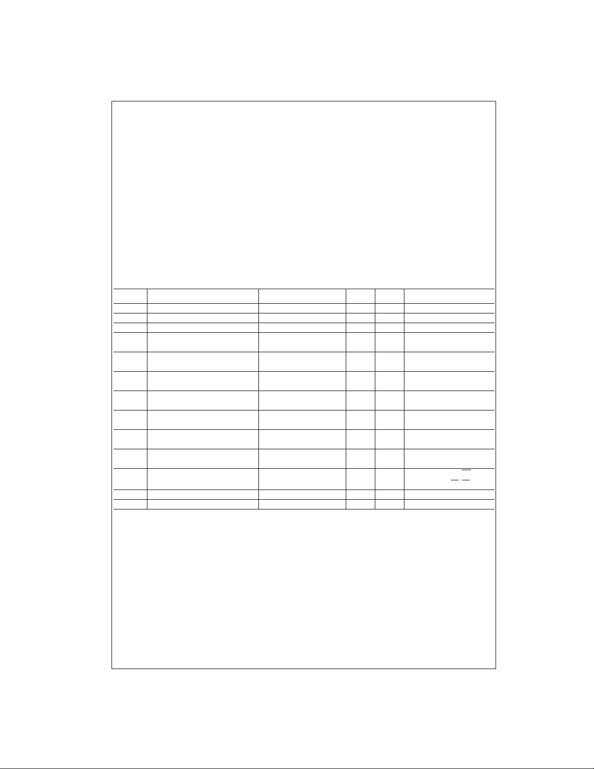
DC Electrical Characteristics
Symbol Parameter Min Typ Max Units
V
V
V
V
V
I
I
I
V
I
I
I
I
IH
IL
CD
OH
OL
IH
BVI
CEX
ID
OD
IL
OS
CC
Input HIGH Voltage 2.0 V Recognized as a HIGH Signal
Input LOW Voltage 0.8 V Recognized as a LOW Signal
Input Clamp Diode Voltage −1.2 V Min IIN = −18 mA
Output HIGH 10% V
Voltage 5% V
Output LOW 10% V
Voltage
Input HIGH
Current
Input HIGH Current
Breakdown Test
Output HIGH
Leakage Current
Input Leakage
Test All Other Pins Grounded
Output Leakage
Circuit Current All Other Pins Grounded
Input LOW Current −0.6 mA Max VIN = 0.5V (CEP, CP, MR, P0–P3)
Output Short-Circuit Current −60 −150 mA Max V
Power Supply Current 37 55 mA Max
2.5
CC
2.7
CC
CC
4.75 V 0.0
0.5 V Min IOL = 20 mA
5.0 µAMaxVIN = 2.7V
7.0 µAMaxVIN = 7.0V
50 µAMaxV
3.75 µA0.0
−1.2 mA Max
V
CC
VMin
IID = 1.9 µA
V
VIN = 0.5V (CET, PE, SR)
= V
OUT
= 150 mV
IOD
= 0V
OUT
Conditions
CC
www.fairchildsemi.com 4
Page 5
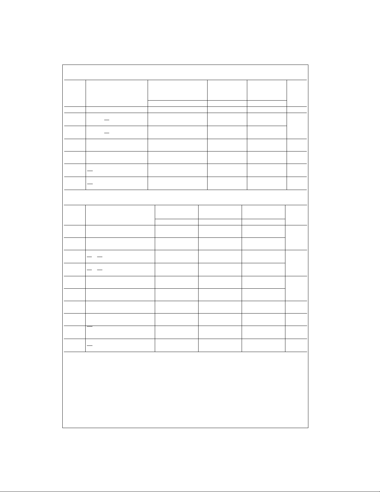
AC Electrical Characteristics
Symbol Parameter
f
t
t
t
t
t
t
t
t
t
MAX
PLH
PHL
PLH
PHL
PLH
PHL
PLH
PHL
PHL
Maximum Count Frequency 100 120 75 90 MHz
Propagation Delay 3.5 5.5 7.5 3.5 9.0 3.5 8.5
CP to Qn (PE Input HIGH)
Propagation Delay 4.0 6.0 8.5 4.0 10.0 4.0 9.5
CP to Qn (PE Input LOW)
Propagation Delay 5.0 10.0 14.0 5.0 16.5 5.0 15.0
CP to TC 5.0 10.0 14.0 5.0 15.5 5.0 15.0
Propagation Delay 2.5 4.5 7.5 2.5 9.0 2.5 8.5
CET to TC 2.5 4.5 7.5 2.5 9.0 2.5 8.5
Propagation Delay 5.5 9.0 12.0 5.5 14.0 5.5 13.0 ns
MR to Qn (74F161A)
t
PHL
Propagation Delay 4.5 8.0 10.5 4.5 12.5 4.5 11.5 ns
MR to TC (74F161A)
TA = +25°CT
VCC = +5.0V VCC = +5.0V VCC = +5.0V
CL = 50 pF CL = 50 pF CL = 50 pF
Min Typ Max Min Max Min Max
3.5 7.5 10.0 3.5 11.5 3.5 11.0
4.0 6.0 8.5 4.0 10.0 4.0 9.5
= −55°C to +125°CTA = 0°C to +70°C
A
Units
AC Operating Requirements
TA = +25°CT
Symbol Parameter
Min Max Min Max Min Max
tS(H) Setup Time, HIGH or LOW 5.0 5.5 5.0
tS(L) Pn to CP 5.0 5.5 5.0
tH(H) Hold Time, HIGH or LOW 2.0 2.5 2.0
tH(L) Pn to CP 2.0 2.5 2.0
tS(H) Setup Time, HIGH or LOW 11.0 13.5 11.5
tS(L)
PE or SR to CP
8.510.59.5
tH(H) Hold Time, HIGH or LOW 2.0 3.6 2.0
tH(L)
PE or SR to CP
000
tS(H) Setup Time, HIGH or LOW 11.0 13.0 11.5
tS(L) CEP or CET to CP 5.0 6.0 5.0
tH(H) Hold Time, HIGH or LOW 0 0 0
tH(L) CEP or CET to CP 0 0 0
tW(H) Clock Pulse Width (Load) 5.0 5.0 5.0
tW(L) HIGH or LOW 5.0 5.0 5.0
tW(H) Clock Pulse Width (Count) 4.0 5.0 4.0
tW(L) HIGH or LOW 6.0 8.0 7.0
tW(L) MR Pulse Width, LOW 5.0 5.0 5.0 ns
(74F161A)
t
REC
Recovery Time 6.0 6.0 6.0 ns
MR to CP (74F161A)
= −55°C to +125°CTA = 0°C to +70°C
A
UnitsVCC = +5.0V VCC = +5.0V VCC = +5.0V
74F161A • 74F163A
ns
ns
ns
ns
ns
ns
ns
ns
5 www.fairchildsemi.com
Page 6
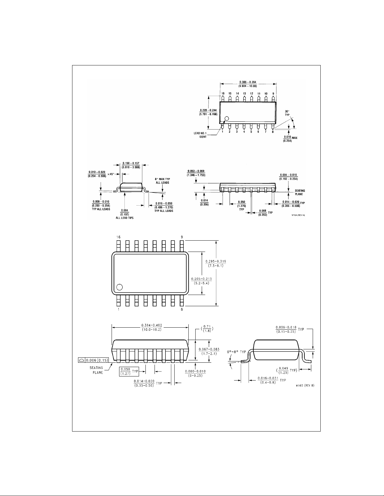
Physical Dimensions inches (millimeters) unless otherwise noted
74F161A • 74F163A
16-Lead Small Outline Integrated Circuit (SOIC), JEDEC MS-012, 0.150 Narrow
16-Lead Small Outline Package ( SOP), EIAJ TYPE II, 5.3mm Wide
Package Number M16A
Package Number M16D
www.fairchildsemi.com 6
Page 7
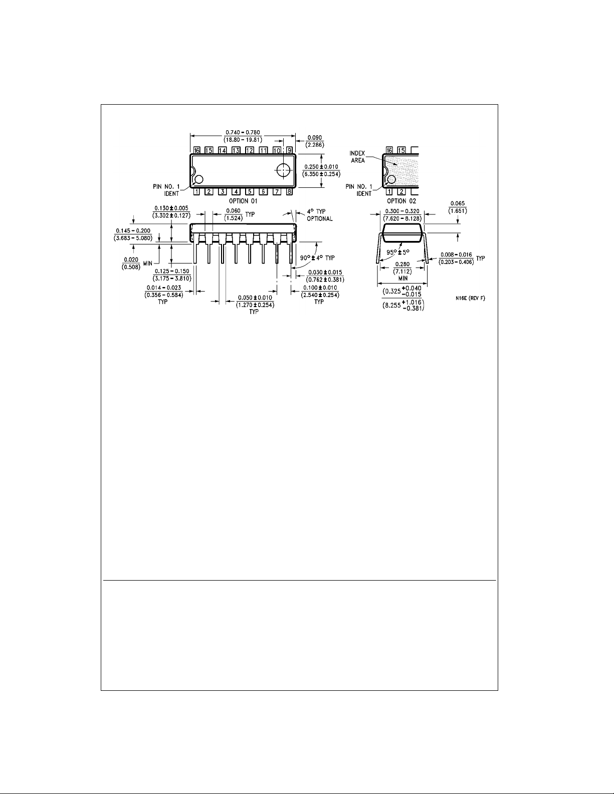
Physical Dimensions inches (millimeters) unless otherwise noted (Continued)
74F161A • 74F163A Synchronous Presettable Binary Counter
16-Lead Plastic Dual-In-Line Package (PDIP), JEDEC MS-001, 0.300 Wide
Fairchild does not assume any responsibility for use of any circuitry described, no circuit patent license s are implied and
Fairchild reserves the right at any time without notice to change said circuitry and specifications.
LIFE SUPPORT POLICY
FAIRCHILD’S PRODUCTS ARE NOT AUTHORIZED FOR USE AS CRITICAL COMPONENTS IN LIFE SUPPORT
DEVICES OR SYSTEMS WITHOUT THE EXPRESS WRITTEN APPROVAL OF THE PRESIDENT OF FAIRCHILD
SEMICONDUCTOR CORPORATION. As used herein:
1. Life support devices or systems are devices or systems
which, (a) are intended for surgical implant into the
body, or (b) support or sustain life, and (c) whose failure
to perform when properly used in accordance with
instructions for use provide d in the labe l ing, can be re asonably expected to result in a significant injury to the
user.
Package Number N16E
2. A critical componen t in any com ponen t of a life s upport
device or system whose failu re to perform can b e reasonably expected to cause the failure of the life support
device or system, or to affect its safety or effectiveness.
www.fairchildsemi.com
7 www.fairchildsemi.com
 Loading...