

Datasheet 74F153SJX, 74F153SJ, 74F153SCX, 74F153SC, 74F153PC Datasheet (Fairchild Semiconductor)
Page 1
© 1999 Fairchild Semiconductor Corporation DS009482 www.fairchildsemi.com
April 1988
Revised July 1999
74F153 Dual 4-Input Multiplexer
74F153
Dual 4-Input Multiplexer
General Description
The F153 is a high-speed dual 4-input multiplexer with
common select inputs and individual enable inputs for each
section. It can select two lines of data fro m four sources.
The two buffered outputs present data in the true (noninverted) form. In addition to multiplexer operation, the
F153 can generate any two functions of three variables.
Ordering Code:
Devices also availab le in Tape and Reel. Specify by appending th e s uffix let t er “X” to the ordering code.
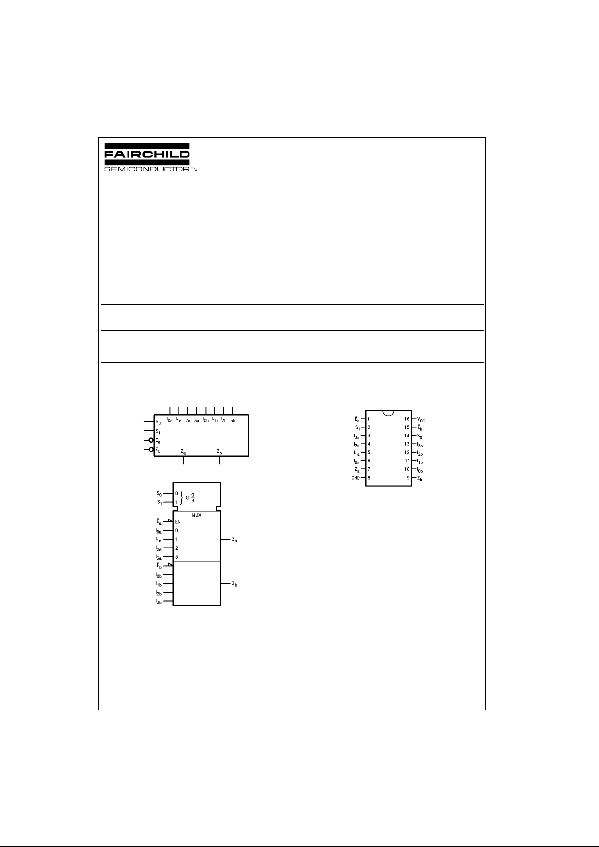
Logic Symbols
IEEE/IEC
Connection Diagram
Order Number Package Number Package Description
74F153SC M16A 16-Lead Small Outline Integrated Circuit (SOIC), JEDEC MS-012, 0.150 Narrow
74F153SJ M16D 16-Lead Small Outline Package (SOP), EIAJ TYPE II, 5.3mm Wide
74F153PC N16E 16-Lead Plastic Dual-In-Line Package (PDIP), JEDEC MS-001, 0.300 Wide
Page 2
www.fairchildsemi.com 2
74F153
Unit Loading/Fan Out
Truth Table
H = HIGH Voltage Level
L = LOW
X = Immaterial
Functional Description
The F153 is a d ua l 4- in pu t mu ltiplexer. It can se l ect t wo b i t s
of data from up to four so urces under the control of the
common Select inputs (S
0
, S1). The two 4-input multiplexer
circuits have individual active LOW Enables (E
a
, Eb) which
can be used to strobe the outputs independently. When the
Enables (E
a
, Eb) are HIGH, the corresponding outputs (Za,
Z
b
) are forced LOW. The F153 is the logic impleme ntation
of a 2-pole, 4-position switch, where the position of the
switch is determined by the logic levels s upplied to the two
Select inputs. The logic e quations for the outputs are as
follows:
Z
a
= Ea•(I0a•S1•S0 + I1a•S1•S0 +
I
2a•S1•S0
+ I3a•S1•S0)
Z
b
= Eb•(I0b•S1•S0 + I1b•S1•S0 +
I
2b•S1•S0
+ I3b•S1•S0)
The F153 can be used to mo ve da ta fr om a gro up of registers to a common output bus. The particular reg ister from
which the data came would be det ermined by the state of
the Select inputs. A less obvious appl ication is as a function generator. The F153 can generate two functions of
three variables. This is useful for implementing highly irregular random logic.
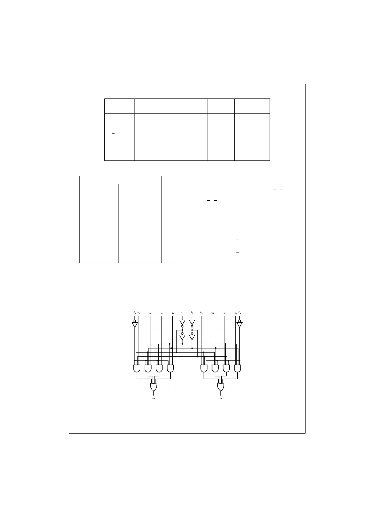
Logic Diagram
Please note that this diagram is provided o nly f or t he understanding of lo gic operations and should not be used to estimate propagation delays.
Pin Names Description
U.L.
Input I
IH/IIL
HIGH/LOW
Output I
OH/IOL
I0a–I
3a
Side A Data Inputs 1.0/1.0 20 µA/−0.6 mA
I
0b–I3b
Side B Data Inputs 1.0/1.0 20 µA/−0.6 mA
S
0
, S
1
Common Select Inputs 1.0/1.0 20 µA/−0.6 mA
E
a
Side A Enable Input (Active LOW) 1.0/1.0 20 µA/−0.6 mA
E
b
Side B Enable Input (Active LOW) 1.0/1.0 20 µA/−0.6 mA
Z
a
Side A Output 50/33.3 −1 mA/20 mA
Z
b
Side B Output 50/33.3 −1 mA/20 mA
Select Inputs Inputs (a or b) Output
S
0
S1E I0I1I2I
3
Z
X X HXXXX L
L L LLXXX L
L L LHXXX H
H L LXLXX L
HLLXHXXH
LHLXXLXL
LHLXXHXH
H H LXXXL L
H H LXXXH H
Page 3

3 www.fairchildsemi.com
74F153
Absolute Maximum Ratings(Note 1) Recommended Operating
Conditions
Note 1: Absolute maximum ratings are values beyon d which the device
may be damaged or have its useful life impaired . Functional operation
under these condit ions is not implied.
Note 2: Either voltage limit or curren t limit is sufficient to protect in puts.
DC Electrical Characteristics
AC Electrical Characteristics
Storage Temperature −65°C to +150°C
Ambient Temperature under Bias −55°C to +125°C
Junction Temperature under Bias −55°C to +150°C
V
CC
Pin Potential to Ground Pin −0.5V to +7.0V
Input Voltage (Note 2) −0.5V to +7.0V
Input Current (Note 2) −30 mA to +5.0 mA
Voltage Applied to Output
in HIGH State (with V
CC
= 0V)
Standard Output −0.5V to V
CC
3-STATE Output −0.5V to +5.5V
Current Applied to Output
in LOW State (Max) twice the rated I
OL
(mA)
Free Air Ambient Temperature 0°C to +70°C
Supply Voltage +4.5V to +5.5V
Symbol Parameter Min Typ Max Units
V
CC
Conditions
V
IH
Input HIGH Voltage 2.0 V Recognized as a HIGH Signal
V
IL
Input LOW Voltage 0.8 V Recognized as a LOW Signal
V
CD
Input Clamp Diode Voltage −1.2 V Min IIN = −18 mA
V
OH
Output HIGH Voltage 10% V
CC
2.5
VMin
IOH = −1 mA
5% V
CC
2.7 IOH = −1 mA
V
OL
Output LOW Voltage 10% V
CC
0.5 V Min IOL = 20 mA
I
IH
Input HIGH Current 5.0 µAMaxVIN = 2.7V
I
BVI
Input HIGH Current Breakdown Test 7.0 µAMaxVIN = 7.0V
I
CEX
Output High Leakage Current 50 µAMaxV
OUT
= V
CC
V
ID
Input Leakage Test 4.75 V 0.0 IID = 1.9 µA
All Other Pins Grounded
I
OD
Output Leakage Circuit Current 3.75 µA0.0V
IOD
= 150 mV
All Other Pins Grounded
I
IL
Input LOW Current −0.6 mA Max VIN = 0.5V
I
OS
Output Short-Circuit Current −60 −150 mA Max V
OUT
= 0V
I
CCL
Power Supply Current 12 20 mA Max VO = LOW
Symbol Parameter
TA = +25°CT
A
= 0°C to +70°C
Units
VCC = +5.0V VCC = +5.0V
CL = 50 pF CL = 50 pF
Min Typ Max Min Max
t
PLH
Propagation Delay 4.5 8.1 10.5 4.5 12.0
ns
t
PHL
Sn to Zn 3.5 7.0 9.0 3.5 10.5
t
PLH
Propagation Delay 4.5 7.1 9.0 4.5 10.5
ns
t
PHL
En to Zn
3.05.77.02.58.0
t
PLH
Propagation Delay 3.0 5.3 7.0 3.0 8.0
ns
t
PHL
In to Zn 2.55.16.52.57.5
Page 4

www.fairchildsemi.com 4
74F153
Physical Dimensions inches (millimeters) unless otherwise noted
16-Lead Small Outline Integrated Circuit (SOIC), JEDEC MS-012, 0.150 Narrow
Package Number M16A
16-Lead Small Outline Package (SOP), EIAJ TYPE II, 5.3mm Wide
Package Number M16D
Page 5

5 www.fairchildsemi.com
74F153 Dual 4-Input Multiplexer
Physical Dimensions inches (millimeters) unless otherwise noted (Continued)
16-Lead Plastic Dual-In-Line Package (PDIP), JEDEC MS-001, 0.300 Wide
Package Number N16E
Fairchild does not assume any responsibility for use of any circu itry described, no circuit patent license s are implied and
Fairchild reserves the right at any time without notice to change said circuitry and specifications.
LIFE SUPPORT POLICY
FAIRCHILD’S PRODUCTS ARE NOT AUTHORIZED FOR USE AS CRITICAL COMPONENTS IN LIFE SUPPORT
DEVICES OR SYSTEMS WITHOUT THE EXPRESS WRITTEN APPROVAL OF THE PRESIDENT OF FAIRCHILD
SEMICONDUCTOR CORPORATION. As used herein:
1. Life suppor t de vices o r syst ems are dev ic es or syste ms
which, (a) are intended for surgical implant into the
body, or (b) support or sustain life, and (c) whose failure
to perform when properly used in accordance with
instructions for use provided i n the labe li ng, can be re asonably expected to result in a significant injury to the
user.
2. A criti cal com ponen t in any compo nent o f a li fe supp ort
device or system whose failu re to perform can b e reasonably expected to c ause th e fa i lure of the li fe s upp or t
device or system, or to affect its safety or effectiveness.
www.fairchildsemi.com
 Loading...