

Datasheet 74F138SJX, 74F138SJ, 74F138SCX, 74F138SC, 74F138PC Datasheet (Fairchild Semiconductor)
Page 1
© 1999 Fairchild Semiconductor Corporation DS009478 www.fairchildsemi.com
April 1988
Revised July 1999
74F138 1-of-8 Decoder/Demultiplexer
74F138
1-of-8 Decoder/Demultiplex er
General Description
The F138 is a high-speed 1-of-8 decoder/demultiplexer.
This device is ideally suited for high-speed bipolar memory
chip select address decoding. The multiple input ena bles
allow parallel expans ion to a 1-of-24 dec oder using just
three F138 devices or a 1-of-32 dec oder using fo ur F138
devices and one inverter.
Features
■ Demultiplexing capability
■ Multiple input enable for easy expansion
■ Active LOW mutually exclusive outputs
Ordering Code:
Devices also available in Tape and Reel. Specify by appending the suffix letter “X” to the ordering code.
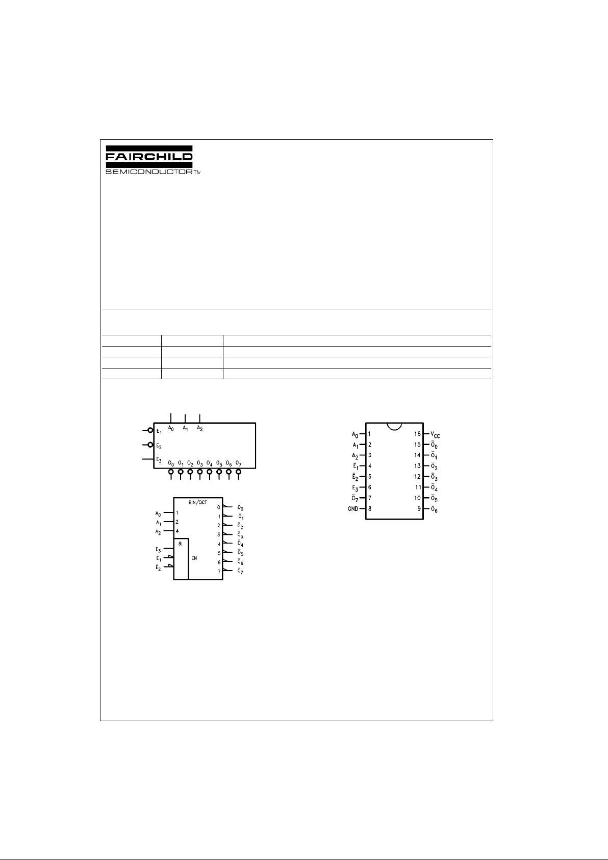
Logic Symbols
IEEE/IEC
Connection Diagram
Order Number Package Number Package Description
74F138SC M16A 16-Lead Small Outline Integrated Circuit (SOIC), JEDEC MS-012, 0.150 Narrow
74F138SJ M16D 16-Lead Small Outline Package (SOP), EIAJ TYPE II, 5.3mm Wide
74F138PC N16E 16-Lead Plastic Dual-In-Line Package (PDIP), JEDEC MS-001, 0.300 Wide
Page 2
www.fairchildsemi.com 2
74F138
Unit Loading/Fan Out
Tr uth Table
H = HIGH Voltage Level
L = LOW Voltage Level
X = Immaterial
Functional Description
The F138 high-speed 1-of-8 decoder/demultiplexer
accepts three binary weighted inputs (A
0, A1, A2
) and,
when enabled, provides eight mutually exclusive active
LOW outputs (O
0–O7
). The F138 features three Enable
inputs, two active LOW (E
1, E2
) and one active HIGH (E3).
All outputs will be HIGH unless E
1
and E2 are LOW and E
3
is HIGH. This multiple enable functi on allows easy parallel
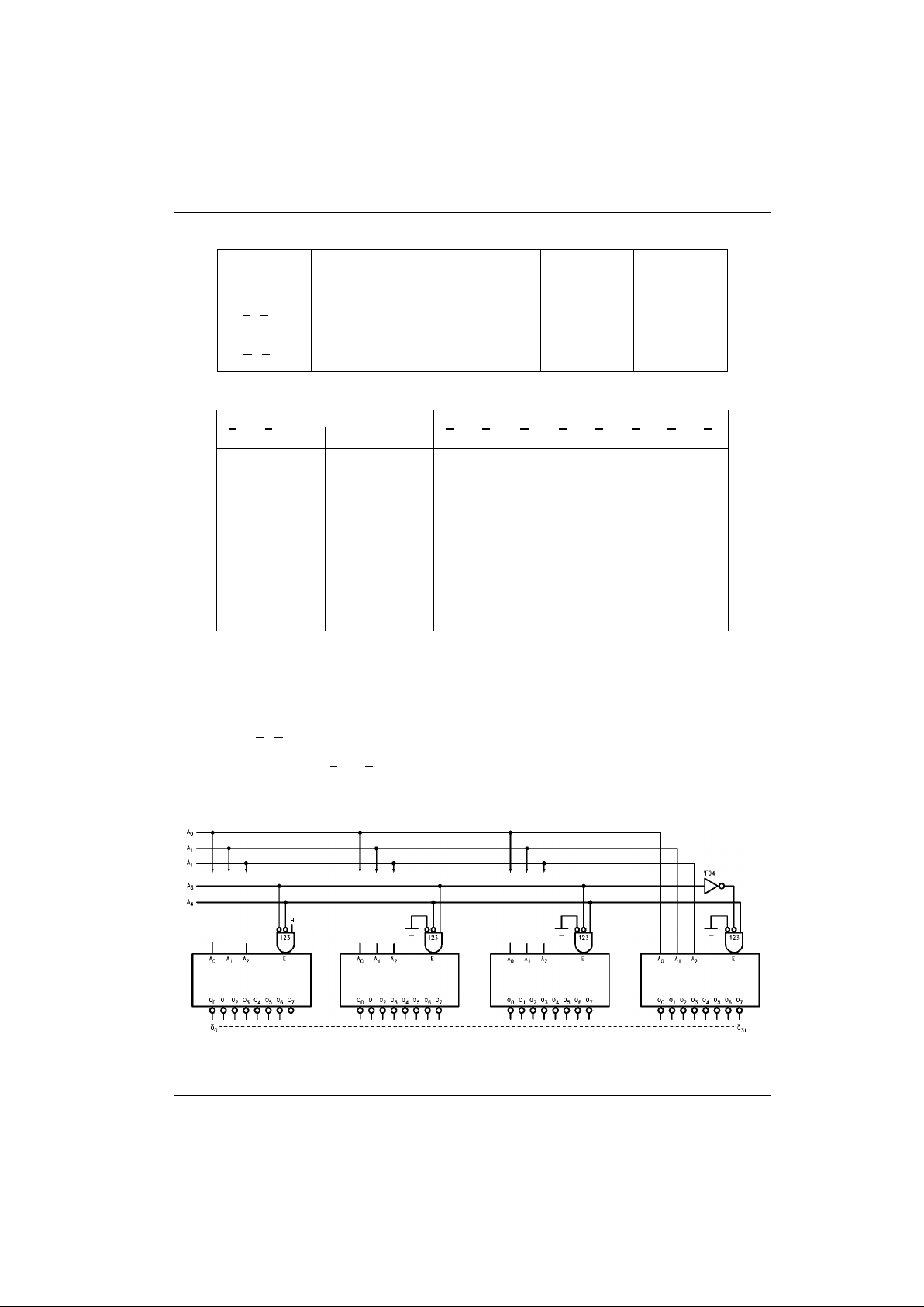
expansion of the de vice to a 1-of-32 (5 lines to 32 lines)
decoder with just f our F138 dev ices and one i nverte r (S ee
Figure 1). The F138 can be used as an 8-outpu t demultiplexer by using one of the active LOW Enable inputs as the
data input and the other Enable inputs as strobes. The
Enable inputs which are not used must be permanently tied
to their appropriate active HIGH or active LOW state.
FIGURE 1. Expans ion to 1-of-32 Decoding
Pin Names Description
U.L. Input I
IH/IIL
HIGH/LOW Output IOH/I
OL
A0–A
2
Address Inputs 1.0/1.0 20 µA/−0.6 mA
E
1
, E
2
Enable Inputs (Active LOW) 1.0/1.0 20 µA/−0.6 mA
E
3
Enable Input (Active HIGH) 1.0/1.0 20 µA/−0.6 mA
O
0–O7
Outputs (Active LOW) 50/33.3 −1 mA/20 mA
Inputs Outputs
E
1
E2E3A0A1A2O0O1O2 O3O4O5O6O
7
HXXXXXHHH HHHHH
XHXXXXHHHHHHHH
XXLXXXHH HHHHHH
LLHLLLLHHHHHHH
LLHHLLHL HHHHHH
LLHLHLHH L HHHHH
LLHHHLHH HLHHHH
LLHLLHHH H HLHHH
LLHHLHHH HHHLHH
LLHLHHHH HHHHLH
LLHHHHHH H HHHHL
Page 3

3 www.fairchildsemi.com
74F138
Logic Diagram
Please note that this diagram is provided only for the understanding of logic oper ations and sh ould not be used to estimate propagation delays.
Page 4

www.fairchildsemi.com 4
74F138
Absolute Maximum Ratings(Note 1) Recommended Operating
Conditions
Note 1: Absolute maximum ratings are values beyond which the device
may be damaged or have its useful life impaired. Functional operation
under these conditions is not implied.
Note 2: Either voltage lim it or current limit i s sufficient to protect inputs.
DC Electrical Characteristics
AC Electrical Characteristics
Storage Temperature −65°C to +150°C
Ambient Temperature under Bias −55°C to +125°C
Junction Temperature under Bias −55°C to +150°C
V
CC
Pin Potential to Ground Pin −0.5V to +7.0V
Input Voltage (Note 2) −0.5V to +7.0V
Input Current (Note 2) −30 mA to +5.0 mA
Voltage Applied to Output
in HIGH State (with V
CC
= 0V)
Standard Output −0.5V to V
CC
3-STATE Output −0.5V to +5.5V
Current Applied to Output
in LOW State (Max) twice the rated I
OL
(mA)
ESD Last Passing Voltage (Min) 4000V
Free Air Ambient Temperature 0°C to +70°C
Supply Voltage +4.5V to +5.5V
Symbol Parameter Min Typ Max Units
V
CC
Conditions
V
IH
Input HIGH Voltage 2.0 V Recognized as a HIGH Signal
V
IL
Input LOW Voltage 0.8 V Recognized as a LOW Signal
V
CD
Input Clamp Diode Voltage −1.2 V Min IIN = −18 mA
V
OH
Output HIGH 10% V
CC
2.5
VMin
IOH = −1 mA
Voltage 5% V
CC
2.7 IOH = −1 mA
V
OL
Output LOW 10% V
CC
0.5
V
Min IOL = 20 mA
Voltage
I
IH
Input HIGH
5.0 µAMaxVIN = 2.7V
Current
I
BVI
Input HIGH Current
7.0 µAMaxVIN = 7.0V
Breakdown Test
I
CEX
Output HIGH
50 µAMaxV
OUT
= V
CC
Leakage Current
V
ID
Input Leakage
4.75 V 0.0
IID = 1.9 µA
Test All Other Pins Grounded
I
OD
Output Leakage
3.75 µA0.0
V
IOD
= 150 mV
Circuit Current All Other Pins Grounded
I
IL
Input LOW Current −0.6 mA Max VIN = 0.5V
I
OS
Output Short-Circuit Current −60 −150 mA Max V
OUT
= 0V
I
CCH
Power Supply Current 13 20 mA Max VO = HIGH
I
CCL
Power Supply Current 13 20 mA Max VO = LOW
Symbol Parameter
TA = +25°CT
A
= 0°C to +70°C
Units
VCC = +5.0V VCC = +5.0V
CL = 50 pF CL = 50 pF
Min Typ Max Min Max
t
PLH
Propagation Delay 3.5 5.6 7.5 3.5 8.5
ns
t
PHL
An to O
n
4.0 6.1 8.0 4.0 9.0
t
PLH
Propagation Delay 3.5 5.4 7.0 3.5 8.0
ns
t
PHL
E1 or E2 to O
n
3.0 5.3 7.0 3.0 7.5
t
PLH
Propagation Delay 4.0 6.2 8.0 4.0 9.0
ns
t
PHL
E3 to O
n
3.5 5.6 7.5 3.5 8.5
Page 5

5 www.fairchildsemi.com
74F138
Physical Dimensions inches (millimeters) unless otherwise noted
16-Lead Small Outline Integrated Circuit (SOIC), JEDEC MS-012, 0.150 Narrow
Package Number M16A
16-Lead Small Outline Package (SOP), EIAJ TYPE II, 5.3mm Wide
Package Number M16D
Page 6

www.fairchildsemi.com 6
74F138 1-of-8 Decoder/Demultiplexer
Physical Dimensions inches (millimeters) unless otherwise noted (Continued)
16-Lead Plastic Dual-In-Line Package (PDIP), JEDEC MS-001, 0.300 Wide
Package Number N16E
Fairchild does no t assume any responsibility for use of an y circuitry d escribed, no c ircuit patent l icenses are impl ied and
Fairchild reserves the right at any time without notice to change said circuitry and specifications.
LIFE SUPPORT POLICY
FAIRCHILD’S PRODUCTS ARE NOT AUTHORIZED FOR USE AS CRITICAL COMPONENTS IN LIFE SUPPORT
DEVICES OR SYSTEMS WITHOUT THE EXPRESS WRITTEN APPROVAL OF THE PRESIDENT OF FAIRCHILD
SEMICONDUCTOR CORPORATION. As used herein:
1. Life support devices or systems are devices or systems
which, (a) are intended for surgical implant into the
body, or (b) support or sustain life, and (c) whose failure
to perform when properly used in accordance with
instructions for use provided in the labeling, can be reasonably expected to result in a sig nificant injury to the
user.
2. A critical com ponen t in any com pone nt of a life s upport
device or system w hose fa ilure to perform can be r easonably expected to cause the failure of the life support
device or system, or to affect its safety or effectiveness.
www.fairchildsemi.com
 Loading...