

Datasheet 74F1071SCX, 74F1071SC, 74F1071MTCX, 74F1071MTC, 74F1071MSAX Datasheet (Fairchild Semiconductor)
...Page 1
© 1999 Fairchild Semiconductor Corporation DS011685 www.fairchildsemi.com
October 1994
Revised August 1999
74F1071 18-Bit Undershoot/Overshoot Clamp
74F1071
18-Bit Undershoot/Overshoot Clamp
and ESD Protection Device
General Description
The 74F1071 is an 18-bit undershoot/overshoot clamp
which is designed to limit bus volt ages and also to prot ect
more sensitive devices from electrical overstress due to
electrostatic discharge (ESD). The inputs of the device
aggressively clamp vo ltage excursions nominally at 0.5V
below and 7V above ground.
Features
■ 18-bit array structure in 20-pin package
■ FAST Bipolar voltage clamping action
■ Dual center pin grounds for min inductance
■ Robust design for ESD protection
■ Low input capacitance
■ Optimum voltage clamping for 5V CMOS/TTL
applications
Ordering Code:
Devices also availab le in Tape and Reel. Specify by appending th e s uffix let t er “X” to the ordering cod e.
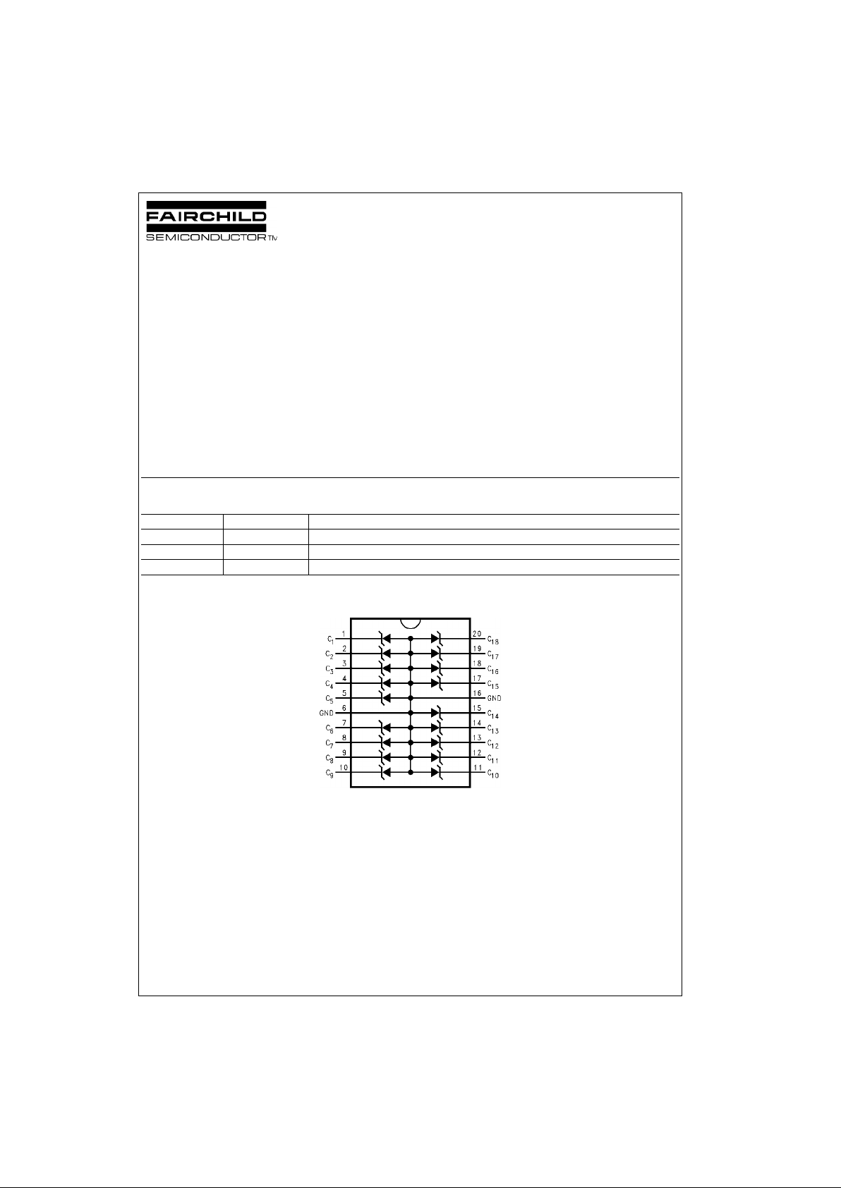
Connection Diagram
Note: Simplified Comp onent Representatio n
FAST is a regist ered trademark of Fair c hild Semiconductor C orporation.
Order Number Package Number Package Description
74F1071SC M20B 20-Lead Small Outline Integrated Circuit (SOIC), JEDEC MS-013, 0.300 Wide
74F1071MSA MSA20 20-Lead Shrink Small Outline Package (SSOP), EIAJ TYPE II, 5.3mm Wide
74F1071MTC MTC20 20-Lead Thin Shrink Small Outline Package (TSSOP), JEDEC MO-153, 4.4mm Wide
Page 2
www.fairchildsemi.com 2
74F1071
Absolute Maximum Ratings(Note 1) Recommended Operating
Conditions
Note 1: Absolute maximum ratings are DC values beyond which the device
may be damaged or have its useful life impaired. Functional operation
under these conditi ons is not implied.
Note 2: Voltage ratings may be e xceeded if curren t ratings and juncti on
temperature and pow er consumption rati ngs are not exceeded.
Note 3: ESD Rating for Dire ct contact discharge usi ng ESD Simulation
Tester. Higher rating may be realized in the actual application.
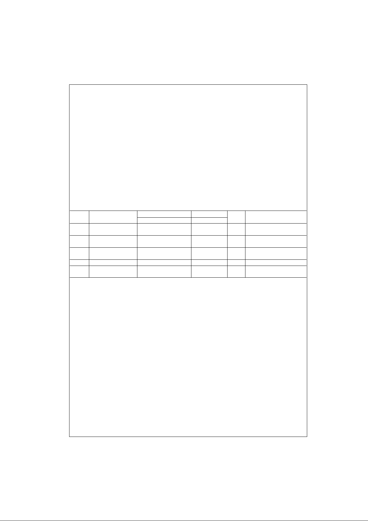
DC Electrical Characteristics
Storage Temperature −65°C to +150°C
Ambient Temperature under Bias −65°C to +125°C
Junction Temperature under Bias −65°C to +150°C
Input Voltage (Note 2) −0.5V to +6V
Input Current (Note 2) −200 mA to +50 mA
ESD (Note 3)
Human Body Model
(MIL-STD-883D method 3015.7) ±10 kV
IEC 801-2 ±6 kV
Machine Model (EIAJIC-121-1981) ±2 kV
DC Latchup Source Current
(JEDEC Method 17) ±500 mA
Package Power Dissipation @+70°C
SOIC Package 800 mW
Free Air Ambient Temperature 0°C to +70°C
Reverse Bias Voltage 0V to 5.25 V
DC
Thermal Resistance (θJA in Free Air)
SOIC Package 100°C/W
SSOP Package 110°C/W
Symbol Parameter
TA = +25°CT
A
= 0°C to +70°C
Units Conditions
Min Typ Max Min Max
I
IH
Input HIGH Current 1.5 10 50
µA
VIN = 5.25V; Untested Input @ GND
320 100 VIN = 5.5V; Untested Input @ GND
V
Z
Reverse Voltage 6.6 6.9 7.2 5.9 7.7
V
IZ = 1 mA; Untested Inputs @ GND
7.1 7.5 8.0 IZ = 50 mA; Untested Inputs @ GND
V
F
Forward Voltage −0.3 −0.6 −0.9 −0.3 −0.9
V
IF = −18 mA; Untested Inputs @ 5V
−0.5 −1.1 −1.5 −0.5 −1.5 IF = −200 mA; Untested Inputs @ 5V
I
CT
Adjacent Input Crosstalk 3 %
C
IN
Input Capacitance 25
pF
V
BIAS
= 0 V
DC
(small signal @ 1 MHz) 13 V
BIAS
= 5 V
DC
Page 3

3 www.fairchildsemi.com
74F1071
DC Electrical Characteristics
Ty pical Forward and Reverse V/I
Characteristics
Typical Reverse Conduction
Characteristics
Typical Forward Conduction
Characteristics
ESD Network CZ RZ
Human Body Model 100 pF 1500Ω
IEC 801-2 150 pF 330Ω
Simulated ESD Voltage Clamping Test Circuit
Page 4

www.fairchildsemi.com 4
74F1071
DC Electrical Characteristics (Continued)
Unclamped + 1 KV ESD Voltage
Waveform (IEC801-2 Network)
Clamped + 1 KV ESD Voltage
Waveform (IEC801-2 Network)
Unclamped - 1 KV ESD Voltage
Waveform (IEC801-2 Network)
Clamped - 1 KV ESD Voltage
Waveform (IEC801-2 Network)
Typical Application
74F1071 ESD Protection of ASIC on User Port
Page 5

5 www.fairchildsemi.com
74F1071
Physical Dimensions inches (millimeters) unless otherwise noted
20-Lead Small Outline Integrated Circuit (SOIC), JEDEC MS-013, 0.300 Wide
Package Number M20B
20-Lead Shrink Small Outline Package (SSOP), EIAJ TYPE II, 5.3mm Wide
Package Number MSA20
Page 6

www.fairchildsemi.com 6
74F1071 18-Bit Undershoot/Overshoot Clamp
Physical Dimensions inches (millimeters) unless otherwise noted (Continued)
20-Lead Thin Shrink Small Outline Package (TSSOP), JEDEC MO-153, 4.4mm Wide
Package Number MTC20
Fairchild does not assume any responsibility for use of any circuitry described, no circuit pate nt licenses are implied and
Fairchild reserves the right at any time without notice to change said circuitry and specifications.
LIFE SUPPORT POLICY
FAIRCHILD’S PRODUCTS ARE NOT AUTHORIZED FOR USE AS CRITICAL COMPONENTS IN LIFE SUPPORT
DEVICES OR SYSTEMS WITHOUT THE EXPRESS WRITTEN APPROVAL OF THE PRESIDENT OF FAIRCHILD
SEMICONDUCTOR CORPORATION. As used herein:
1. Life support devices or systems are devices or syste ms
which, (a) are intended for surgical implant into the
body, or (b) support or sustain life, and (c) whose failure
to perform when properly used in accordance with
instructions for use provided in the labeling, can be reasonably expected to result in a significant inju ry to the
user.
2. A critical component i n any compon ent of a lif e support
device or system whose failu re to perform can be reasonably expected to ca use the fa i lure of the life su pp ort
device or system, or to affect its safety or effectiveness.
www.fairchildsemi.com
 Loading...