

Page 1

INTEGRATED CIRCUITS
DATA SH EET
74AUC1G08
Single 2-input AND gate
Preliminary specification
File under Integrated Circuits, IC24
2002 Nov 12
Page 2
Philips Semiconductors Preliminary specification
Single 2-input AND gate 74AUC1G08
FEATURES
• Wide supply voltage range from 0.8 to 2.7 V
• Performance optimised for VCC= 1.8 V
• High noise immunity
• Complies with JEDEC standard:
– JESD76 (1.65 to 1.95 V)
• ESD protection:
– HBM EIA/JESD22-A114-A exceeds 2000 V
– MM EIA/JESD22-A115-A exceeds 200 V
• 8 mA output drive (VCC= 1.65 V)
DESCRIPTION
The 74AUC1G08 is a high-performance, low-power,
low-voltage, Si-gate CMOS device.
Schmitt-trigger action at all inputs makes the circuit
tolerant for slower input rise and fall time.
This device is fully specified for partial power-down
applications usingI
. The I
off
circuitry disablesthe output,
off
preventing the damaging current backflow through the
device when it is powered down.
The 74AUC1G08 provides the single 2-input AND
function.
• CMOS low power consumption
• Latch-up performance exceeds 250 mA
• 3.3 V tolerant inputs/outputs
• SC-88A and SC-74A package.
QUICK REFERENCE DATA
GND = 0 V; T
=25°C; input slewrate ≥ 1 V/ns.
amb
SYMBOL PARAMETER CONDITIONS TYPICAL UNIT
t
PHL/tPLH
propagation delay inputs A and B to
output Y
VCC= 0.8 V; CL= 15 pF; RL=2kΩ 4.7 ns
VCC= 1.2 V; CL= 15 pF; RL=2kΩ 1.9 ns
VCC= 1.5 V; CL= 15 pF; RL=2kΩ 1.4 ns
V
= 1.8 V; CL= 30 pF; RL=1 kΩ 1.4 ns
CC
VCC= 2.5 V; CL= 30 pF; RL= 500 Ω 1.2 ns
C
I
C
PD
input capacitance 4 pF
power dissipation capacitance per buffer VCC= 1.8 V; notes 1 and 2 14 pF
Notes
1. C
is used to determine the dynamic power dissipation (PDin µW).
PD
PD=CPD× V
2
× fi+(CL× V
CC
2
× fo) where:
CC
fi= input frequency in MHz;
fo= output frequency in MHz;
CL= output load capacitance in pF;
VCC= supply voltage in Volts.
2. The condition is VI= GND to VCC.
2002 Nov 12 2
Page 3
Philips Semiconductors Preliminary specification
Single 2-input AND gate 74AUC1G08
FUNCTION TABLE
See note 1.
INPUT OUTPUT
ABY
LLL
LHL
HLL
HHH
Note
1. H = HIGH voltage level;
L = LOW voltage level.
ORDERING INFORMATION
PACKAGE
TYPE NUMBER
74AUC1G08GW −40 to +85 °C 5 SC-88A plastic SOT353 FE
74AUC1G08GV −40 to +85 °C 5 SC-74A plastic SOT753 F08
TEMPERATURE
RANGE
PINS PACKAGE MATERIAL CODE MARKING
PINNING
handbook, halfpage
PIN SYMBOL DESCRIPTION
1 B data input B
2 A data input A
3 GND ground (0 V)
4 Y data output Y
5V
B
A
GND
CC
1
2
3
5
08
4
MNA112
V
CC
Y
supply voltage
handbook, halfpage
1
B
2
A
Y
MNA113
4
Fig.1 Pin configuration.
2002 Nov 12 3
Fig.2 Logic symbol.
Page 4
Philips Semiconductors Preliminary specification
Single 2-input AND gate 74AUC1G08
handbook, halfpage
1
2
&
4
MNA114
Fig.3 IEE/IEC logic symbol.
A
Y
B
Fig.4 Logic diagram.
RECOMMENDED OPERATING CONDITIONS
SYMBOL PARAMETER CONDITIONS MIN. MAX. UNIT
V
CC
V
I
V
O
supply voltage 0.8 2.7 V
input voltage 0 2.7 V
output voltage active mode 0 V
CC
V
VCC= 0 V; Power-down mode 0 2.7 V
T
amb
operating ambient temperature −40 +85 °C
tr,tf (∆t/∆f) input rise and fall times 0 20 ns/V
LIMITING VALUES
In accordance with theAbsolute Maximum Rating System (IEC 60134); voltages are referenced to GND (ground = 0 V).
SYMBOL PARAMETER CONDITIONS MIN. MAX. UNIT
V
CC
I
IK
V
I
I
OK
V
O
supply voltage −0.5 +3.6 V
input diode current VI<0 −−50 mA
input voltage note 1 −0.5 +3.6 V
output diode current VO>VCC or VO<0 −±50 mA
output voltage active mode; notes 1 and 2 −0.5 VCC+ 0.5 V
Power-down mode; notes 1 and 2 −0.5 +3.6 V
I
O
ICC, I
T
stg
P
D
GND
output source or sink current VO=0toV
CC
−±60 mA
VCC or GND current −±100 mA
storage temperature −65 +150 °C
power dissipation per package for temperature range from
− 250 mW
−40 to +85 °C
Notes
1. The input and output voltage ratings may be exceeded if the input and output current ratings are observed.
2. When VCC=0 (Powered-down mode), the output voltage can be 2.7 V in normal operation.
2002 Nov 12 4
Page 5

Philips Semiconductors Preliminary specification
Single 2-input AND gate 74AUC1G08
DC CHARACTERISTICS
At recommended operating conditions; voltages are referenced to GND (ground = 0 V).
SYMBOL PARAMETER
V
IH
HIGH-level input
voltage
V
IL
LOW-level input
voltage
V
OH
HIGH-leveloutput
voltage
V
OL
LOW-level output
voltage
I
I
input leakage
current
I
off
power OFF
leakage current
I
CC
quiescent supply
current
TEST CONDITIONS T
OTHER VCC (V)
MIN. TYP.
0.8 V
CC
(°C)
amb
−40 to +85
(1)
MAX.
−− V
UNIT
1.1 to 2.3 0.65 × VCC−− V
2.3 to 2.7 1.7 −− V
0.8 −−GND V
1.1 to 2.3 −−0.35 × VCCV
2.3 to 2.7 −−0.7 V
VI=VIHor VIL; IO= −100 µA 0.8 to 2.7 VCC− 0.1 −− V
VI=VIHor VIL; IO=− 700 µA 0.8 − 0.55 − V
VI=VIHor VIL; IO=− 3 mA 1.1 VCC− 0.3 −− V
VI=VIHor VIL; IO= −5 mA 1.5 VCC− 0.4 −− V
VI=VIHor VIL; IO= −8 mA 1.65 VCC− 0.45 −− V
VI=VIHor VIL; IO= −9 mA 2.3 1.8 −− V
VI=VIHor VIL; IO= 100 µA 0.8 to 2.7 −−0.2 V
VI=VIHor VIL; IO= 700 µA 0.8 − 0.25 − V
VI=VIHor VIL; IO= 3 mA 1.1 −−0.3 V
VI=VIHor VIL; IO= 5 mA 1.5 −−0.4 V
VI=VIHor VIL; IO= 8 mA 1.65 −−0.45 V
VI=VIHor VIL; IO= 9 mA 2.3 −−0.6 V
VI=VCCor GND 0 to 2.7 −±0.1 ±5 µA
VIor VO= 2.7 V 0 −±0.1 ±10 µA
VI=VCCor GND; IO= 0 0.8 to 2.7 − 0.1 10 µA
Note
1. All typical values are measured at T
amb
=25°C.
2002 Nov 12 5
Page 6
Philips Semiconductors Preliminary specification
Single 2-input AND gate 74AUC1G08
AC CHARACTERISTICS
GND = 0 V; input slewrate≥ 1 V/ns.
SYMBOL PARAMETER
t
PHL/tPLH
propagation delay
inputs A and B to output Y
AC WAVEFORMS
WAVEFORMS VCC (V) CL(pF)
see
Figs 5 and 6
handbook, halfpage
A, B input
TEST CONDITIONS T
−40 to +85
MIN. TYP. MAX.
0.8 15 − 4.7 ns
1.1 to 1.3 15 0.9 1.9 3.3 ns
1.4 to 1.6 15 0.6 1.4 2.3 ns
1.65 to 1.95 30 0.7 1.4 2.4 ns
2.3 to 2.7 30 0.5 1.2 2.0 ns
V
M
t
PHL
t
PLH
amb
(°C)
UNIT
Y output
V
M
INPUT
V
CC
0.8 to 2.7 V 0.5 × VCCV
VOL and VOH are typical output voltage drop that occur with the output load.
V
M
CC
V
I
Slewrate
≥ 1 V/ns
Fig.5 Inputs A, B to output Y propagation delay times.
MNA167
2002 Nov 12 6
Page 7
Philips Semiconductors Preliminary specification
Single 2-input AND gate 74AUC1G08
handbook, full pagewidth
V
CC
PULSE
GENERATOR
V
I
D.U.T.
R
T
V
V
V
CC
<1.65 V V
1.65 to 1.95 V V
2.3 to 2.7 V V
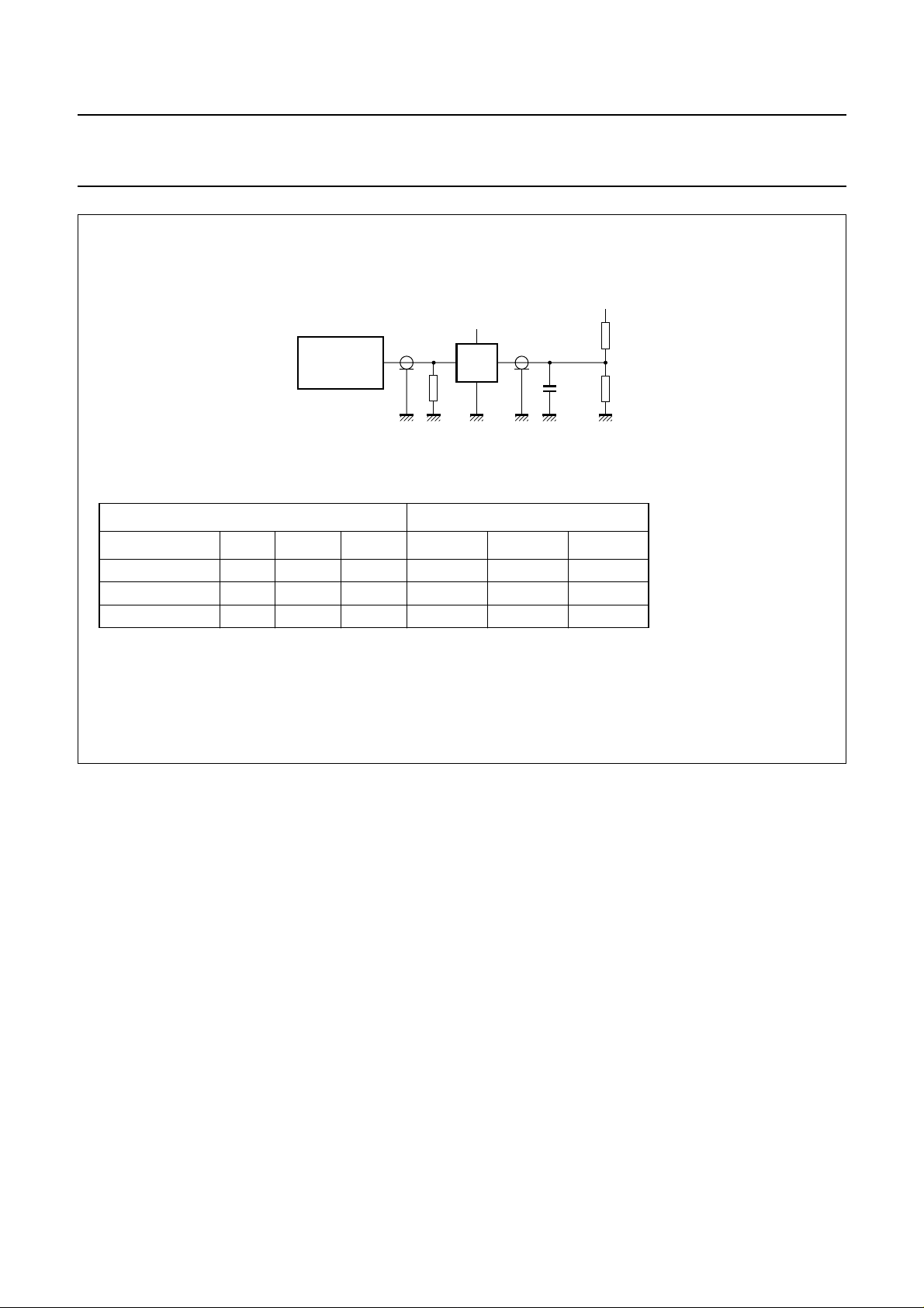
Definitions for test circuits:
RL= Load resistor.
CL= Load capacitance including jig and probe capacitance (see Chapter “AC characteristics”).
RT= Termination resistance should be equal to the output impedance Zo of the pulse generator.
CC
CC
CC
V
I
C
L
R
T
L
PLH/TPHLTPZH/TPHZTPZL/TPLZ
15 pF 2 kΩ open GND 2 × V
30 pF 1 kΩ open GND 2 × V
30 pF 0.5 kΩ open GND 2 × V
Fig.6 Load circuitry for switching times.
O
EXT
V
EXT
R
L
C
R
L
L
MNA616
CC
CC
CC
2002 Nov 12 7
Page 8
Philips Semiconductors Preliminary specification
Single 2-input AND gate 74AUC1G08
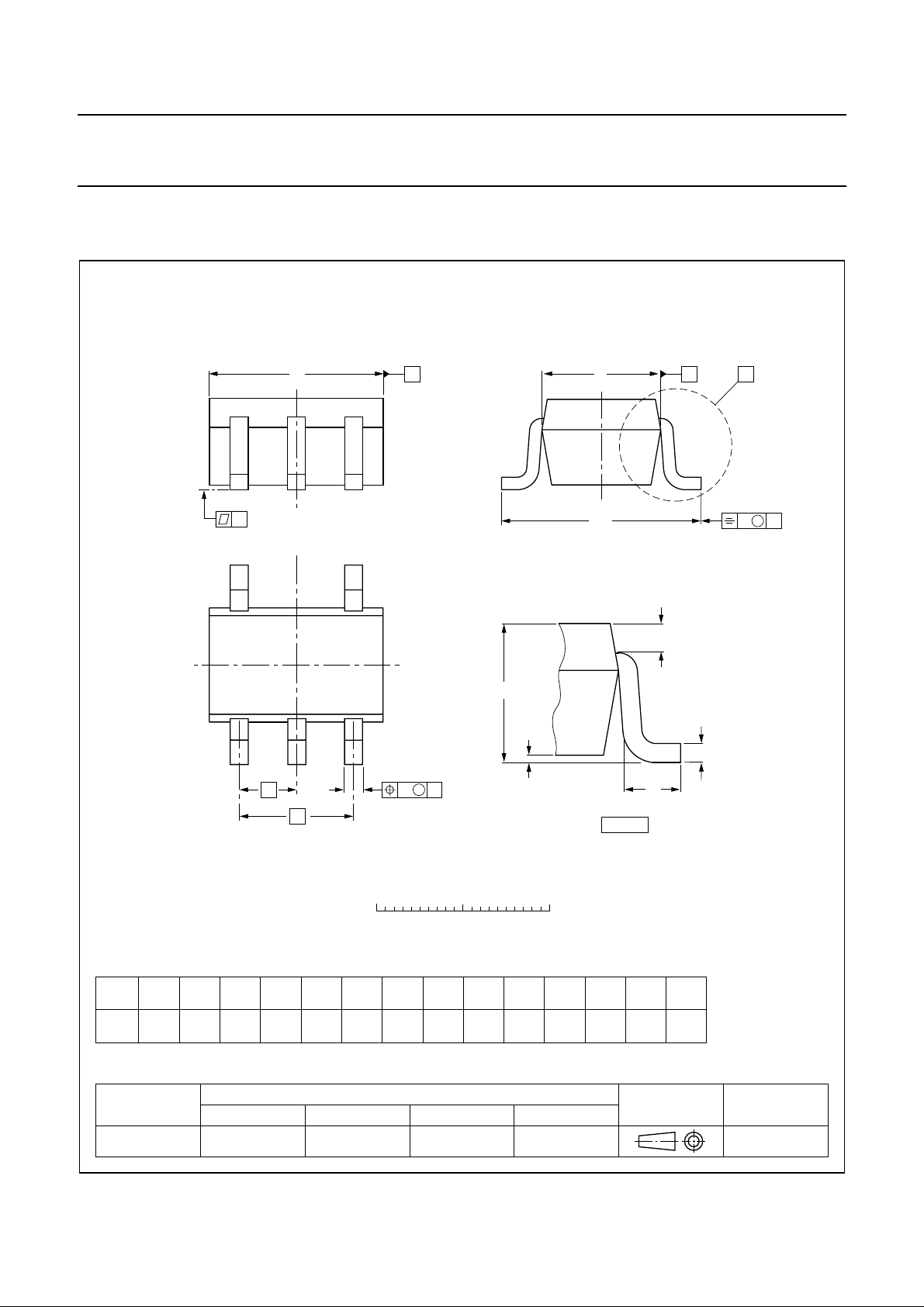
PACKAGE OUTLINE
Plastic surface mounted package; 5 leads SOT353
D
y
132
e
1
e
E
H
E
AB
X
v M
A
45
Q
A
A
1
c
b
p
wBM
detail X
L
p
0 1 2 mm
scale
DIMENSIONS (mm are the original dimensions)
A
UNIT
mm
A
1.1
0.8
OUTLINE
VERSION
SOT353
max
0.1
1
b
cD
p
0.30
0.25
0.20
0.10
IEC JEDEC EIAJ
2.2
1.8
(2)
E
1.35
1.3
1.15
REFERENCES
e
e
1
0.65
2002 Nov 12 8
H
2.2
2.0
L
Qywv
p
E
0.45
0.15
0.25
0.15
0.2 0.10.2
EUROPEAN
PROJECTION
ISSUE DATE
97-02-28SC-88A
Page 9
Philips Semiconductors Preliminary specification
Single 2-input AND gate 74AUC1G08
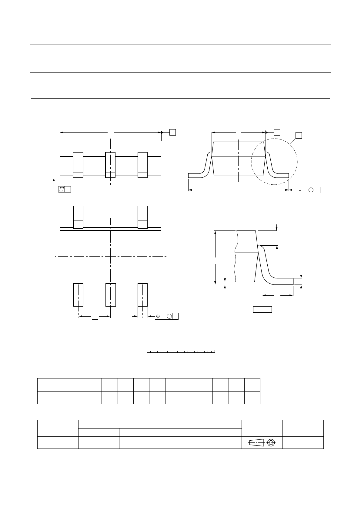
Plastic surface mounted package; 5 leads SOT753
D
y
E
H
E
AB
X
v M
A
45
Q
A
A
1
c
132
L
p
3.1
2.7
b
p
wBM
0 1 2 mm
scale
H
e
E
1.7
0.95
1.3
REFERENCES
E
3.0
2.5
e
DIMENSIONS (mm are the original dimensions)
A
UNIT
mm
A
0.100
1.1
0.013
0.9
OUTLINE
VERSION
SOT753 SC-74A
b
cD
p
1
0.40
0.26
0.25
0.10
IEC JEDEC JEITA
2002 Nov 12 9
L
0.6
0.2
detail X
Qywv
p
0.33
0.23
0.2 0.10.2
EUROPEAN
PROJECTION
ISSUE DATE
02-04-16
Page 10

Philips Semiconductors Preliminary specification
Single 2-input AND gate 74AUC1G08
SOLDERING
Introduction to soldering surface mount packages
This text gives a very brief insight to a complex
technology. A more in-depth account of soldering ICs can
be found in our
Packages”
There is no soldering method that is ideal for all surface
mount IC packages. Wave soldering can still be used for
certain surface mount ICs, but it is not suitable for fine
pitch SMDs. In these situations reflow soldering is
recommended.
Reflow soldering
Reflow soldering requires solder paste (a suspension of
fine solder particles, flux and binding agent) to be applied
to the printed-circuit board by screen printing, stencilling
or pressure-syringe dispensing before package
placement.
Several methods exist for reflowing; for example,
convection or convection/infrared heating in a conveyor
type oven. Throughput times (preheating, soldering and
cooling) vary between 100 and 200 seconds depending
on heating method.
Typical reflow peak temperatures range from
215 to 250 °C. The top-surface temperature of the
packages should preferable be kept below 220 °C for
thick/large packages, and below 235 °C for small/thin
packages.
Wave soldering
Conventional single wave soldering is not recommended
for surface mount devices (SMDs) or printed-circuit
boards with a high component density, as solder bridging
and non-wetting can present major problems.
To overcome these problems the double-wave soldering
method was specifically developed.
“Data Handbook IC26; Integrated Circuit
(document order number 9398 652 90011).
If wave soldering is used the following conditions must be
observed for optimal results:
• Use a double-wave soldering method comprising a
turbulent wave with high upward pressure followed by
a smooth laminar wave.
• For packages with leads on two sides and a pitch (e):
– larger than or equal to 1.27 mm, the footprint
longitudinal axis is preferred to be parallel to the
transport direction of the printed-circuit board;
– smaller than 1.27 mm, the footprint longitudinal axis
must be parallel to the transport direction of the
printed-circuit board.
The footprint must incorporate solder thieves at the
downstream end.
• For packages with leads on four sides, the footprint
must be placed at a 45° angle to the transport direction
of the printed-circuit board. The footprint must
incorporate solder thieves downstream and at the side
corners.
During placement and before soldering, the package
must be fixed with a droplet of adhesive. The adhesive
can be applied by screen printing, pin transfer or syringe
dispensing. The package can be soldered after the
adhesive is cured.
Typical dwell time is 4 seconds at 250 °C.
A mildly-activated flux will eliminate the need for removal
of corrosive residues in most applications.
Manual soldering
Fix the component by first soldering two
diagonally-oppositeend leads. Use a low voltage (24 Vor
less) soldering iron applied to the flat part of the lead.
Contact time must be limited to 10 seconds at up to
300 °C.
When using a dedicated tool, all other leads can be
soldered in one operation within 2 to 5 seconds between
270 and 320 °C.
2002 Nov 12 10
Page 11

Philips Semiconductors Preliminary specification
Single 2-input AND gate 74AUC1G08
Suitability of surface mount IC packages for wave and reflow soldering methods
PACKAGE
WAVE REFLOW
(1)
BGA, HBGA, LFBGA, SQFP, TFBGA not suitable suitable
SOLDERING METHOD
HBCC, HLQFP, HSQFP, HSOP, HTQFP, HTSSOP, HVQFN, SMS not suitable
(3)
PLCC
, SO, SOJ suitable suitable
LQFP, QFP, TQFP not recommended
SSOP, TSSOP, VSO not recommended
(2)
(3)(4)
(5)
suitable
suitable
suitable
Notes
1. All surface mount (SMD) packages are moisture sensitive. Depending upon the moisture content, the maximum
temperature (with respect to time) and body size of the package, there is a risk that internal or external package
cracks may occur due to vaporization of the moisture in them (the so called popcorn effect). For details, refer to the
Drypack information in the
“Data Handbook IC26; Integrated Circuit Packages; Section: Packing Methods”
.
2. These packages are not suitable for wave soldering as a solder joint between the printed-circuit board and heatsink
(at bottom version) can not be achieved, and as solder may stick to the heatsink (on top version).
3. If wave soldering is considered, then the package must be placed at a 45° angle to the solder wave direction.
The package footprint must incorporate solder thieves downstream and at the side corners.
4. Wave soldering is only suitable for LQFP, TQFP and QFP packages with a pitch (e) equal to or larger than 0.8 mm;
it is definitely not suitable for packages with a pitch (e) equal to or smaller than 0.65 mm.
5. Wave soldering is only suitable for SSOP and TSSOP packages with a pitch (e) equal to or larger than 0.65 mm; it is
definitely not suitable for packages with a pitch (e) equal to or smaller than 0.5 mm.
2002 Nov 12 11
Page 12

Philips Semiconductors Preliminary specification
Single 2-input AND gate 74AUC1G08
DATA SHEET STATUS
DATA SHEET STATUS
Objective specification Development This data sheet contains the design target or goal specifications for
Preliminary specification Qualification This data sheet contains preliminary data, and supplementary data will be
Product specification Production This data sheet contains final specifications. Philips Semiconductors
Note
1. Please consult the most recently issued data sheet before initiating or completing a design.
DEFINITIONS
Short-form specification The data in a short-form
specification is extracted from a full data sheet with the
same type number and title. For detailed information see
the relevant data sheet or data handbook.
LimitingvaluesdefinitionLimitingvaluesgiven are in
accordance with the Absolute Maximum Rating System
(IEC 60134). Stress above one or more of the limiting
values may cause permanent damage to the device.
These are stress ratings only and operation of the device
at these or at any other conditions above those given in
the Characteristics sections of the specification is not
implied. Exposure to limiting values for extended periods
may affect device reliability.
Application information Applications that are
described herein for any of these products are for
illustrative purposes only. Philips Semiconductors make
no representation or warranty that such applications will
be suitable for the specified use without further testing or
modification.
PRODUCT
STATUS
DEFINITIONS
product development. Specification may change in any manner without
notice.
published at a later date. Philips Semiconductors reserves the right to
make changes at any time without notice in order to improve design and
supply the best possible product.
reserves the right to make changes at any time without notice in order to
improve design and supply the best possible product.
DISCLAIMERS
Life support applications These products are not
designed for use in life support appliances, devices, or
systems where malfunction of these products can
reasonably be expected to result in personal injury.
Philips Semiconductors customers using or selling these
products for use in such applications do so at their own
risk and agree to fully indemnify Philips Semiconductors
for any damages resulting from such application.
Right to make changes Philips Semiconductors
reserves the right to make changes, without notice, in the
products, including circuits, standard cells, and/or
software, described or contained herein in order to
improve design and/or performance. Philips
Semiconductors assumes no responsibility or liability for
the use of any of these products, conveys no licence or
title under any patent, copyright, or mask work right to
these products, and makes no representations or
warranties that these products are free from patent,
copyright, or mask work right infringement, unless
otherwise specified.
(1)
2002 Nov 12 12
 Loading...