

Page 1

INTEGRATED CIRCUITS
74ALVT16245
2.5V/3.3V ALVT 16-bit transceiver
(3-State)
Product specification
Supersedes data of 1995 Nov 01
IC23 Data Handbook
1998 Feb 13
Page 2

Philips Semiconductors Product specification
SYMBOL
PARAMETER
UNIT
74AL VT162452.5V/3.3V 16-bit transceiver (3-State)
FEA TURES
•16-bit bidirectional bus interface
•5V I/O Compatible
•3-State buffers
•Output capability: +64mA/–32mA
•TTL input and output switching levels
•Bus-hold data inputs eliminate the need for external pull-up
resistors to hold unused inputs
•Live insertion/extraction permitted
•Power-up 3-State
•No bus current loading when output is tied to 5V bus
•Latch-up protection exceeds 500mA per JEDEC Std 17
•ESD protection exceeds 2000V per MIL STD 883 Method 3015
and 400V per Machine Model
QUICK REFERENCE DATA
t
PLH
t
PHL
C
C
I
CCZ
IN
I/O
Propagation delay
nAx to nBx or nBx to nAx
Input capacitance DIR, OE VI = 0V or V
I/O pin capacitance V
Total supply current Outputs disabled 40 70 µA
CL = 50pF
= 0V or V
I/O
DESCRIPTION
The 74ALVT16245 is a high-performance BiCMOS product
designed for V
to 5V .
This device is a 16-bit transceiver featuring non-inverting 3-State
bus compatible outputs in both send and receive directions. The
control function implementation minimizes external timing
requirements. The device features an Output Enable (OE
easy cascading and a Direction (DIR) input for direction control.
CONDITIONS
T
amb
CC
CC
operation at 2.5V or 3.3V with I/O compatibility up
CC
TYPICAL
= 25°C
2.5V 3.3V
1.7
1.9
1.5
1.5
3 3 pF
9 9 pF
) input for
ns
ORDERING INFORMATION
PACKAGES TEMPERATURE RANGE OUTSIDE NORTH AMERICA NORTH AMERICA DWG NUMBER
48-Pin Plastic SSOP Type III –40°C to +85°C 74ALVT16245 DL AV16245 DL SOT370-1
48-Pin Plastic TSSOP Type II –40°C to +85°C 74ALVT16245 DGG AV16245 DGG SOT362-1
LOGIC SYMBOL
1
1DIR
47
1A0
46
1A1
44
1A2
43
1A3
41
1A4
40
1A5
38
1A6
37 12
1A7
24
2DIR
48
1OE
2
1B0
3
1B1
5
1B2
6
1B3
8
1B4
9
1B5
11
1B6
1B7
36
2A0
35
2A1
33
2A2
32
2A3
30
2A4
29
2A5
27
2A6
26 23
2A7
25
2OE
13
2B0
14
2B1
16
2B2
17
2B3
19
2B4
20
2B5
22
2B6
2B7
LOGIC SYMBOL (IEEE/IEC)
48
1
47
46
44 5
43 6
41 8
40 9
38 11
37 12
G3
3 EN1 (BA)
3 EN2 (AB)
∇ 1
2
2 ∇
3
25
24
36
35
33 16
32 17
30 19
29 20
27 22
26 23
G3
3 EN1 (BA)
3 EN2 (AB)
∇ 1
2 ∇
13
14
SW00022
SA00021
1998 Feb 13 853-1817 18959
2
Page 3

Philips Semiconductors Product specification
I
DC output current
mA
74ALVT162452.5V/3.3V 16-bit transceiver (3-State)
PIN CONFIGURA TION
1
1DIR
2
1B0
3
1B1
GND
4
5
1B2
6
1B3
7
V
CC
8
1B4
1B5
9
GND
10
1B6
11
1B7
12
2B0
13
2B1
14
GND
15
16
2B2
2B3
17
18
V
CC
2B4
19
20
2B5
21
GND
22
2B6
23
2B7
24
2DIR
48
47
46
45
44
43
42
41
40
39
38
37
36
35
34
33
32
31
30
29
28
27
26
25
SA00020
1OE
1A0
1A1
GND
1A2
1A3
V
CC
1A4
1A5
GND
1A6
1A7
2A0
2A1
GND
2A2
2A3
V
CC
2A4
2A5
GND
2A6
2A7
2OE
PIN DESCRIPTION
PIN NUMBER SYMBOL NAME AND FUNCTION
1, 24 nDIR Direction control input
47, 46, 44, 43,
41, 40, 38, 37,
36, 35, 33, 32,
nA0 – nA7 Data inputs/outputs (A side)
30, 29, 27, 26
2, 3, 5, 6, 8, 9,
11, 12, 13, 14,
16, 17, 19, 20,
nB0 – nB7 Data inputs/outputs (B side)
22, 23
25, 48 nOE Output enable input (active-Low)
4, 10, 15, 21,
28, 34, 39, 45
7, 18, 31, 42 V
GND Ground (0V)
CC
Positive supply voltage
FUNCTION TABLE
INPUTS INPUTS/OUTPUTS
nOE nDIR nAx nBx
L L nAx = nBx Inputs
L H Inputs nBx = nAx
H X Z Z
H = High voltage level
L = Low voltage level
X = Don’t care
Z = High Impedance “off” state
ABSOLUTE MAXIMUM RATINGS
SYMBOL
V
CC
I
IK
V
I
I
OK
V
OUT
OUT
T
stg
DC supply voltage –0.5 to +4.6 V
DC input diode current VI < 0 –50 mA
DC input voltage
DC output diode current VO < 0 –50 mA
DC output voltage
p
Storage temperature range –65 to +150 °C
PARAMETER CONDITIONS RATING UNIT
3
3
1, 2
–0.5 to +7.0 V
Output in Off or High state –0.5 to +7.0 V
Output in Low state 128
Output in High state –64
NOTES:
1. Stresses beyond those listed may cause permanent damage to the device. These are stress ratings only and functional operation of the
device at these or any other conditions beyond those indicated under “recommended operating conditions” is not implied. Exposure to
absolute-maximum-rated conditions for extended periods may affect device reliability .
2. The performance capability of a high-performance integrated circuit in conjunction with its thermal environment can create junction
temperatures which are detrimental to reliability. The maximum junction temperature of this integrated circuit should not exceed 150°C.
3. The input and output negative voltage ratings may be exceeded if the input and output clamp current ratings are observed.
1998 Feb 13
3
Page 4

Philips Semiconductors Product specification
SYMBOL
PARAMETER
UNIT
I
mA
VOHHigh-level out ut voltage
V
VOLLow–level out ut voltage
V
4
V
6V; V
V
Data ins
4
0.5
10
Bus Hold current
A or B ports
6
74ALVT162452.5V/3.3V 16-bit transceiver (3-State)
RECOMMENDED OPERATING CONDITIONS
2.5V RANGE LIMITS 3.3V RANGE LIMITS
MIN MAX MIN MAX
V
CC
V
V
V
I
OH
OL
∆t/∆v Input transition rise or fall rate; Outputs enabled 10 10 ns/V
T
amb
DC ELECTRICAL CHARACTERISTICS (3.3V 0.3V RANGE)
SYMBOL PARAMETER TEST CONDITIONS Temp = -40°C to +85°C UNIT
V
IK
I
I
I
OFF
I
HOLD
I
EX
I
PU/PD
I
CCH
I
CCL
I
CCZ
∆I
CC
NOTES:
1. All typical values are at V
2. This is the increase in supply current for each input at the specified voltage level other than V
3. This parameter is valid for any V
transition time of 100µsec is permitted. This parameter is valid for T
4. Unused pins at V
5. I
CCZ
6. This is the bus hold overdrive current required to force the input to the opposite logic state.
DC supply voltage 2.3 2.7 3.0 3.6 V
Input voltage 0 5.5 0 5.5 V
I
High-level input voltage 1.7 2.0 V
IH
Input voltage 0.7 0.8 V
IL
High-level output current –8 –32 mA
Low-level output current 8 32
Low-level output current; current duty cycle ≤ 50%; f ≥ 1kHz 24 64
Operating free-air temperature range –40 +85 –40 +85 °C
LIMITS
MIN TYP1MAX
Input clamp voltage VCC = 3.0V; IIK = –18mA –0.85 –1.2 V
p
VCC = 3.0 to 3.6V; IOH = –100µA VCC–0.2 V
VCC = 3.0V; IOH = –32mA 2.0 2.3
CC
VCC = 3.0V; IOL = 100µA 0.07 0.2
p
VCC = 3.0V; IOL = 16mA 0.25 0.4
VCC = 3.0V; IOL = 32mA 0.3 0.5
VCC = 3.0V; IOL = 64mA 0.4 0.55
VCC = 3.6V; VI = VCC or GND Control pins 0.1 ±1
VCC = 0 or 3.6V; VI = 5.5V 0.1 10
Input leakage current
VCC = 3.6V; VI = 5.5V
;
CC
= 3.
=
I
CC
p
0.1 20
VCC = 3.6V; VI = 0 0.1 -5
Off current VCC = 0V; VI or VO = 0 to 4.5V 0.1 ±100 µA
VCC = 3V; VI = 0.8V 75 130
p
Current into an output in the
High state when VO > V
Power up/down 3-State output
3
current
CC
Quiescent supply current VCC = 3.6V; Outputs Low, VI = GND or V
Additional supply current per
2
input pin
= 3.3V and T
CC
between 0V and 1.2V with a transition time of up to 10msec. From V
CC
or GND.
is measured with outputs pulled up to VCC or pulled down to ground.
CC
VCC = 3V; VI = 2.0V –75 –140
VCC = 0V to 3.6V; VCC = 3.6V ±500
VO = 5.5V; VCC = 3.0V 50 125 µA
VCC ≤ 1.2V; VO = 0.5V to VCC; VI = GND or VCC;
OE/OE = Don’t care
VCC = 3.6V; Outputs High, VI = GND or V
VCC = 3.6V; Outputs Disabled; VI = GND or V
VCC = 3V to 3.6V; One input at VCC–0.6V,
Other inputs at VCC or GND
= 25°C.
amb
= 25°C only.
amb
I
= 0 0.07 0.1
CC,
O
I
= 0 3.2 5 mA
CC,
O
CC,
I
= 0
O
or GND
CC
5
= 1.2V to VCC = 3.3V ± 0.3V a
CC
40 ±100 µA
0.07 0.1
0.2 0.4 mA
µA
µA
1998 Feb 13
4
Page 5
Philips Semiconductors Product specification
VOHHigh-level out ut voltage
V
4
I
µA
74ALVT162452.5V/3.3V 16-bit transceiver (3-State)
AC CHARACTERISTICS (3.3V 0.3V RANGE)
GND = 0V; tR = tF = 2.5ns; CL = 50pF; RL = 500Ω; T
SYMBOL PARAMETER WAVEFORM VCC = 3.3V 0.3V UNIT
t
PLH
t
PHL
t
PZH
t
PZL
t
PHZ
t
PLZ
Propagation delay
nAx to nBx or nBx to nAx
Output enable time
to High and Low level
Output disable time
from High and Low Level
NOTE:
1. All typical values are at V
= 3.3V and T
CC
amb
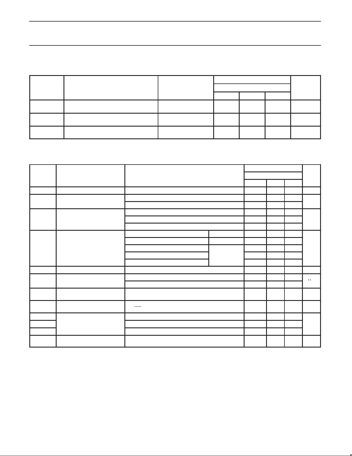
DC ELECTRICAL CHARACTERISTICS (2.5V 0.2V RANGE)
SYMBOL PARAMETER TEST CONDITIONS Temp = -40°C to +85°C UNIT
V
V
I
I
OFF
HOLD
I
EX
I
PU/PD
I
CCH
I
CCL
I
CCZ
∆I
NOTES:
1. All typical values are at V
2. This is the increase in supply current for each input at the specified voltage level other than V
3. This parameter is valid for any V
transition time of 100µsec is permitted. This parameter is valid for T
4. Unused pins at V
5. I
CCZ
6. Not guaranteed.
Input clamp voltage VCC = 2.3V; IIK = –18mA –0.85 –1.2 V
IK
p
Low-level output voltage
OL
Input leakage current
I
Off current VCC = 0V; VI or VO = 0 to 4.5V 0.1 ±100 µA
Bus Hold current VCC = 2.3V; VI = 0.7V 90
Data inputs
6
Current into an output in the
High state when V
Power up/down 3-State output
3
current
O
> V
CC
Quiescent supply current VCC = 2.7V; Outputs Low, VI = GND or V
Additional supply current per
CC
is measured with outputs pulled up to VCC or pulled down to ground.
input pin
2
or GND.
CC
= 2.5V and T
CC
CC
amb
between 0V and 1.2V with a transition time of up to 10msec. From V
= –40°C to +85°C.
amb
LIMITS
1.5
1.5
2.1
1.7
3.4
2.8
1
MAX
2.4
2.4
3.5
2.9
4.5
3.7
ns
ns
ns
MIN TYP
1
2
2
0.5
0.5
1.0
1.0
1.5
1.5
= 25°C.
LIMITS
MIN TYP1MAX
VCC = 2.3 to 3.6V; IOH = –100µA VCC–0.2
VCC = 2.3V; IOH = –8mA 1.8 2.1
VCC = 2.3V; IOL = 100µA 0.07 0.2
VCC = 2.3V; IOL = 24mA 0.3 0.5
VCC = 2.3V; IOL = 8mA 0.4
VCC = 2.7V; VI = V
or GND Control pins 0.1 ±1
CC
VCC = 0 or 2.7V; VI = 5.5V 0.1 10
VCC = 2.7V; VI = 5.5V
VCC = 2.7V; VI = V
CC
Data pins
0.1 20
0.1 10
µA
VCC = 2.7V; VI = 0 0.1 -5
VCC = 2.3V; VI = 1.7V –10
VO = 5.5V; VCC = 2.3V 50 125 µA
VCC ≤ 1.2V; VO = 0.5V to VCC; VI = GND or VCC;
OE/OE
= Don’t care
VCC = 2.7V; Outputs High, VI = GND or V
VCC = 2.7V; Outputs Disabled; VI = GND or V
CC,
CC,
I
O
I
O
CC,
VCC = 2.3V to 2.7V; One input at VCC–0.6V,
Other inputs at VCC or GND
= 0 0.04 0.1
= 0 2.3 45 mA
5
I
= 0
O
40 100 µA
0.04 0.1
0.1 0.4 mA
= 25°C.
or GND
= 25°C only.
amb
CC
= 1.2V to VCC = 2.5V ± 0.3V a
CC
V
1998 Feb 13
5
Page 6
Philips Semiconductors Product specification
74ALVT162452.5V/3.3V 16-bit transceiver (3-State)
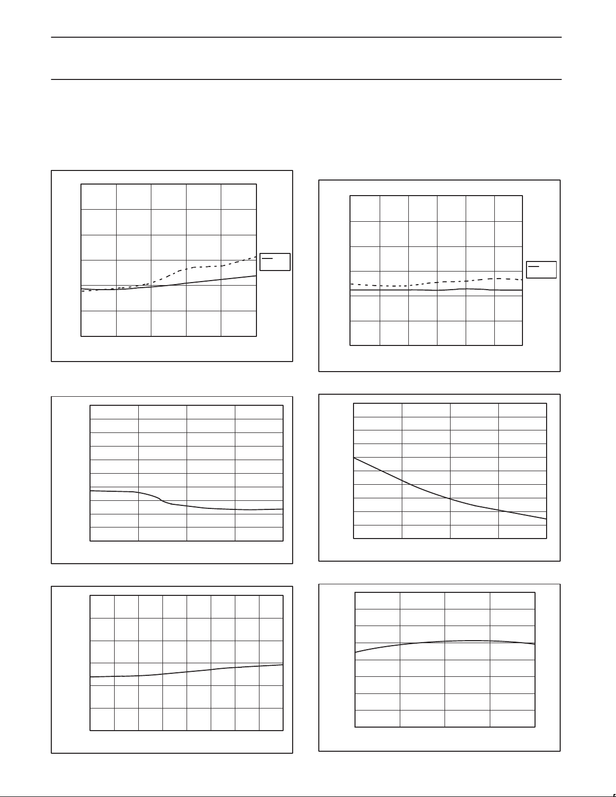
DYNAMIC SWITCHING THRESHOLD
Dynamic switching threshold is the change in VIH and VIL when the device is operated in various switching and output loading conditions. The
cause of this variation is due to extra load placed on internal circuit structures. V
V
is the input high switching level when the device is heavily loaded. V
IHD
V
ILD/VIHD
3.0
2.5
2.0
1.5
1.0
0.5
Input Dynamic Threshold Voltage (V)
0.0
2.3
vs V
CC
Vild/Vihd vs V
2.5 2.7 3.0 3.3 3.6
VCC (V)
CC
Vild
- - - - Vihd
SA00455
ILD
GROUND/VCC BOUNCE
V
vs Temperature
OLP
2.0
1.8
1.6
1.4
1.2
(V)
1.0
OLP
V
0.8
0.6
0.4
0.2
0.0
–55 –40 25 85 125
Temperature (°C)
SA00457
IHD
and V
are measures of the dynamic switching threshold.
ILD
is the input low switching level when the device is heavily loaded.
V
ILD/VIHD
vs Frequency
Temp = 25°C
3.00
2.50
2.00
1.50
1.00
Input Dynamic Threshold Voltage (V)
0.50
0.00
5 20 40 60 80 100 120
V
vs Capacitive Load
OLP
1.0
0.9
0.8
0.7
0.6
(V)
0.5
OLP
0.4
V
0.3
0.2
0.1
0.0
50pF
Vild/Vihd vs Frequency – T = 25°C
Frequency (MHz)
150pF
Capacitive Load (pF)
- - - - Vihd
SA00456
270pF
SA00459
Vild
V
vs Temperature
OHV
4.0
3.5
3.0
(V)
2.5
OHV
V
2.0
1.5
1.0
–55 –40 25 85 125
1998 Feb 13
Temperature (°C)
SA00458
V
vs Capacitive Load
OHV
4.0
3.5
3.0
2.5
(V)
2.0
OHV
V
1.5
1.0
0.5
0.0
50pF
Capacitive Load (pF)
150pF 270pF
SA00460
6
Page 7
Philips Semiconductors Product specification
s
s
74ALVT162452.5V/3.3V 16-bit transceiver (3-State)
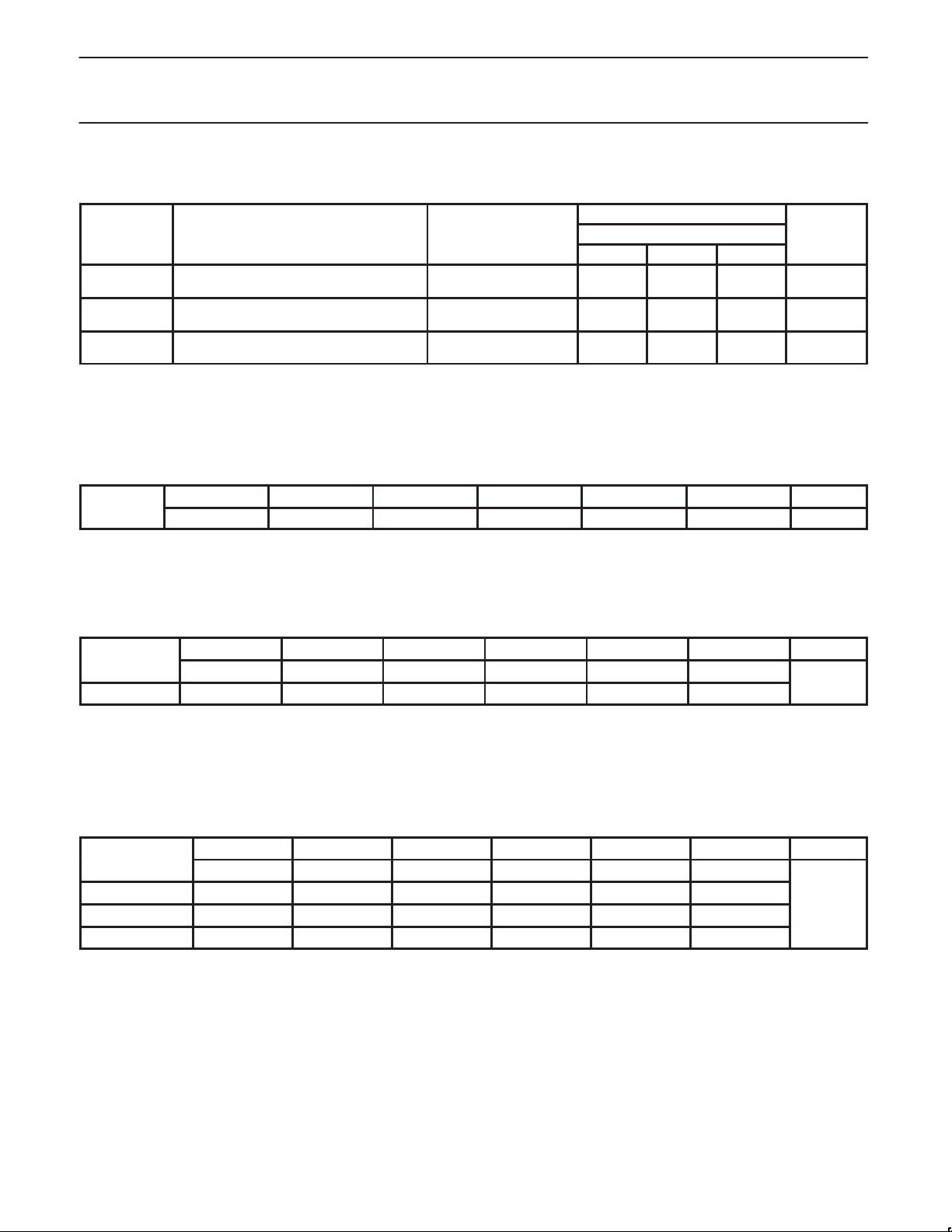
AC CHARACTERISTICS (2.5V 0.2V RANGE)
GND = 0V; tR = tF = 2.5ns; CL = 50pF; RL = 500Ω; T
SYMBOL PARAMETER WAVEFORM VCC = 2.5V 0.2V UNIT
t
PLH
t
PHL
t
PZH
t
PZL
t
PHZ
t
PLZ
Propagation delay
nAx to nBx or nBx to nAx
Output enable time
to High and Low level
Output disable time
from High and Low Level
NOTE:
1. All typical values are at V
= 2.5V and T
CC
amb
SKEW DATA
tps (Pin Skew or Transition Skew)
t
= | t
– t
PS
t
PS Max
PHL
|
PLH
VCC = 2.3 VCC = 2.5 VCC = 2.7 VCC = 3.0 VCC = 3.3 VCC = 3.6 UNITS
429 469 430 426 267 336 ps
= –40°C to +85°C.
amb
= 25°C.
LIMITS
1.7
1.9
3.0
2.3
3.0
2.3
1
MAX
2.8
2.8
4.5
3.5
4.6
3.5
ns
ns
ns
MIN TYP
1
2
2
0.5
0.5
1.5
1.0
1.5
1.0
t
OST
= | t
Pm
– t
Pn
|
Where is any edge transition (high-to-low or low-to-high)
measured between any two outputs (m or n) within any given
device.
VCC = 2.3 VCC = 2.5 VCC = 2.7 VCC = 3.0 VCC = 3.3 VCC = 3.6 UNITS
t
nAn-nBn
OST
546 625 586 546 427 397
nBn-nAn 508 547 586 506 427 417
NOTE:
One output switching, Temp = 25°C.
t
, t
OSHL
t
OSHL
t
OSLH
, (Common Edge Skew)
OSLH
= | t
= | t
PHL max
PLH max
– t
– t
| (Output Skew for Low-to-High Transitions)
PHL min
| (Output Skew for High-to-Low Transitions)
PLH min
VCC = 2.3 VCC = 2.5 VCC = 2.7 VCC = 3.0 VCC = 3.3 VCC = 3.6 UNITS
t
OSLH
t
OSHL
t
OSLH
t
OSHL
nAn-nBn
nAn-nBn
nBn-nAn
nBn-nAn
312 312 313 276 267 257
312 352 352 297 289 267
235 273 312 274 296 326
234 235 274 248 287 267
NOTE:
One output switching, Temp = 25°C.
p
p
1998 Feb 13
7
Page 8
Philips Semiconductors Product specification
74ALVT162452.5V/3.3V 16-bit transceiver (3-State)
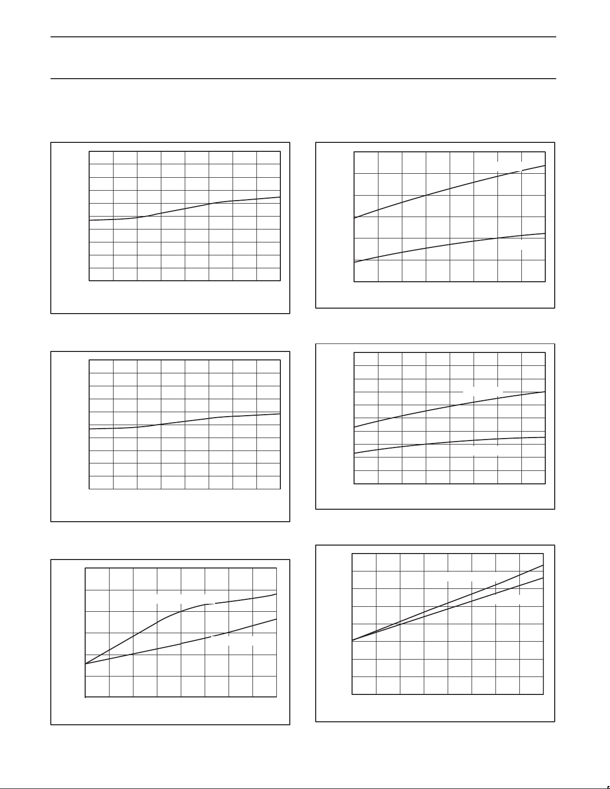
EXTENDED DATA
TPHL vs TEMP
VCC = 3.3V, one output switching
2.00
1.90
1.80
1.70
1.60
1.50
TPHL (nS)
1.40
1.30
1.20
1.10
1.00
–55 –40 25 85 125
Temperature (°C)
SA00449
TPLH vs NUMBER of OUTPUTS SWITCHING
T = 25°C, 50pF/500 ohm load
4.00
3.50
3.00
2.50
TPLH (nS)
2.00
1.50
1.00
1816
Number of Outputs Switching
VCC = 2.3V
VCC = 3.6V
SA00452
TPLH vs TEMP
VCC = 3.3V, one output switching
2.00
1.90
1.80
1.70
1.60
1.50
1.40
TPLH (nS)
1.30
1.20
1.10
1.00
–55 –40 25 85 125
Temperature (°C)
TPLH vs OUTPUT LOAD
Outputs also loaded with 500 ohms to ground, T= 25°C
6.00
5.00
4.00
3.00
TPLH (nS)
2.00
16 Outputs Switching
1 Output Switching
SA00450
TPHL vs NUMBER of OUTPUTS SWITCHING
T = 25°C, 50pF/500 ohm load
3.00
2.80
2.60
2.40
2.20
2.00
1.80
TPHL (nS)
1.60
1.40
1.20
1.00
1816
VCC = 2.3V
VCC = 3.6V
Number of Outputs Switching
TPHL vs OUTPUT LOAD
Outputs also loaded with 500 ohms to ground, T= 25°C
4.00
3.50
3.00
2.50
2.00
TPHL (nS)
1.50
1.00
16 Outputs Swicthing
1 Output Switching
SA00453
1.00
0.00
50pF 150pF 270pF
Capacitive Load (F)
1998 Feb 13
SA00451
0.50
0.00
50pF
150pF
Capacitive Load (pF)
270pF
SA00454
8
Page 9
Philips Semiconductors Product specification
74ALVT162452.5V/3.3V 16-bit transceiver (3-State)
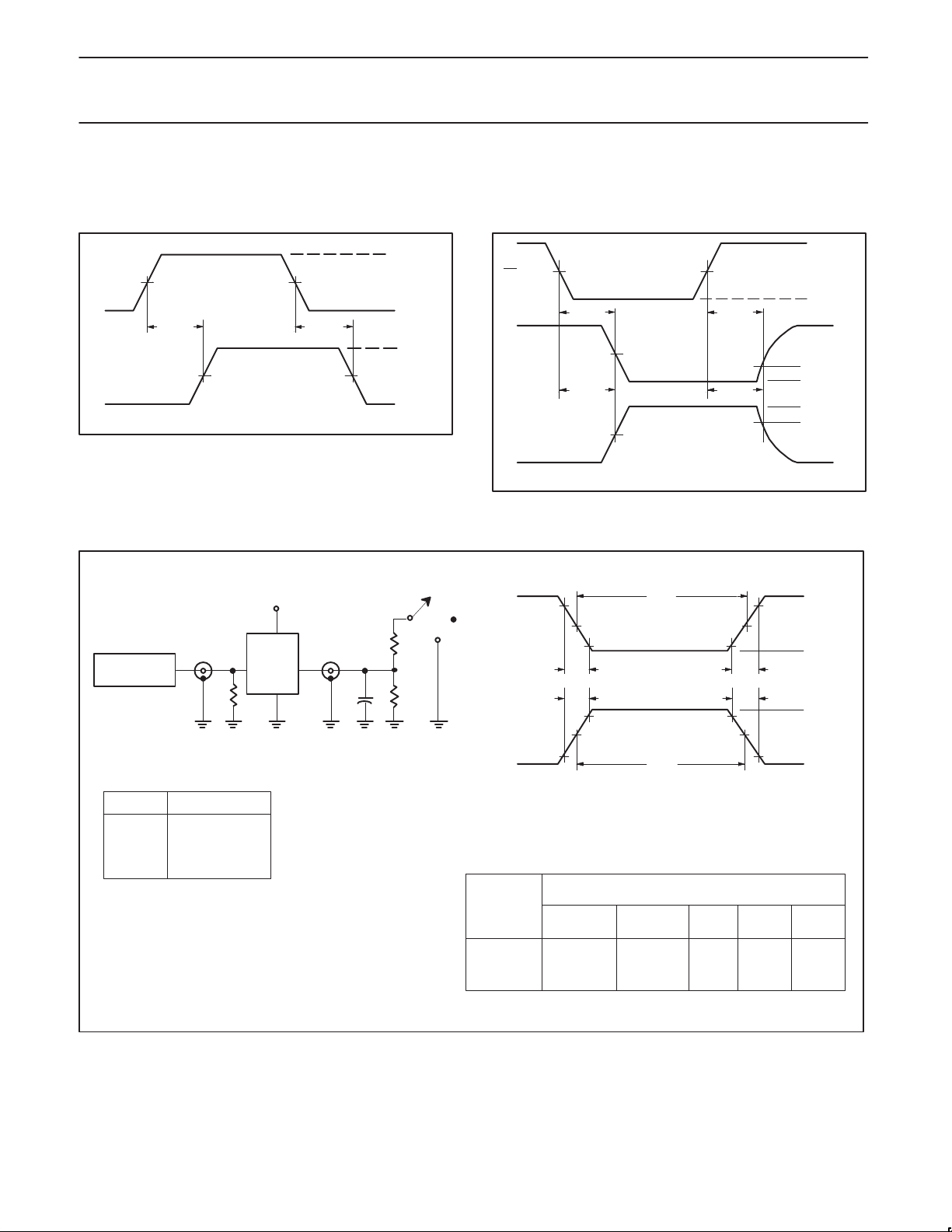
AC WAVEFORMS
VM = 1.5V at VCC w 3.0V, VM = VCC/2 at VCC v 2.7V
V
= VOL + 0.3V at VCC w 3.0V, VX = VOL + 0.15V at VCC v 2.7V
X
= VOH – 0.3V at VCC w 3.0V, VY = VOH – 0.15V at V
V
Y
An or Bn
INPUT
Bn or An
OUTPUT
V
M
t
PLH
V
M
VM = 1.5V or VCC/2, whichever is less
V
M
t
PHL
Waveform 1. Input to Output Propagation Delays
v 2.7V
CC
3.0V or V
whichever
is less
0V
V
OH
1.5V or VCC/2
V
OL
SW00023
3.0V or V
CC
CC
OE INPUT
OUTPUT
OUTPUT
V
M
t
PZL
V
M
t
PZH
V
M
V
M
t
PLZ
t
PHZ
whichever
is less
0V
V
X
V
OL
V
OH
V
Y
SW00024
6.0V or
V
x 2
CC
0V
Waveform 2. 3-State Output Enable and Disable Times
TEST CIRCUIT AND WAVEFORMS
V
CC
PULSE
GENERATOR
V
IN
D.U.T.
R
T
V
OUT
C
L
Test Circuit for 3-State Outputs
SWITCH POSITION
TEST SWITCH
t
PLZ/tPZL
t
PLH/tPHL
t
PHZ/tPZH
6V or V
Open
GND
CC x 2
DEFINITIONS
RL = Load resistor; see AC CHARACTERISTICS for value.
= Load capacitance includes jig and probe capacitance:
C
L
See AC CHARACTERISTICS for value.
R
= Termination resistance should be equal to Z
T
pulse generators.
OUT
R
R
of
L
L
6.0V or VCC x 2
Open
GND
FAMILY
74ALVT16
90%
NEGATIVE
PULSE
POSITIVE
PULSE
10%
t
W
V
M
10% 10%
t
(tF)
THL
t
(tR)t
TLH
90% 90%
V
M
t
W
INPUT PULSE REQUIREMENTS
Amplitude Rep. Rate t
3.0V or V
whichever
CC
v10MHz 500ns
is less
V
M
V
M
W
v2.5ns v2.5ns
90%
10%
t
R
t
TLH
THL
V
IN
0V
(tR)
(tF)
V
IN
0V
t
F
SW00025
1998 Feb 13
9
Page 10
Philips Semiconductors Product specification
74ALVT162452.5V/3.3V ALVT 16-bit transceiver (3-State)
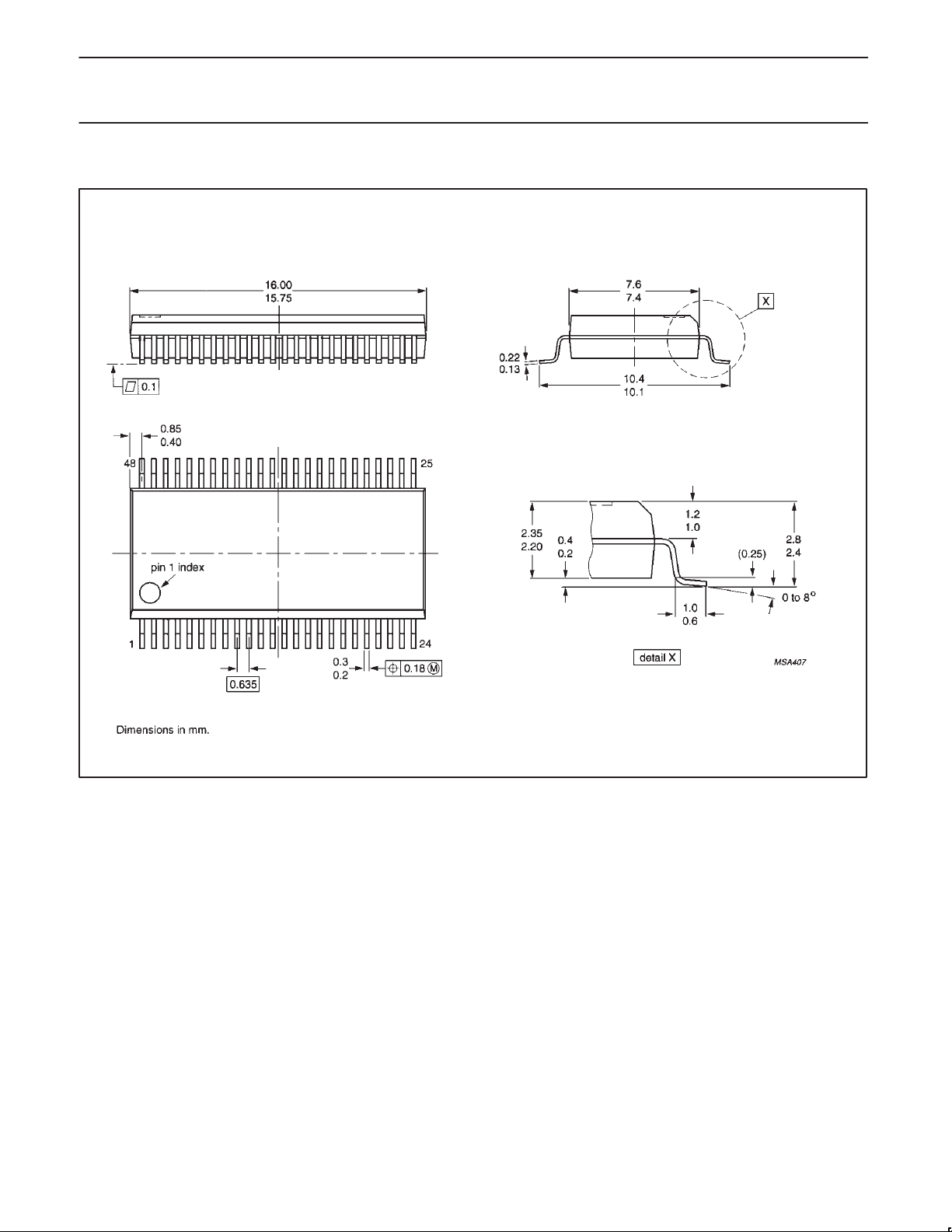
SSOP48: plastic shrink small outline package; 48 leads; body width 7.5mm SOT370-1
1998 Feb 13
10
Page 11
Philips Semiconductors Product specification
74ALVT162452.5V/3.3V ALVT 16-bit transceiver (3-State)
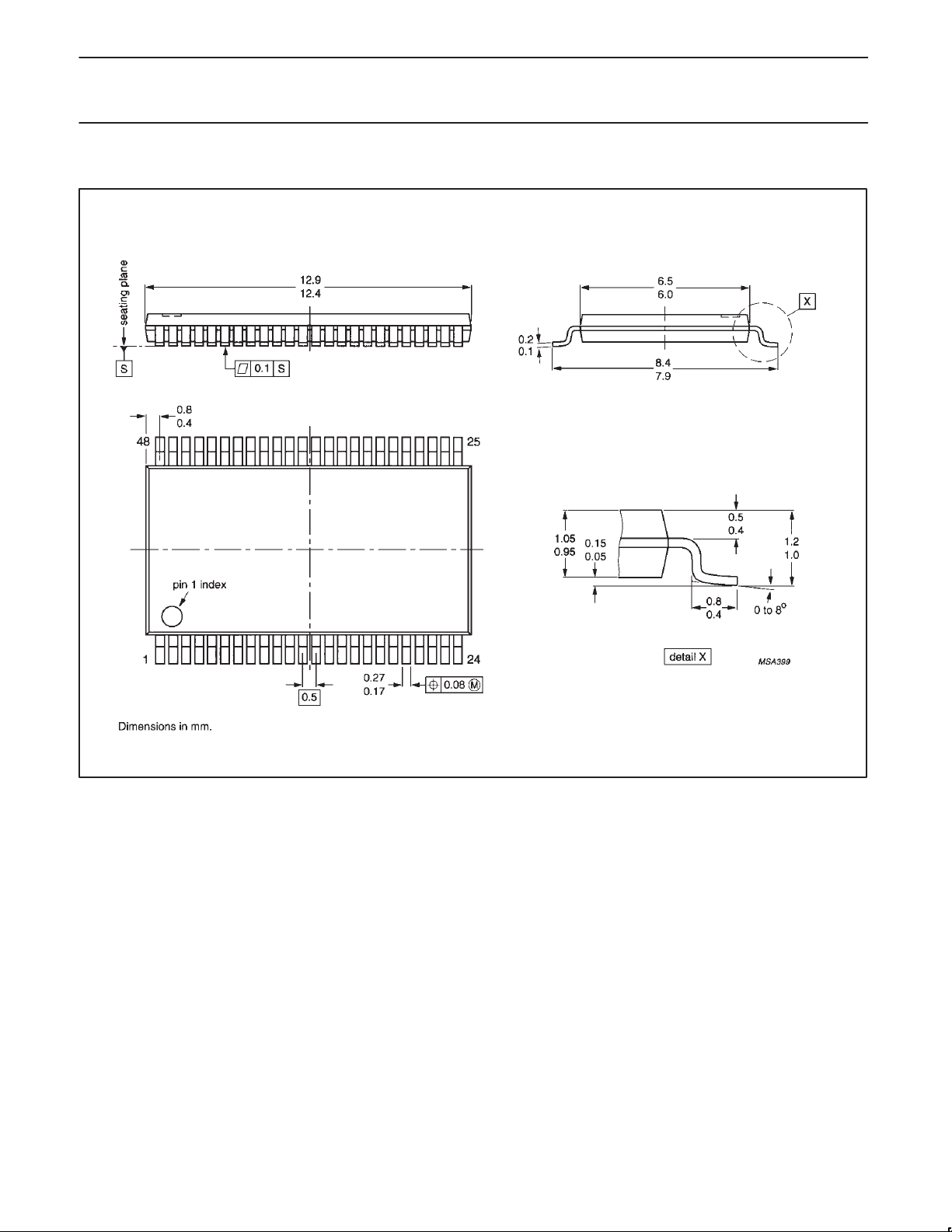
TSSOP48: plastic thin shrink small outline package; 48 leads; body width 6.1mm SOT362-1
1998 Feb 13
11
Page 12

Philips Semiconductors Product specification
74ALVT162452.5V/3.3V ALVT 16-bit transceiver (3-State)
Data sheet status
Data sheet
status
Objective
specification
Preliminary
specification
Product
specification
Product
status
Development
Qualification
Production
Definition
This data sheet contains the design target or goal specifications for product development.
Specification may change in any manner without notice.
This data sheet contains preliminary data, and supplementary data will be published at a later date.
Philips Semiconductors reserves the right to make chages at any time without notice in order to
improve design and supply the best possible product.
This data sheet contains final specifications. Philips Semiconductors reserves the right to make
changes at any time without notice in order to improve design and supply the best possible product.
[1]
[1] Please consult the most recently issued datasheet before initiating or completing a design.
Definitions
Short-form specification — The data in a short-form specification is extracted from a full data sheet with the same type number and title. For
detailed information see the relevant data sheet or data handbook.
Limiting values definition — Limiting values given are in accordance with the Absolute Maximum Rating System (IEC 134). Stress above one
or more of the limiting values may cause permanent damage to the device. These are stress ratings only and operation of the device at these or
at any other conditions above those given in the Characteristics sections of the specification is not implied. Exposure to limiting values for extended
periods may affect device reliability.
Application information — Applications that are described herein for any of these products are for illustrative purposes only. Philips
Semiconductors make no representation or warranty that such applications will be suitable for the specified use without further testing or
modification.
Disclaimers
Life support — These products are not designed for use in life support appliances, devices or systems where malfunction of these products can
reasonably be expected to result in personal injury . Philips Semiconductors customers using or selling these products for use in such applications
do so at their own risk and agree to fully indemnify Philips Semiconductors for any damages resulting from such application.
Right to make changes — Philips Semiconductors reserves the right to make changes, without notice, in the products, including circuits, standard
cells, and/or software, described or contained herein in order to improve design and/or performance. Philips Semiconductors assumes no
responsibility or liability for the use of any of these products, conveys no license or title under any patent, copyright, or mask work right to these
products, and makes no representations or warranties that these products are free from patent, copyright, or mask work right infringement, unless
otherwise specified.
Philips Semiconductors
811 East Arques Avenue
P.O. Box 3409
Sunnyvale, California 94088–3409
Telephone 800-234-7381
Copyright Philips Electronics North America Corporation 1998
All rights reserved. Printed in U.S.A.
print code Date of release: 05-96
Document order number: 9397-750-03647
yyyy mmm dd
12
 Loading...