

Page 1
74ALVC16721
Low Voltage 20-Bit D-Type Flip-Flops
with 3.6V Tolerant Inputs and Outputs
74ALVC16721 Low Voltage 20-Bit D-Type Flip-Flops with 3.6V Tolerant Inputs and Outputs
October 2001
Revised October 2001
General Description
The ALVC16721 contains twenty non-inverting D-type
flip-flops with 3-STATE outputs and is intended for bus oriented applications.
The 74ALVC16721 is designed for low voltage (1.65V to
3.6V) V
The 74ALVC16721 is fabricated w ith an advanc ed CMOS
technology to achieve high speed operation while maintaining low CMOS power dissipation.
applications with I/O compatibility up to 3.6V.
CC
Features
■ 1.8V–3.6V VCC supply operation
■ 3.6V tolerant inputs and outputs
(CLK to On)
■ t
PD
4.0 ns max for 3.0V to 3.6V V
4.9 ns max for 2.3V to 2.7V V
8.8 ns max for 1.65V to 1.95V V
■ Power-off high impedance inputs and outputs
■ Supports live insertion and withdrawal (Note 1)
■ Uses patented noise/EMI reductio n circuitr y
■ Latchup conforms to JEDEC JED78
■ ESD performance:
Human body model
Machine model
Note 1: To ensure the high-impedance state d uring power up or power
down, OE
should be tied to VCC through a pull-up r esistor; the min imum
value of the res istor is d eter mine d by the cu rre nt-sou rcin g ca pa bility of t he
driver.
> 200V
CC
CC
CC
> 2000V
Ordering Code:
Order Number Package Number Package Description
74ALVC16721MTD MTD56 56-Lead Thin Shrink Small Outline Package (TSSOP), JEDEC MO-153, 6.1mm Wide
Device also available in Tape and Reel. Specify by appending suffix letter “X” to the ordering co de.
Logic Symbol Pin Descriptions
Pin Names Description
OE
CLK Clock Input
D
0–D19
O
0–O19
CE
Output Enable Input (Active LOW)
Inputs
Outputs
Clock Enable Input (Active LOW)
© 2001 Fairchild Semiconductor Corporation DS500691 www.fairchildsemi.com
Page 2
Connection Diagram Truth Table
74ALVC16721
Logic Diagram
CLK CE OE
D0–D
O0–O
19
19
XXH X Z
XHL X O
LL L L
LL H H
L or H L L X O
H = HIGH Voltage Level
L = LOW Voltage Level
X = Immaterial (HIGH or LOW, inputs may not float)
Z = High Impedance
O0 = Previous O0 before L O W-to-HIGH tran sition of Clock
= LOW-to-HIGH transition
0
0
Functional Description
The 74ALVC16721 contains twenty D-type flip-fl ops with
3-STATE standard outputs. The twenty flip-flops will store
the state of their individual D-type inputs that meet the
setup and hold time requirements on the LOW-HIGH Clock
(CLK) transition, whe n the Clock-Enable (CE
3-STATE standard outputs are controlled by the Output
Enable (OE
). When OE is HIGH , the st andard ou tputs are
in high impedance m ode but this does not interfere with
entering new data into the flip-flops.
) is LOW. The
www.fairchildsemi.com 2
Page 3
Absolute Maximum Ratings(Note 2) Recommended Operating
Supply Voltage (VCC) −0.5V to +4.6V
DC Input Voltage (V
Output Voltage (V
DC Input Diode Current (I
V
< 0V −50 mA
I
DC Output Diode Current (I
< 0V −50 mA
V
O
) −0.5V to 4.6V
I
) (Note 3) −0.5V to VCC +0.5V
O
)
IK
)
OK
DC Output Source/Sink Current
(I
) ±50 mA
OH/IOL
or GND Current per
DC V
CC
Supply Pin (I
Storage Temperature Range (T
or GND) ±100 mA
CC
) −65°C to +150°C
STG
Conditions
Power Supply
Operating 1.65V to 3.6V
Input Voltage (V
Output Voltage (VO)0V to V
Free Air Operating Temperature (TA) −40°C to +85°C
Minimum Input Edge Rate (
= 0.8V to 2.0V, VCC = 3.0V 10 ns/V
V
IN
Note 2: The Absolute Maxi mum Ratings are thos e values beyond which
the safety of the d evice cannot b e guaranteed . The device sh ould not be
operated at these limit s. The parametric values defi ned in the Electrical
Characteristics tables are not guaranteed at the Absolute Maximum Ratings. The “Recommended Operating Conditions” table will define the conditions for actual device operation.
Absolute Maximum Rating must be observed.
Note 3: I
O
Note 4: Floating or unused inputs must be held HIGH or LOW.
(Note 4)
)0V to V
I
∆t/∆V)
DC Electrical Characteristics
V
Symbol Parameter Conditions
V
IH
V
IL
V
OH
V
OL
I
I
I
OZ
I
CC
∆I
HIGH Level Input Voltage 1.65 -1.95 0.65 x V
LOW Level Input Voltage 1.65 -1.95 0.35 x V
HIGH Level Output Voltage IOH = −100 µA 1.65 - 3.6 VCC - 0.2
LOW Level Output Voltage IOL = 100 µA 1.65 - 3.6 0.2
Input Leakage Current 0 ≤ VI ≤ 3.6V 3.6 ±5.0 µA
3-STATE Output Leakage 0 ≤ VO ≤ 3.6V 3.6 ±10 µA
Quiescent Supply Current VI = VCC or GND, IO = 0 3.6 40 µA
Increase in ICC per Input VIH = VCC − 0.6V 3 -3.6 750 µA
CC
IOH = −4 mA 1.65 1.2
I
= −6 mA 2.3 2
OH
= −12 mA 2.3 1.7
I
OH
IOH = −24 mA 3.0 2
I
= 4 mA 1.65 0.45
OL
= 6 mA 2.3 0.4
I
OL
IOL = 12mA 2.3 0.7
IOL = 24 mA 3 0.55
CC
(V)
2.7 - 3.6 2.0
2.7 - 3.6 0.8
2.7 2.2
3.0 2.4
2.7 0.4
Min Max Units
CC
74ALVC16721
CC
CC
V2.3 - 2.7 1.7
CC
V2.3 - 2.7 0.7
V
V
3 www.fairchildsemi.com
Page 4
AC Electrical Characteristics
T A = −40°C to +85°C, RL = 500Ω
Symbol Parameter
V
CC
CL = 50 pF CL = 30 pF
= 3.3V ± 0.3V V
= 2.7V V
CC
MinMaxMinMaxMinMaxMinMax
74ALVC16721
f
t
t
t
t
t
t
MAX
PHL
PZL
PLZ
W
S
H
Maximum Clock Frequency 250 200 200 100 ns
, t
Propagation Delay
PLH
Bus to Bus
, t
Output Enable Time 1.3 4.3 1.5 5.4 1.0 4.9 1.5 9.8 ns
PZH
, t
Output Disable Time 1.3 4.2 1.5 4.7 1.0 4.2 1.5 7.6 ns
PHZ
1.3 4 .0 1.5 4.9 1.0 4.4 1.5 8.8 ns
Pulse Width 1.5 1.5 1.5 4.0 ns
Setup Time 1.5 1.5 1.5 2.5 ns
Hold Time 1.0 1.0 1.0 1.0 ns
Capacitance
Symbol Parameter Conditions
C
IN
C
OUT
C
PD
Input Capacitance VI = 0V or V
Output Capacitance VI = 0V or V
CC
CC
Power Dissipation Capacitance Outputs Enabled f = 10 MHz, CL = 50 pF 3.3 20
= 2.5V ± 0.2V V
CC
= 1.8V ± 0.15V
CC
T
= +25°C
A
V
Typical
CC
Units
3.3 6 pF
3.3 7 pF
2.5 20
Units
pF
www.fairchildsemi.com 4
Page 5
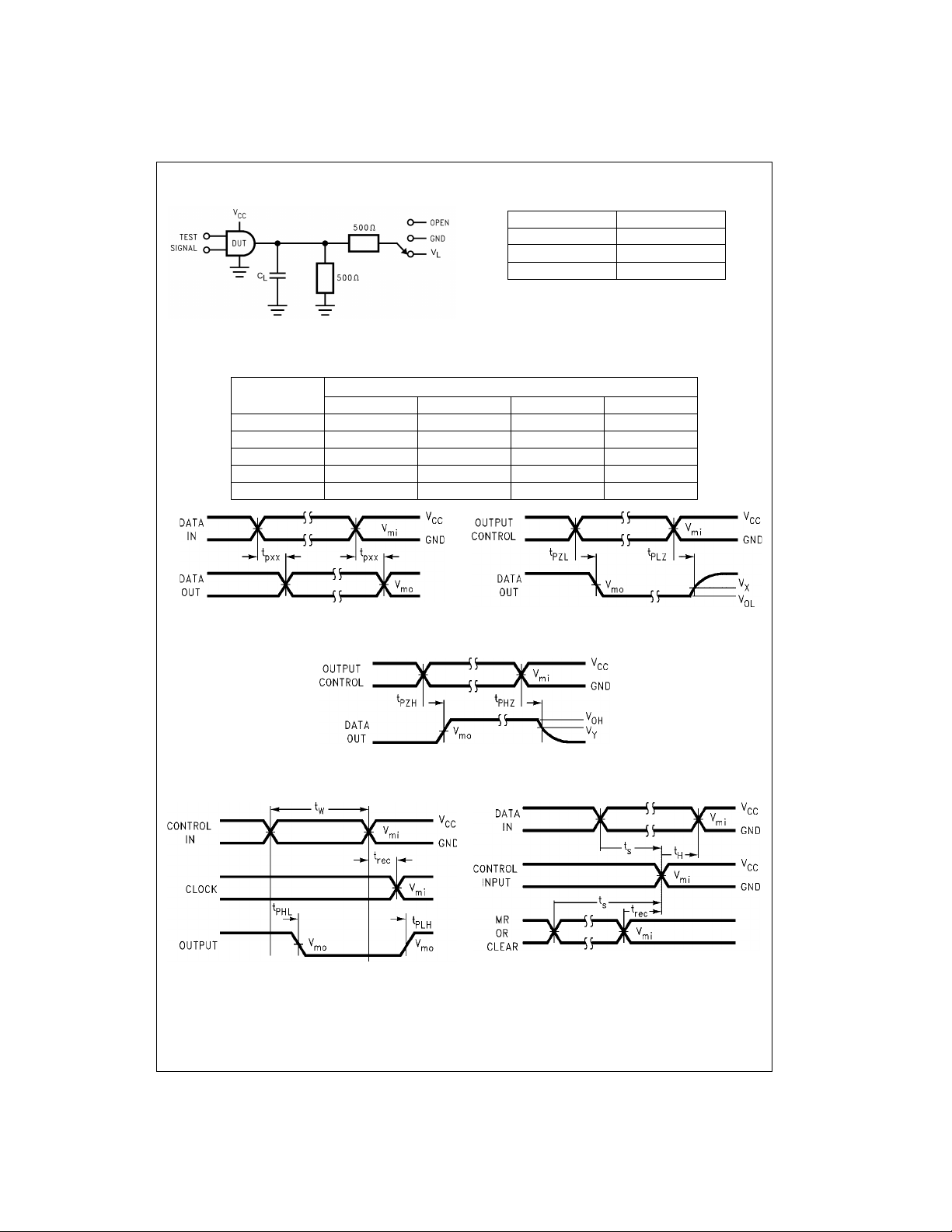
AC Loading and Waveforms
FIGURE 1. AC Test Circuit
(Input Characteristics: f
Symbol
V
mi
V
mo
V
X
V
Y
V
L
3.3V ± 0.3V 2.7V 2.5V ± 0.2V 1.8V ± 0.1 5V
1.5V 1.5V VCC/2 VCC/2
1.5V 1.5V VCC/2 VCC/2
VOL + 0.3V VOL + 0.3V VOL + 0.15V VOL + 0.15V
VOH − 0.3V VOH − 0.3V VOH − 0.15V VOH − 0.15V
6V 6V VCC*2 VCC*2
TABLE 2. Variable Matrix
= 1MHz; t
= tf = 2ns; Z0 = 50Ω)
r
V
CC
TABLE 1. Values for Figure 1
TEST SWITCH
t
t
t
PLH
PZL
PZH
, t
PHL
, t
PLZ
, t
PHZ
Open
V
GND
L
74ALVC16721
FIGURE 2. Waveform for Inverting
and Non-inverting Functions
FIGURE 4. 3-STATE Output High Enable
and Disable Times for Low Voltage Logic
FIGURE 5. Propagation Delay, Pulse Width
and t
Wav eforms
rec
FIGURE 3. 3-STATE Output Low Enable
and Disable Times for Low Voltage Logic
FIGURE 6. Setup Time, Hold Time and Recovery Time
for Low Voltage Logic
5 www.fairchildsemi.com
Page 6
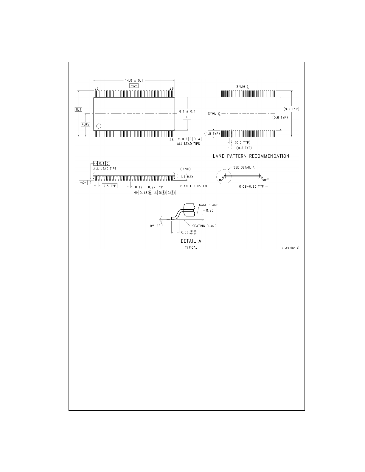
Physical Dimensions inches (millimeters) unless otherwise noted
56-Lead Thin Shrink Small Outline Package (TSSOP), JEDEC MO-153, 6.1mm Wide
Fairchild does not assume any responsibility for use of any circuitr y described, no circuit patent licenses are implied a nd
74ALVC16721 Low Voltage 20-Bit D-Type Flip-Flops with 3.6V Tolerant Inputs and Outputs
Fairchild reserves the right at any time without notice to change said circuitry and specifications.
LIFE SUPPORT POLICY
FAIRCHILD’S PRODUCTS ARE NOT AUTHORIZED FOR USE AS CRITICAL COMPONENTS IN LIFE SUPPORT
DEVICES OR SYSTEMS WITHOUT THE EXPRESS WRITTEN APPROVAL OF THE PRESIDENT OF FAIRCHILD
SEMICONDUCTOR CORPORATION. As used herein:
1. Life support de vices o r systems a re devices or syste ms
which, (a) are intended for surgical implant into the
body, or (b) support or sustain life, and (c) whose failure
to perform when properly used in accordance with
instructions for use provided in the labeling, can be reasonably expected to result in a significant inju ry to the
user.
www.fairchildsemi.com 6
Package Number MTD56
2. A critical com ponent in any com ponen t of a life su pport
device or system whose failu re to perform can be reasonably expected to cause the failure of the li fe su pp ort
device or system, or to affect its safety or effectiveness.
www.fairchildsemi.com
 Loading...