

Page 1

查询74ALVC14BQ供应商
74ALVC14
Hex inverting Schmitt trigger
Rev. 03 — 15 February 2005 Product data sheet
1. General description
The 74ALVC14 is a high-performance, low-power, low-voltage, Si-gate CMOS device and
superior to most advanced CMOS compatible TTL families.
The 74ALVC14 provides six inverting buffers with Schmitt-trigger action. It is capable of
transforming slowly changing input signals into sharply defined, jitter-free output signals.
2. Features
■ Wide supply voltage range from 1.65 V to 3.6 V
■ 3.6 V tolerant inputs/outputs
■ CMOS low power consumption
■ Direct interface with TTL levels (2.7 V to 3.6 V)
■ Power-down mode
■ Unlimited input rise and fall times
■ Latch-up performance exceeds 250 mA
■ Complies with JEDEC standard:
◆ JESD8-7 (1.65 V to 1.95 V)
◆ JESD8-5 (2.3 V to 2.7 V)
◆ JESD8-B/JESD36 (2.7 V to 3.6 V)
■ ESD protection:
◆ HBM EIA/JESD22-A114-B exceeds 2000 V
◆ MM EIA/JESD22-A115-A exceeds 200 V
■ Multiple package options
3. Quick reference data
Table 1: Quick reference data
Symbol Parameter Conditions Min Typ Max Unit
, t
t
PHL
propagation delay nA
PLH
to nY
VCC= 1.8 V; CL= 30 pF;
R
= 1 kΩ
L
= 2.5 V; CL= 30 pF;
V
CC
R
= 500 Ω
L
= 2.7 V; CL= 50 pF;
V
CC
R
= 500 Ω
L
= 3.3 V; CL= 50 pF;
V
CC
R
= 500 Ω
L
- 2.9 - ns
- 2.2 - ns
- 2.8 - ns
- 2.4 - ns
Page 2

Philips Semiconductors
74ALVC14
Hex inverting Schmitt trigger
Table 1: Quick reference data
…continued
Symbol Parameter Conditions Min Typ Max Unit
C
I
C
PD
input capacitance - 3.5 - pF
power dissipation
VCC = 3.3 V
[1] [2]
-25-pF
capacitance per buffer
[1] CPD is used to determine the dynamic power dissipation (PD in µW).
PD = CPD× V
fi = input frequency in MHz;
fo = output frequency in MHz;
CL = output load capacitance in pF;
VCC = supply voltage in V;
N = number of inputs switching;
Σ(CL× V
[2] The condition is VI = GND to VCC.
2
× fi× N + Σ(CL× V
CC
2
× fo) = sum of the outputs.
CC
2
× fo) where:
CC
4. Ordering information
Table 2: Ordering information
Type number Package
Temperature range Name Description Version
74ALVC14D −40 °C to +85 °C SO14 plastic small outline package; 14 leads;
body width 3.9 mm
74ALVC14PW −40 °C to +85 °C TSSOP14 plastic thin shrink small outline package; 14 leads;
body width 4.4 mm
74ALVC14BQ −40 °C to +85 °C DHVQFN14 plastic dual in-line compatible thermal enhanced very
thin quad flat package; no leads; 14 terminals;
body 2.5 × 3 × 0.85 mm
SOT108-1
SOT402-1
SOT762-1
9397 750 14592 © Koninklijke Philips Electronics N.V. 2005. All rights reserved.
Product data sheet Rev. 03 — 15 February 2005 2 of 16
Page 3

Philips Semiconductors
5. Functional diagram
74ALVC14
Hex inverting Schmitt trigger
1
1
3
5
9
11
13
1A 1Y
2A 2Y
3A 3Y
4A 4Y
5A 5Y
6A 6Y
mna204
2
4
6
8
10
12
3
5
9
11
13
001aac497
Fig 1. Logic symbol Fig 2. IEC logic symbol
A
Y
mna025
2
4
6
8
10
12
Fig 3. Logic diagram (one Schmitt trigger)
9397 750 14592 © Koninklijke Philips Electronics N.V. 2005. All rights reserved.
Product data sheet Rev. 03 — 15 February 2005 3 of 16
Page 4

Philips Semiconductors
6. Pinning information
6.1 Pinning
74ALVC14
Hex inverting Schmitt trigger
1
1A V
2
1Y 6A
3
2A 6Y
4
2Y 5A
5
3A 5Y
6
3Y 4A
7
GND 4Y
14
Fig 4. Pin configuration SO14 and
TSSOP14
6.2 Pin description
Table 3: Pin description
Symbol Pin Description
1A 1 1 data input A
1Y 2 1 data output Y
2A 3 2 data input A
2Y 4 2 data output Y
3A 5 3 data input A
3Y 6 3 data output Y
GND 7 ground (0 V)
4Y 8 4 data output Y
4A 9 4 data input A
5Y 10 5 data output Y
5A 11 5 data input A
6Y 12 6 data output Y
6A 13 6 data input A
V
CC
14 supply voltage
001aac498
GND
1A
1
14
(1)
7
GND
V
14
8
4Y
CC
001aac499
terminal 1
index area
2 13
1Y 6A
3 12
14
CC
13
12
11
10
9
8
2A 6Y
4 11
2Y 5A
5 10
3A 5Y
6 9
3Y 4A
Transparent top view
The die substrate is attached to the
exposed die pad using conductive die
attach material. It can not be used as
a supply pin or input.
Fig 5. Pin configuration DHVQFN14
9397 750 14592 © Koninklijke Philips Electronics N.V. 2005. All rights reserved.
Product data sheet Rev. 03 — 15 February 2005 4 of 16
Page 5

Philips Semiconductors
7. Functional description
7.1 Function table
74ALVC14
Hex inverting Schmitt trigger
Table 4: Function table
Input Output
nA nY
LH
HL
[1] H = HIGH voltage level;
L = LOW voltage level.
8. Limiting values
Table 5: Limiting values
In accordance with the Absolute Maximum Rating System (IEC 60134). Voltages are referenced to
GND (ground = 0 V).
Symbol Parameter Conditions Min Max Unit
V
CC
V
I
V
O
I
IK
I
OK
I
O
,
I
CC
I
GND
T
stg
P
tot
[1] The input and output voltage ratings may be exceeded if the input and output current ratings are observed.
[2] When VCC = 0 V (Power-down mode), the output voltage can be 3.6 V in normal operation.
[3] For SO14 packages: P
For TSSOP14 packages: P
For DHVQFN14 packages: P
[1]
supply voltage −0.5 +4.6 V
input voltage
output voltage Active mode
Power-down mode
[1]
−0.5 +4.6 V
[1]
−0.5 VCC + 0.5 V
[2]
−0.5 +4.6 V
input diode current VI < 0 V - −50 mA
output diode current VO > VCC or VO < 0 V - ±50 mA
output source or sink
VO = 0 V to V
CC
- ±50 mA
current
VCC or GND current - ±100 mA
storage temperature −65 +150 °C
total power dissipation T
derates linearly with 8 mW/K above 70 °C.
tot
derates linearly with 5.5 mW/K above 60 °C.
tot
derates linearly with 4.5 mW/K above 60 °C.
tot
= −40 °C to +85 °C
amb
[3]
- 500 mW
9397 750 14592 © Koninklijke Philips Electronics N.V. 2005. All rights reserved.
Product data sheet Rev. 03 — 15 February 2005 5 of 16
Page 6

Philips Semiconductors
74ALVC14
Hex inverting Schmitt trigger
9. Recommended operating conditions
Table 6: Recommended operating conditions
Symbol Parameter Conditions Min Typ Max Unit
V
CC
V
I
V
O
T
amb
supply voltage 1.65 - 3.6 V
input voltage 0 - 3.6 V
output voltage VCC = 1.65 V to 3.6 V 0 - V
Power-down mode;
= 0 V
V
CC
0 - 3.6 V
CC
V
ambient temperature −40 - +85 °C
10. Static characteristics
Table 7: Static characteristics
At recommended operating conditions; voltages are referenced to GND (ground = 0 V).
Symbol Parameter Conditions Min Typ Max Unit
= −40 °C to +85 °C
T
amb
V
V
I
I
I
∆I
OL
OH
LI
off
CC
CC
LOW-level output voltage VI = VIH or V
HIGH-level voltage output VI = VIH or V
input leakage current VCC = 3.6 V; VI = 3.6 V or GND - ±0.1 ±5 µA
power-off leakage current VCC = 0 V; VI or VO = 3.6 V - ±0.1 ±10 µA
quiescent supply current VCC= 3.6 V; VI=VCCor GND; IO= 0 A - 0.2 10 µA
additional quiescent supply
current per input pin
C
I
input capacitance - 3.5 - pF
[1]
IL
IO= 100 µA; VCC = 1.65 V to 3.6 V - - 0.2 V
= 6 mA; VCC = 1.65 V - 0.11 0.3 V
I
O
= 12 mA; VCC = 2.3 V - 0.17 0.4 V
I
O
= 18 mA; VCC = 2.3 V - 0.25 0.6 V
I
O
= 12 mA; VCC = 2.7 V; - 0.16 0.4 V
I
O
= 18 mA; VCC = 3.0 V - 0.23 0.4 V
I
O
= 24 mA; VCC = 3.0 V - 0.30 0.55 V
I
O
IL
IO= −100 µA; VCC = 1.65 V to 3.6 V VCC− 0.2 - - V
= −6 mA; VCC = 1.65 V 1.25 1.51 - V
I
O
= −12 mA; VCC = 2.3 V 1.8 2.10 - V
I
O
= −18 mA; VCC = 2.3 V 1.7 2.01 - V
I
O
= −12 mA; VCC = 2.7 V; 2.2 2.53 - V
I
O
= −18 mA; VCC = 3.0 V 2.4 2.76 - V
I
O
= −24 mA; VCC = 3.0 V 2.2 2.68 - V
I
O
VCC= 3.0 V to 3.6 V; VI=VCC− 0.6 V;
I
= 0 A
O
- 5 750 µA
[1] Typical values are measured at T
9397 750 14592 © Koninklijke Philips Electronics N.V. 2005. All rights reserved.
Product data sheet Rev. 03 — 15 February 2005 6 of 16
amb
= 25 °C.
Page 7
Philips Semiconductors
74ALVC14
Hex inverting Schmitt trigger
11. Dynamic characteristics
Table 8: Dynamic characteristics
Voltages are referenced to GND (ground = 0 V); for test circuit see Figure 7.
Symbol Parameter Conditions Min Typ Max Unit
= −40 °C to +85 °C
T
amb
t
,
PHL
t
PLH
C
PD
propagation delay nA to nY see Figure 6
power dissipation
capacitance per buffer
[1]
= 1.65 V to 1.95 V 1.0 2.9 4.4 ns
V
CC
= 1.95 V to 2.7 V 1.0 2.2 3.7 ns
V
CC
= 2.7 V 1.0 2.8 3.9 ns
V
CC
= 3.0 V to 3.6 V 1.0 2.4 3.4 ns
V
CC
VCC = 3.3 V
[2] [3]
-25-pF
[1] Typical values are measured at T
[2] CPD is used to determine the dynamic power dissipation (PD in µW).
PD = CPD× V
fi = input frequency in MHz;
fo = output frequency in MHz;
CL = output load capacitance in pF;
VCC = supply voltage in V;
N = number of inputs switching;
Σ(CL× V
[3] The condition is VI = GND to VCC.
2
× fi× N + Σ(CL× V
CC
2
× fo) = sum of the outputs.
CC
amb
CC
= 25 °C.
2
× fo) where:
12. Waveforms
V
I
nA input
GND
V
OH
nY output
V
OL
V
M
t
PHL
V
M
t
PLH
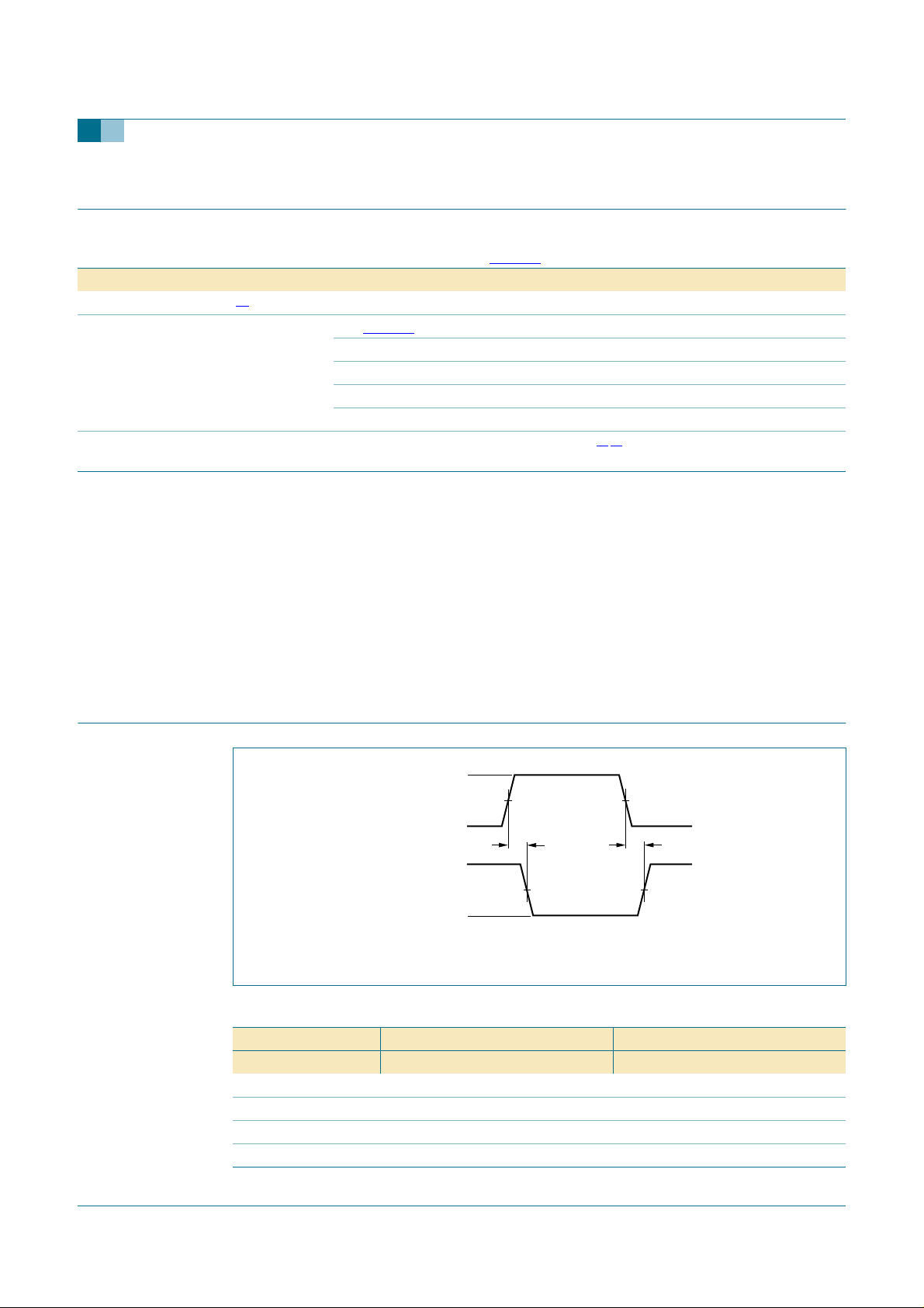
mna344
VOL and VOH are typical output voltage drop that occur with the output load.
Fig 6. Propagation delay input (nA) to output (nY)
Table 9: Measurement points
Supply Input Output
V
CC
1.65 V to 1.95 V 0.5 × V
2.3 V to 2.7 V 0.5 × V
V
M
CC
CC
V
M
0.5 × V
0.5 × V
CC
CC
2.7 V 1.5 V 1.5 V
3.0 V to 3.6 V 1.5 V 1.5 V
9397 750 14592 © Koninklijke Philips Electronics N.V. 2005. All rights reserved.
Product data sheet Rev. 03 — 15 February 2005 7 of 16
Page 8
Philips Semiconductors
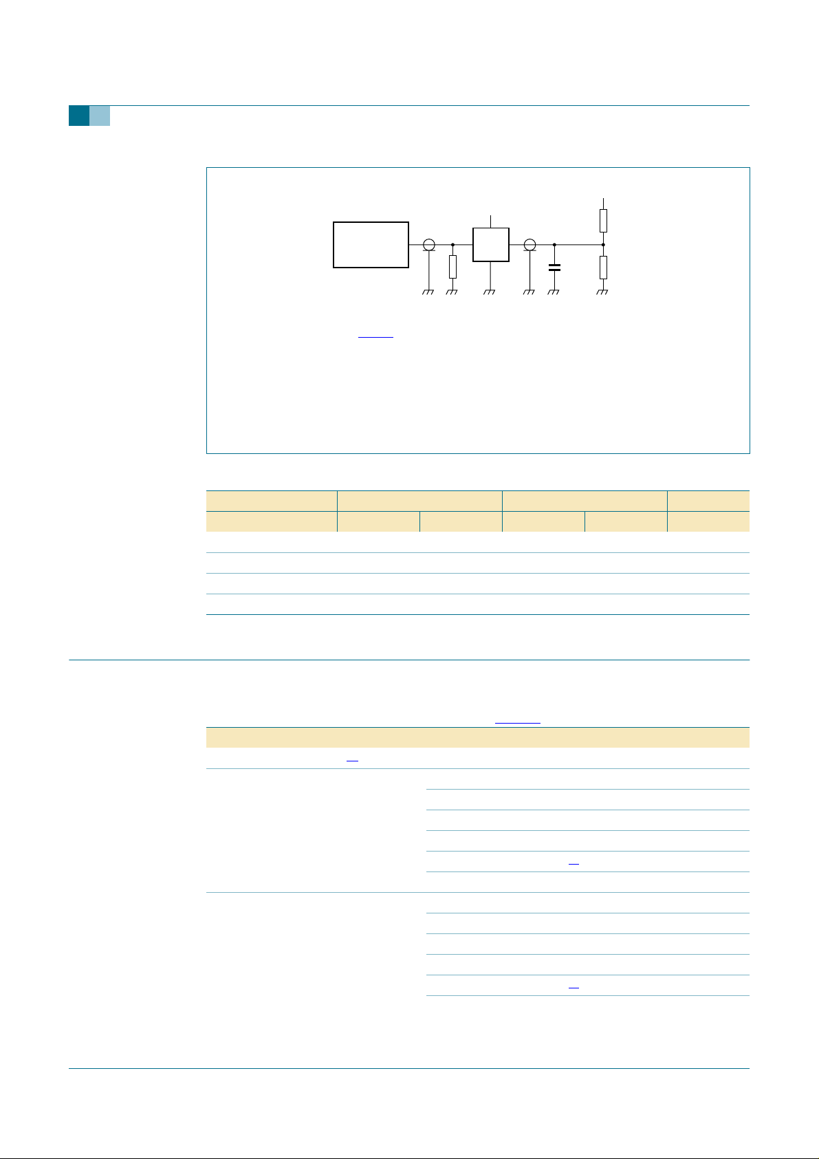
Fig 7. Load circuitry for switching times
Table 10: Test data
Supply Input Load V
V
CC
1.65 V to 1.95 V V
2.3 V to 2.7 V V
2.7 V 2.7 V ≤ 2.5 ns 50 pF 500 Ω open
3.0 V to 3.6 V 2.7 V ≤ 2.5 ns 50 pF 500 Ω open
74ALVC14
Hex inverting Schmitt trigger
V
EXT
V
CC
V
PULSE
GENERATOR
Test data is given in Table 9.
Definitions test circuit:
RT = Termination resistance should be equal to output impedance Zo of the pulse generator.
CL = Load capacitance including jig and probe capacitance.
RL = Load resistor.
V
= Test voltage for switching times.
EXT
V
I
CC
CC
I
tr, t
D.U.T.
R
T
f
≤ 2.0 ns 30 pF 1 kΩ open
≤ 2.0 ns 30 pF 500 Ω open
V
O
C
C
L
R
L
R
L
mna616
R
L
L
EXT
t
, t
PLH
PHL
13. Transfer characteristics
Table 11: Transfer characteristics
The VIH and VIL from the family static characteristics are superseded by the VT+ and V
Voltages are referenced to GND (ground = 0 V); see
Symbol Parameter Conditions Min Typ Max Unit
= −40 °C to +85 °C
T
amb
V
T+
V
T−
positive-going threshold VCC = 1.65 V 0.7 0.98 1.24 V
negative-going threshold VCC = 1.65 V 0.41 0.64 0.9 V
[1]
Figure 8.
= 1.95 V 0.75 1.12 1.46 V
V
CC
= 2.3 V 0.9 1.27 1.7 V
V
CC
= 2.7 V 1.0 1.43 2.0 V
V
CC
= 3.0 V
V
CC
= 3.6 V 1.1 1.81 2.0 V
V
CC
= 1.95 V 0.49 0.76 1.1 V
V
CC
= 2.3 V 0.6 0.90 1.3 V
V
CC
= 2.7 V 0.7 1.06 1.4 V
V
CC
= 3.0 V
V
CC
= 3.6 V 0.8 1.42 1.7 V
V
CC
[2]
1.1 1.56 2.0 V
[2]
0.8 1.19 1.5 V
.
T
−
9397 750 14592 © Koninklijke Philips Electronics N.V. 2005. All rights reserved.
Product data sheet Rev. 03 — 15 February 2005 8 of 16
Page 9
Philips Semiconductors
74ALVC14
Hex inverting Schmitt trigger
Table 11: Transfer characteristics
…continued
The VIH and VIL from the family static characteristics are superseded by the VT+ and V
Voltages are referenced to GND (ground = 0 V); see
Symbol Parameter Conditions Min Typ Max Unit
V
H
[1] All typical values are measured at T
[2] The typical transfer characteristic is displayed inFigure 9.
hysteresis (VT+− VT−)V
amb
14. Waveforms transfer characteristics
V
O
Figure 8.
= 1.65 V 0.25 0.34 0.62 V
CC
= 1.95 V 0.25 0.36 0.62 V
V
CC
= 2.3 V 0.3 0.36 1.0 V
V
CC
= 2.7 V 0.3 0.38 1.1 V
V
CC
= 3.0 V
V
CC
= 3.6 V 0.3 0.40 1.2 V
V
CC
= 25 °C.
V
I
[2]
0.3 0.37 1.2 V
V
T+
V
T−
.
T
−
V
H
V
V
H
V
V
T−
T+
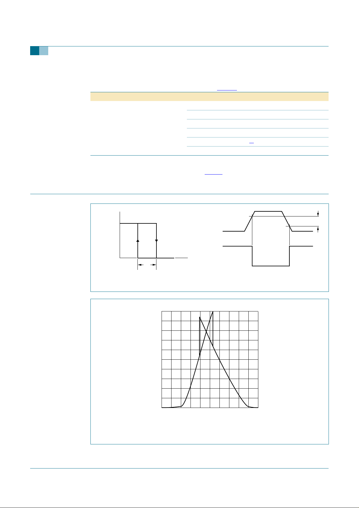
Fig 8. Definition of VT+, VT− and V
5
I
CC
(mA)
4
3
2
1
0
0 0.6 1.2 3
I
mna207
H
VCC = 3.0 V.
Fig 9. Typical transfer characteristic
V
O
VT− at 20 % and VT+ at 70 %
mna582
1.8 2.4
(V)
V
I
mna208
9397 750 14592 © Koninklijke Philips Electronics N.V. 2005. All rights reserved.
Product data sheet Rev. 03 — 15 February 2005 9 of 16
Page 10
Philips Semiconductors
15. Application information
74ALVC14
Hex inverting Schmitt trigger
2.5
I
CC
(mA)
2.0
1.5
1.0
0.5
2.1 2.7 3.9
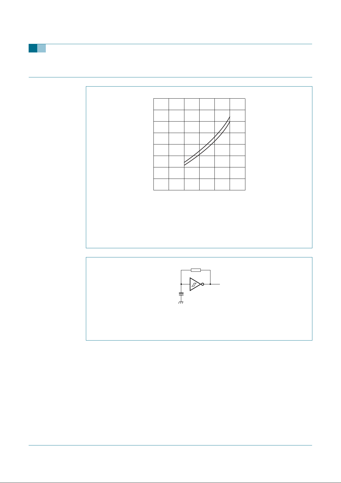
(1) Positive-going edge.
(2) Negative going-edge.
Linear change of VI between 0.8 V to 2.0 V.
All values given are typical unless otherwise specified.
(1)
(2)
3.32.4 3.0 3.6
mna581
(V)
V
CC
Fig 10. Average supply current as a function of supply voltage
1
1
f
≈=
---
--------------------- -
T
0.8 RC×
at VCC = 3.0 V.
Fig 11. Relaxation oscillator
R
C
mna035
9397 750 14592 © Koninklijke Philips Electronics N.V. 2005. All rights reserved.
Product data sheet Rev. 03 — 15 February 2005 10 of 16
Page 11
Philips Semiconductors
16. Package outline
74ALVC14
Hex inverting Schmitt trigger
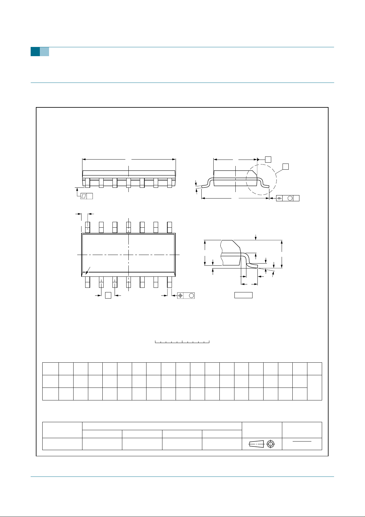
SO14: plastic small outline package; 14 leads; body width 3.9 mm
D
c
y
Z
14
pin 1 index
1
e
8
A
2
7
w M
b
p
SOT108-1
E
H
E
A
1
detail X
A
X
v M
A
Q
(A )
L
p
L
A
3
θ
0 2.5 5 mm
scale
DIMENSIONS (inch dimensions are derived from the original mm dimensions)
mm
OUTLINE
VERSION
SOT108-1
A
A1A2A3b
max.
0.25
1.75
0.10
0.010
0.069
0.004
p
1.45
1.25
0.057
0.049
IEC JEDEC JEITA
076E06 MS-012
0.25
0.01
0.49
0.36
0.019
0.014
0.25
0.19
0.0100
0.0075
UNIT
inches
Note
1. Plastic or metal protrusions of 0.15 mm (0.006 inch) maximum per side are not included.
(1)E(1)
cD
8.75
8.55
0.35
0.34
REFERENCES
eHELLpQZywv θ
4.0
3.8
0.16
0.15
1.27
0.05
6.2
5.8
0.244
0.228
0.041
1.05
1.0
0.4
0.039
0.016
0.7
0.25
0.6
0.028
0.01 0.004
0.024
EUROPEAN
PROJECTION
0.25 0.1
0.01
(1)
0.7
0.3
0.028
0.012
ISSUE DATE
99-12-27
03-02-19
o
8
o
0
Fig 12. Package outline SOT108-1 (SO14)
9397 750 14592 © Koninklijke Philips Electronics N.V. 2005. All rights reserved.
Product data sheet Rev. 03 — 15 February 2005 11 of 16
Page 12
Philips Semiconductors
74ALVC14
Hex inverting Schmitt trigger
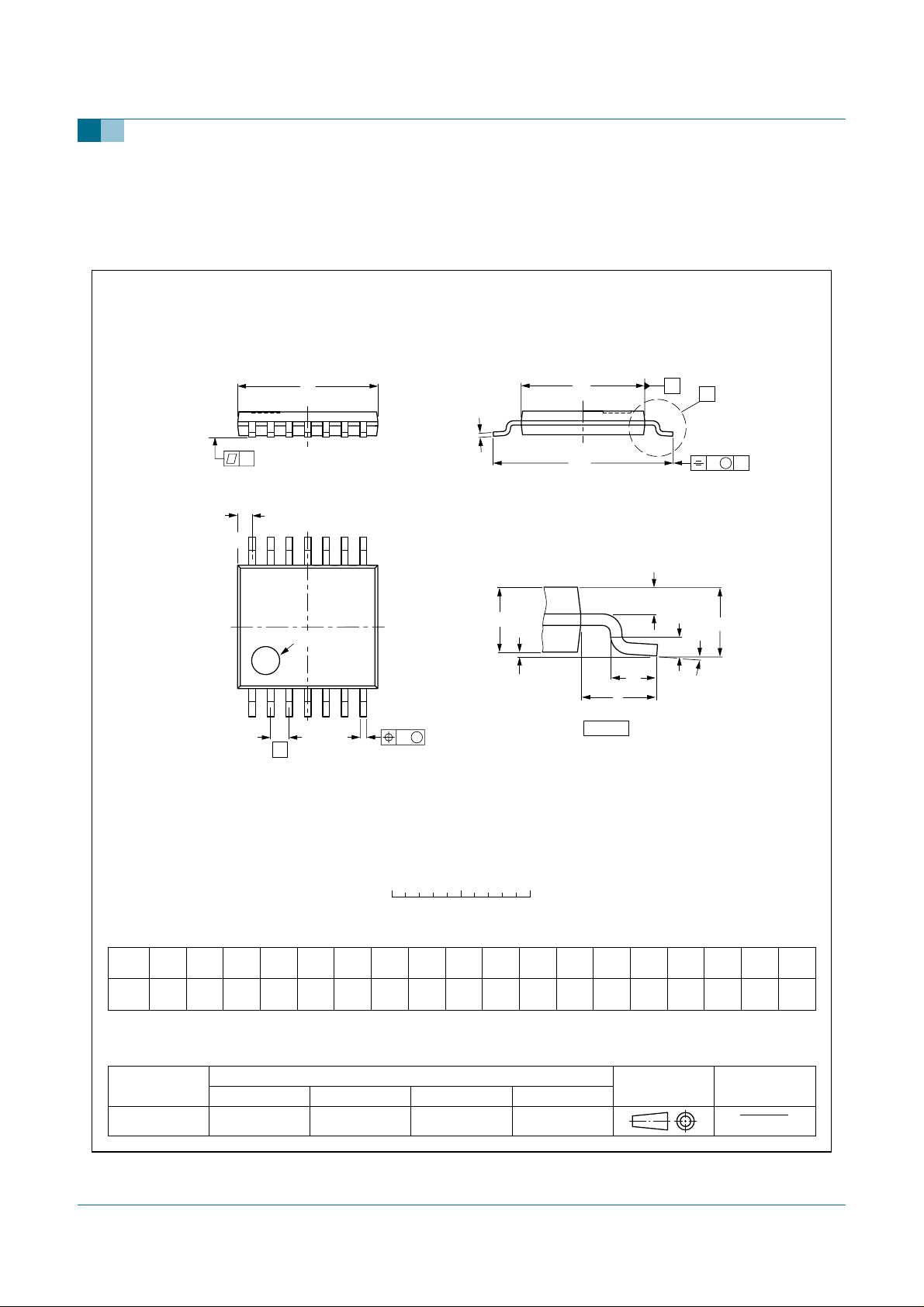
TSSOP14: plastic thin shrink small outline package; 14 leads; body width 4.4 mm
D
c
y
Z
14
pin 1 index
8
17
w M
b
e
p
A
2
A
1
E
H
E
L
detail X
SOT402-1
A
X
v M
A
Q
(A )
3
A
θ
L
p
0 2.5 5 mm
scale
DIMENSIONS (mm are the original dimensions)
UNIT A1A2A3b
Notes
1. Plastic or metal protrusions of 0.15 mm maximum per side are not included.
2. Plastic interlead protrusions of 0.25 mm maximum per side are not included.
A
max.
0.15
mm
1.1
OUTLINE
VERSION
SOT402-1 MO-153
0.05
0.95
0.25
0.80
IEC JEDEC JEITA
p
0.30
0.19
(1)E(2) (1)
cD
0.2
5.1
0.1
4.9
REFERENCES
eHELLpQZywv θ
4.5
4.3
0.65
6.6
6.2
0.75
0.50
0.4
0.3
EUROPEAN
PROJECTION
0.13 0.10.21
0.72
0.38
ISSUE DATE
99-12-27
03-02-18
o
8
o
0
Fig 13. Package outline SOT402-1 (TSSOP14)
9397 750 14592 © Koninklijke Philips Electronics N.V. 2005. All rights reserved.
Product data sheet Rev. 03 — 15 February 2005 12 of 16
Page 13
Philips Semiconductors
74ALVC14
Hex inverting Schmitt trigger
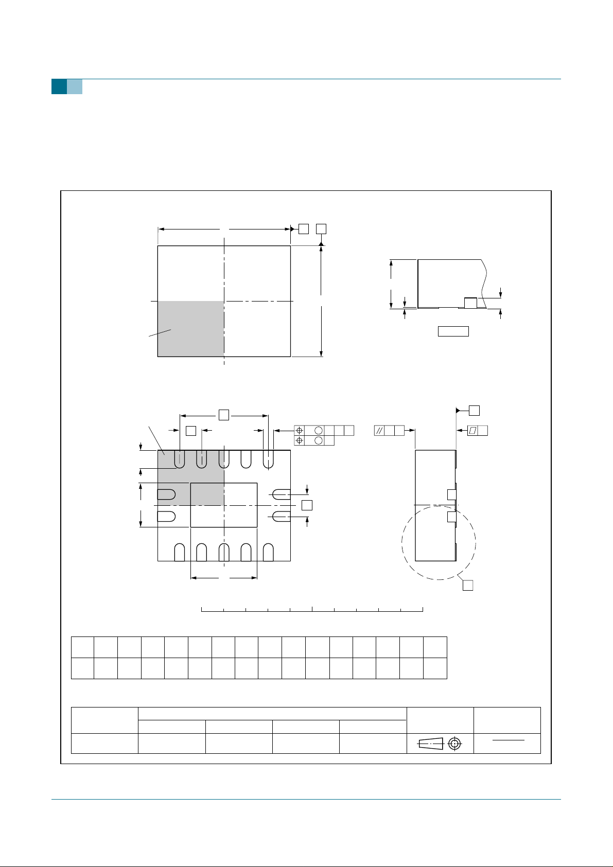
DHVQFN14: plastic dual in-line compatible thermal enhanced very thin quad flat package; no leads;
14 terminals; body 2.5 x 3 x 0.85 mm
A
D
B
A
A
E
1
SOT762-1
c
terminal 1
index area
terminal 1
index area
L
1
E
h
14
DIMENSIONS (mm are the original dimensions)
Note
1. Plastic or metal protrusions of 0.075 mm maximum per side are not included.
(1)
A
UNIT
mm
OUTLINE
VERSION
SOT762-1 MO-241 - - -- - -
max.
A
0.05
0.00
1
b
0.30
0.18
e
26
13
c
0.2
IEC JEDEC JEITA
e
1
b
9
D
h
0 2.5 5 mm
D
h
(1)
E
E
h
2.6
1.15
2.4
0.85
REFERENCES
D
3.1
2.9
(1)
1.65
1.35
v
w
7
e
8
scale
0.51
detail X
C
M
ACCB
M
e
L
1
0.5
2
0.3
y
w
0.1v0.05
C
1
ye
y
0.05 0.1
EUROPEAN
PROJECTION
1
y
X
ISSUE DATE
02-10-17
03-01-27
Fig 14. Package outline SOT762-1 (DHVQFN14)
9397 750 14592 © Koninklijke Philips Electronics N.V. 2005. All rights reserved.
Product data sheet Rev. 03 — 15 February 2005 13 of 16
Page 14

Philips Semiconductors
Hex inverting Schmitt trigger
74ALVC14
17. Revision history
Table 12: Revision history
Document ID Release date Data sheet status Change notice Doc. number Supersedes
74ALVC14_3 20050215 Product data sheet - 9397 750 14592 74ALVC14_2
Modifications:
74ALVC14_2 20030514 Product specification - 9397 750 11257 74ALVC14_1
74ALVC14_1 20030203 Product specification - 9397 750 10452 -
• The format of this data sheet is redesigned to comply with the current presentation and
information standard of Philips Semiconductors.
• General text updates.
9397 750 14592 © Koninklijke Philips Electronics N.V. 2005. All rights reserved.
Product data sheet Rev. 03 — 15 February 2005 14 of 16
Page 15

Philips Semiconductors
18. Data sheet status
74ALVC14
Hex inverting Schmitt trigger
Level Data sheet status
I Objective data Development This data sheet contains data from the objective specification for product development. Philips
II Preliminary data Qualification This datasheet contains data fromthe preliminary specification. Supplementarydatawill be published
III Product data Production This data sheet contains data from the product specification. Philips Semiconductors reserves the
[1] Please consult the most recently issued data sheet before initiating or completing a design.
[2] The product status of the device(s) described in this data sheet may have changed since this data sheet was published. The latest information is available on the Internet at
URL http://www.semiconductors.philips.com.
[3] For data sheets describing multiple type numbers, the highest-level product status determines the data sheet status.
[1]
Product status
19. Definitions
Short-form specification — The data in a short-form specification is
extracted from a full data sheet with the same type number and title. For
detailed information see the relevant data sheet or data handbook.
Limiting values definition — Limiting values given are in accordance with
the Absolute Maximum Rating System (IEC 60134). Stress above one or
more of the limiting values may cause permanent damage to the device.
These are stress ratings only and operation of the device at these or at any
other conditions above those given in the Characteristics sections of the
specification is not implied. Exposure to limiting values for extended periods
may affect device reliability.
Application information — Applications that are described herein for any
of these products are for illustrative purposes only. Philips Semiconductors
make no representation or warrantythat such applications will be suitable for
the specified use without further testing or modification.
[2] [3]
Definition
Semiconductors reserves the right to change the specification in any manner without notice.
at a laterdate. Philips Semiconductors reserves therightto change the specification without notice,in
order to improve the design and supply the best possible product.
right to make changesat any time in order to improve the design, manufacturing andsupply. Relevant
changes will be communicated via a Customer Product/Process Change Notification (CPCN).
20. Disclaimers
Life support — These products are not designed for use in life support
appliances, devices, or systems where malfunction of these products can
reasonably be expected to result in personal injury. Philips Semiconductors
customers using or selling these products for use in such applications do so
at their own risk and agree to fully indemnify Philips Semiconductors for any
damages resulting from such application.
Right to make changes — Philips Semiconductors reserves the right to
make changes in the products - including circuits, standard cells, and/or
software - described or contained herein in order to improve design and/or
performance. When the product is in full production (status ‘Production’),
relevant changes will be communicated via a Customer Product/Process
Change Notification (CPCN). Philips Semiconductors assumes no
responsibility or liability for the use of any of these products, conveys no
license or title under any patent, copyright, or mask work right to these
products, andmakes norepresentations or warrantiesthat these productsare
free frompatent, copyright, or maskwork right infringement, unlessotherwise
specified.
21. Contact information
For additional information, please visit: http://www.semiconductors.philips.com
For sales office addresses, send an email to: [email protected]
9397 750 14592 © Koninklijke Philips Electronics N.V. 2005. All rights reserved.
Product data sheet Rev. 03 — 15 February 2005 15 of 16
Page 16

Philips Semiconductors
22. Contents
1 General description. . . . . . . . . . . . . . . . . . . . . . 1
2 Features . . . . . . . . . . . . . . . . . . . . . . . . . . . . . . . 1
3 Quick reference data . . . . . . . . . . . . . . . . . . . . . 1
4 Ordering information. . . . . . . . . . . . . . . . . . . . . 2
5 Functional diagram . . . . . . . . . . . . . . . . . . . . . . 3
6 Pinning information. . . . . . . . . . . . . . . . . . . . . . 4
6.1 Pinning . . . . . . . . . . . . . . . . . . . . . . . . . . . . . . . 4
6.2 Pin description . . . . . . . . . . . . . . . . . . . . . . . . . 4
7 Functional description . . . . . . . . . . . . . . . . . . . 5
7.1 Function table . . . . . . . . . . . . . . . . . . . . . . . . . . 5
8 Limiting values. . . . . . . . . . . . . . . . . . . . . . . . . . 5
9 Recommended operating conditions. . . . . . . . 6
10 Static characteristics. . . . . . . . . . . . . . . . . . . . . 6
11 Dynamic characteristics . . . . . . . . . . . . . . . . . . 7
12 Waveforms . . . . . . . . . . . . . . . . . . . . . . . . . . . . . 7
13 Transfer characteristics. . . . . . . . . . . . . . . . . . . 8
14 Waveforms transfer characteristics. . . . . . . . . 9
15 Application information. . . . . . . . . . . . . . . . . . 10
16 Package outline . . . . . . . . . . . . . . . . . . . . . . . . 11
17 Revision history. . . . . . . . . . . . . . . . . . . . . . . . 14
18 Data sheet status. . . . . . . . . . . . . . . . . . . . . . . 15
19 Definitions . . . . . . . . . . . . . . . . . . . . . . . . . . . . 15
20 Disclaimers. . . . . . . . . . . . . . . . . . . . . . . . . . . . 15
21 Contact information . . . . . . . . . . . . . . . . . . . . 15
74ALVC14
Hex inverting Schmitt trigger
© Koninklijke Philips Electronics N.V. 2005
All rights are reserved. Reproduction in whole or in part is prohibited without the prior
written consent of the copyright owner. The information presented in this document does
not form partof any quotation or contract, is believed to be accurate and reliable and may
be changed without notice. No liability will be accepted by the publisher for any
consequence of its use. Publication thereof does not convey nor imply any license under
patent- or other industrial or intellectual property rights.
Published in The Netherlands
Date of release: 15 February 2005
Document number: 9397 750 14592
 Loading...