

Page 1

INTEGRATED CIRCUITS
DATA SH EET
74AHC138; 74AHCT138
3-to-8 line decoder/demultiplexer;
inverting
Product specification
Supersedes data of 1999 Mar 31
File under Integrated Circuits, IC06
1999 Sep 27
Page 2

Philips Semiconductors Product specification
3-to-8 line decoder/demultiplexer; inverting
FEATURES
• ESD protection:
HBM EIA/JESD22-A114-A
exceeds 2000 V
MM EIA/JESD22-A115-A
exceeds 200 V
CDM EIA/JESD22-C101
exceeds 1000 V
• Balanced propagation delays
• All inputs have Schmitt-trigger
actions
• Multiple input enable for easy
expansion
• Ideal for memory chip select
decoding
• Inputs accept voltages higher than
V
CC
• For AHC only:
operates with CMOS input levels
• For AHCT only:
operates with TTL input levels
• Specified from
−40 to +85 and +125 °C.
DESCRIPTION
The 74AHC/AHCT138 are high-speed Si-gate CMOS devices and are pin
compatible with low power Schottky TTL (LSTTL). They are specified in
compliance with JEDEC standard No. 7A.
The 74AHC/AHCT138 decoders accept three binary weighted address inputs
(A0,A1and A2) and when enabled, provide 8 mutually exclusive active LOW
outputs (Y0to Y7).
The ‘138’ features three enable inputs: two active LOW (E1and E2) and one
active HIGH(E3). Every output will be HIGH unless E1and E2are LOW and E
is HIGH.
This multiple enable function allows easy parallel expansion of the ‘138’ to a
1-of-32 (5 to 32 lines) decoder with just four ‘138’ ICs and one inverter.
The ‘138’ can be used as an eight output demultiplexer by using one of the
active LOW enable inputs as the data input and the remaining enable inputs as
strobes. Unused enable inputs must be permanently tied to their appropriate
active HIGH or LOW state.
The ‘138’ is identical to the ‘238’ but has inverting outputs.
74AHC138;
74AHCT138
3
QUICK REFERENCE DATA
GND = 0 V; T
=25°C; tr=tf≤3.0 ns.
amb
SYMBOL PARAMETER CONDITIONS
t
PHL/tPLH
C
I
C
O
C
PD
propagation delay Anto Y
propagation delay E
n
to Yn; Ento YnCL= 15 pF; VCC= 5 V 4.2 4.3 ns
3
input capacitance VI=VCCor GND 3.0 3.0 pF
output capacitance 4.0 4.0 pF
power dissipation capacitance CL= 50 pF; f = 1 MHz;
CL= 15 pF; VCC= 5 V 4.4 4.4 ns
notes 1 and 2
Notes
1. C
is used to determine the dynamic power dissipation (PDin µW).
PD
P
D=CPD
× V
2
× fi+ ∑ (CL× V
CC
2
× fo) where:
CC
fi= input frequency in MHz;
fo= output frequency in MHz;
∑ (CL× V
2
× fo) = sum of outputs;
CC
CL= output load capacitance in pF;
VCC= supply voltage in Volts.
2. The condition is VI= GND to VCC.
TYPICAL
UNIT
AHC AHCT
18 23 pF
1999 Sep 27 2
Page 3

Philips Semiconductors Product specification
3-to-8 line decoder/demultiplexer; inverting
74AHC138;
74AHCT138
FUNCTION TABLE
See note 1.
INPUT OUTPUT
E
HXXXXXHHHHHHHH
XHXXXXHHHHHHHH
XXLXXXHHHHHHHH
LLHLLLLHHHHHHH
LLHHL LHLHHHHHH
LLHLHLHHLHHHHH
LLHHHLHHHLHHHH
LLHL LHHHHHLHHH
LLHHLHHHHHHLHH
LLHLHHHHHHHHLH
LLHHHHHHHHHHHL
Note
1. H = HIGH voltage level;
L = LOW voltage level;
X = don’t care.
E
1
E
2
A
3
A
0
A
1
Y
2
Y
0
Y
1
Y
2
Y
3
Y
4
Y
5
Y
6
7
ORDERING INFORMATION
OUTSIDE NORTH
AMERICA
NORTH AMERICA
PINS PACKAGE MATERIAL CODE
PACKAGES
74AHC138D 74AHC138D 16 SO plastic SOT109-1
74AHC138PW 74AHC138PW DH 16 TSSOP plastic SOT403-1
74AHCT138D 74AHCT138D 16 SO plastic SOT109-1
74AHCT138PW 74AHCT138PW DH 16 TSSOP plastic SOT403-1
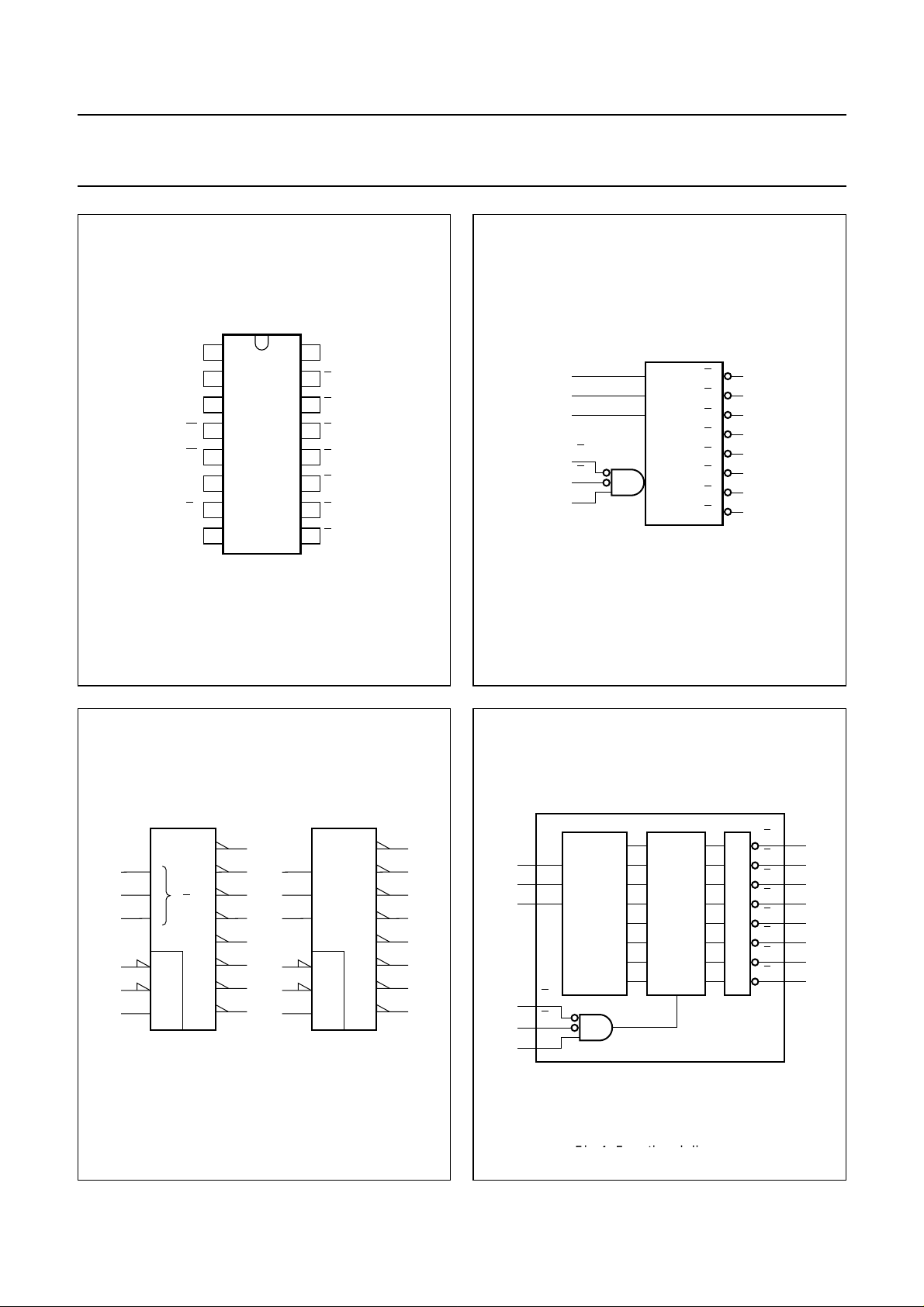
PINNING
PIN SYMBOL DESCRIPTION
1, 2 and 3 A
4 and 5
6E
7, 9, 10 11, 12, 13, 14 and 15
and A2address inputs
0,A1
E1and E
3
Y7to Y
2
0
enable inputs (active LOW)
enable input (active HIGH)
outputs (active LOW)
8 GND ground (0 V)
16 V
CC
DC supply voltage
1999 Sep 27 3
Page 4
Philips Semiconductors Product specification
3-to-8 line decoder/demultiplexer; inverting
handbook, halfpage
A
A
A
E
E
E
Y
GND
1
0
2
1
3
2
4
1
2
3
7
138
5
6
7
8
MNA369
V
16
CC
Y
15
0
Y
14
1
Y
13
2
Y
12
3
Y
11
4
Y
10
5
Y
9
6
handbook, halfpage
74AHC138;
74AHCT138
Y
1
2
3
E
1
4
E
2
5
E
3
6
0
A
1
A
2
MNA370
15A
0
Y
14
1
13
Y
2
12
Y
3
11
Y
4
10
Y
5
9
Y
6
7
Y
7
handbook, halfpage
1
2
3
4
5
6
Fig.1 Pin configuration.
DX
0
0
G
7
2
&
(a) (b)
15
0
14
1
13
2
12
3
11
4
10
5
9
6
7
7
1
2
3
4
5
6
Fig.2 Logic symbol.
handbook, halfpage
X/Y
1
2
4
&
MNA371
EN
15
0
14
1
13
2
12
3
11
4
10
5
9
6
7
7
A
0
1
A
2
1
A
3
2
3-to-8
DECODER
E
4
1
E
5
2
E
6
3
ENABLE
EXITING
Y
0
Y
1
Y
2
Y
3
Y
4
Y
5
Y
6
Y
7
MNA372
15
14
13
12
11
10
9
7
Fig.3 IEC logic symbol.
1999 Sep 27 4
Fig.4 Functional diagram.
Fig.4 Functional diagram.
Page 5

Philips Semiconductors Product specification
3-to-8 line decoder/demultiplexer; inverting
74AHC138;
74AHCT138
RECOMMENDED OPERATING CONDITIONS
SYMBOL PARAMETER CONDITIONS
V
CC
V
I
V
O
T
amb
DC supply voltage 2.0 5.0 5.5 4.5 5.0 5.5 V
input voltage 0 − 5.5 0 − 5.5 V
output voltage 0 − V
operating ambient temperature
range
see DC and AC
characteristics per
device
t
(∆t/∆f) input rise and fall rates VCC= 3.3 V ±0.3 V −−100 −−−ns/V
r,tf
=5V±0.5 V −−20 −−20
V
CC
LIMITING VALUES
In accordance with the Absolute Maximum Rating System (IEC 134); voltages are referenced to GND (ground= 0 V).
SYMBOL PARAMETER CONDITIONS MIN. MAX. UNIT
V
CC
V
I
I
IK
I
OK
I
O
I
CC
T
stg
P
D
DC supply voltage −0.5 +7.0 V
input voltage range −0.5 +7.0 V
DC input diode current VI< −0.5 V; note 1 −−20 mA
DC output diode current VO< −0.5 Vor VO>VCC+ 0.5 V; note 1 −±20 mA
DC output source or sink current −0.5V<VO<VCC+ 0.5 V −±25 mA
DC VCC or GND current −±75 mA
storage temperature range −65 +150 °C
power dissipation per package for temperature range: −40 to +125 °C; note 2 − 500 mW
74AHC 74AHCT
UNIT
MIN. TYP. MAX. MIN. TYP. MAX.
0 − V
CC
CC
V
−40 +25 +85 −40 +25 +85 °C
−40 +25 +125 −40 +25 +125 °C
Notes
1. The input and output voltage ratings may be exceeded if the input and output current ratings are observed.
2. For SO packages: above 70 °C the value of P
derates linearly with 8 mW/K.
D
For TSSOP packages: above 60 °C the value of PDderates linearly with 5.5 mW/K.
1999 Sep 27 5
Page 6

Philips Semiconductors Product specification
3-to-8 line decoder/demultiplexer; inverting
DC CHARACTERISTICS
74AHC family
Over recommended operating conditions; voltages are referenced to GND (ground=0V).
amb
(°C)
SYMBOL PARAMETER
V
IH
HIGH-level input
voltage
V
IL
LOW-level input
voltage
V
OH
HIGH-level output
voltage; all
outputs
HIGH-level output
voltage
V
OL
LOW-level output
voltage; all
outputs
LOW-level output
voltage
I
I
input leakage
current
I
OZ
3-state output
OFF current
I
CC
quiescent supply
current
C
I
input capacitance −−310−10 − 10 pF
TEST CONDITIONS T
25 −40 to +85 −40 to +125
OTHER VCC(V)
MIN. TYP. MAX. MIN. MAX. MIN. MAX.
2.0 1.5 −−1.5 − 1.5 − V
3.0 2.1 −−2.1 − 2.1 −
5.5 3.85 −−3.85 − 3.85 −
2.0 −− 0.5 − 0.5 − 0.5 V
3.0 −− 0.9 − 0.9 − 0.9
5.5 −− 1.65 − 1.65 − 1.65
VI=VIHor VIL;
IO= −50 µA
2.0 1.9 2.0 − 1.9 − 1.9 − V
3.0 2.9 3.0 − 2.9 − 2.9 −
4.5 4.4 4.5 − 4.4 − 4.4 −
V
I=VIH
or VIL;
3.0 2.58 −−2.48 − 2.40 − V
IO= −4.0 mA
V
I=VIH
or VIL;
4.5 3.94 −−3.8 − 3.70 −
IO= −8.0 mA
VI=VIHor VIL;
IO=50µA
2.0 − 0 0.1 − 0.1 − 0.1 V
3.0 − 0 0.1 − 0.1 − 0.1
4.5 − 0 0.1 − 0.1 − 0.1
V
I=VIH
or VIL;
3.0 −− 0.36 − 0.44 − 0.55 V
IO=4mA
V
I=VIH
or VIL;
4.5 −− 0.36 − 0.44 − 0.55
IO=8mA
VI=VCCor GND 5.5 −− 0.1 − 1.0 − 2.0 µA
VI=VIHor VIL;
5.5 −− ±0.25 −±2.5 −±10.0 µA
VO=VCCor GND
VI=VCCor GND;
5.5 −− 4.0 − 40 − 80 µA
IO=0
74AHC138;
74AHCT138
UNIT
1999 Sep 27 6
Page 7

Philips Semiconductors Product specification
3-to-8 line decoder/demultiplexer; inverting
74AHCT family
Over recommended operating conditions; voltages are referenced to GND (ground=0V).
SYMBOL PARAMETER
V
IH
HIGH-level input
voltage
V
IL
LOW-level input
voltage
V
OH
HIGH-level output
voltage; all
outputs
HIGH-level output
voltage
V
OL
LOW-level output
voltage; all
outputs
LOW-level output
voltage
I
I
input leakage
current
I
OZ
3-state output
OFF current
I
CC
quiescent supply
current
∆I
CC
additional
quiescent supply
current per input
pin
C
I
input capacitance −−310−10 − 10 pF
TEST CONDITIONS T
25 −40 to +85 −40 to +125
OTHER VCC(V)
MIN. TYP. MAX. MIN. MAX. MIN. MAX.
4.5 to 5.5 2.0 −−2.0 − 2.0 − V
4.5 to 5.5 −− 0.8 − 0.8 − 0.8 V
VI=VIHor VIL;
4.5 4.4 4.5 − 4.4 − 4.4 − V
IO= −50 µA
V
I=VIH
or VIL;
4.5 3.94 −−3.8 − 3.70 − V
IO= −8.0 mA
VI=VIHor VIL;
4.5 − 0 0.1 − 0.1 − 0.1 V
IO=50µA
V
I=VIH
or VIL;
4.5 −− 0.36 − 0.44 − 0.55 V
IO=8mA
VI=VIHor V
VI=VIHor VIL;
5.5 −− 0.1 − 1.0 − 2.0 µA
IL
5.5 −− ±0.25 −±2.5 −±10.0 µA
VO=VCCor GND
per input pin;
other inputs at
VCCor GND;
IO=0
VI=VCCor GND;
5.5 −− 4.0 − 40 − 80 µA
IO=0
VI=VCC− 2.1 V
4.5 to 5.5 −− 1.35 − 1.5 − 1.5 mA
other inputs at
VCCor GND;
IO=0
amb
(°C)
74AHC138;
74AHCT138
UNIT
1999 Sep 27 7
Page 8
Philips Semiconductors Product specification
3-to-8 line decoder/demultiplexer; inverting
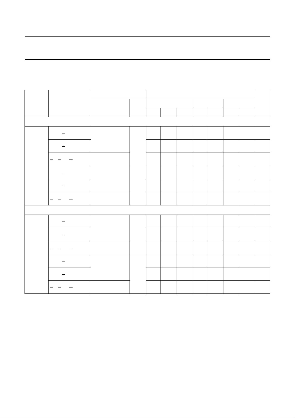
AC CHARACTERISTICS
Type 74AHC138
GND = 0 V; tr=tf≤3.0 ns.
TEST CONDITIONS T
SYMBOL PARAMETER
VCC= 3.0 to 3.6 V; note 1
t
PHL/tPLH
propagation delay
Anto Y
n
propagation delay
E
to Y
3
n
propagation delay
E1, E2to Y
n
propagation delay
A
to Y
n
n
propagation delay
E
to Y
3
n
propagation delay
E1, E2to Y
n
VCC= 4.5 to 5.5 V; note 2
WAVEFORMS C
L
see Figs 5 and 7 15 pF − 6.0 11.4 1.0 13.0 1.0 14.5 ns
see Figs 6 and 7 − 5.7 11.4 1.0 13.5 1.0 14.5 ns
see Figs 5 and 7 50 pF − 8.6 15.8 1.0 18.0 1.0 20.0 ns
see Figs 6 and 7 − 8.2 14.9 1.0 17.0 1.0 19.0 ns
74AHC138;
74AHCT138
(°C)
amb
25 −40 to +85 −40 to +125
MIN. TYP. MAX. MIN. MAX. MIN. MAX.
− 5.8 12.8 1.0 15.0 1.0 16.0 ns
− 8.2 16.3 1.0 18.5 1.0 20.5 ns
UNIT
t
PHL/tPLH
propagation delay
Anto Y
n
propagation delay
E
to Y
3
n
propagation delay
E1, E2to Y
n
propagation delay
A
to Y
n
n
propagation delay
E
to Y
3
n
propagation delay
E1, E2to Y
n
Notes
1. Typical values at V
CC
= 3.3 V.
2. Typical values at VCC= 5.0 V.
see Figs 5 and 7 15 pF − 4.4 8.1 1.0 9.5 1.0 10.5 ns
− 4.2 8.1 1.0 9.5 1.0 10.5 ns
see Figs 6 and 7 − 4.2 8.1 1.0 9.5 1.0 10.5 ns
see Figs 5 and 7 50 pF − 6.3 10.1 1.0 11.5 1.0 13.0 ns
− 6.0 10.1 1.0 11.5 1.0 13.0 ns
see Figs 6 and 7 − 6.0 10.1 1.0 11.5 1.0 13.0 ns
1999 Sep 27 8
Page 9

Philips Semiconductors Product specification
3-to-8 line decoder/demultiplexer; inverting
Type 74AHCT138
GND = 0 V; tr=tf≤3.0 ns.
TEST CONDITIONS T
SYMBOL PARAMETER
VCC= 4.5 to 5.5 V; note 1
t
PHL/tPLH
propagation delay
Anto Y
n
propagation delay
to Y
E
3
n
propagation delay
E1, E2to Y
n
propagation delay
A
to Y
n
n
propagation delay
to Y
E
3
n
propagation delay
E1, E2to Y
n
WAVEFORMS C
L
see Figs 5 and 7 15 pF − 4.4 10.4 1.0 12.0 1.0 13.0 ns
see Figs 6 and 7 − 4.3 9.6 1.0 11.0 1.0 12.0 ns
see Figs 5 and 7 50 pF − 6.2 11.4 1.0 13.0 1.0 14.5 ns
see Figs 6 and 7 − 6.2 10.6 1.0 12.0 1.0 13.5 ns
74AHC138;
74AHCT138
(°C)
amb
25 −40 to +85 −40 to +125
MIN. TYP. MAX. MIN. MAX. MIN. MAX.
− 4.3 9.1 1.0 10.5 1.0 11.5 ns
− 6.2 10.1 1.0 11.5 1.0 13.0 ns
UNIT
Note
1. Typical values at V
CC
= 5.0 V.
1999 Sep 27 9
Page 10
Philips Semiconductors Product specification
3-to-8 line decoder/demultiplexer; inverting
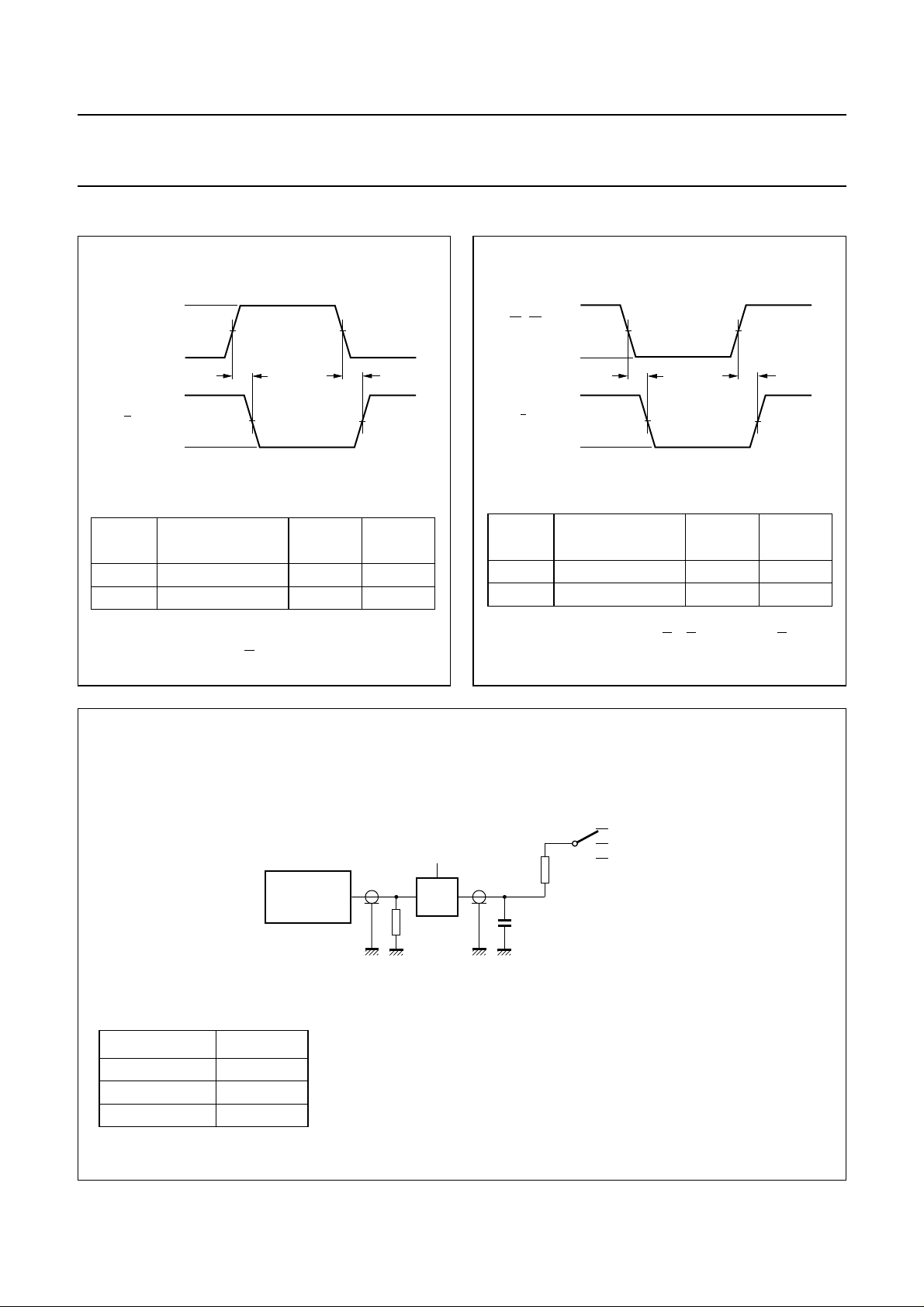
AC WAVEFORMS
An, E
INPUT
Y
n
V
CC
3
GND
t
PHL
V
OH
V
OL
VI INPUT
REQUIREMENTS
CC
(1)
V
M
t
PLH
(1)
V
M
MNA373
V
M
INPUT
50% V
(1)
CC
(1)
V
M
OUTPUT
50% V
CC
CC
handbook, halfpage
FAMILY
AHC GND to V
AHCT GND to 3.0 V 1.5 V 50% V
74AHC138;
74AHCT138
E1, E
INPUT
Y
n
V
CC
2
GND
t
PHL
V
OH
V
OL
VI INPUT
REQUIREMENTS
CC
(1)
V
M
(1)
V
M
(1)
V
M
INPUT
50% VCC50% V
handbook, halfpage
FAMILY
AHC GND to V
AHCT GND to 3.0 V 1.5 V 50% V
t
PLH
MNA374
(1)
V
M
OUTPUT
CC
CC
Fig.5 The address input (An) and enable input
(E3) to output (Yn) propagation delays.
handbook, full pagewidth
PULSE
GENERATOR
TEST S
t
PLH/tPHL
t
PLZ/tPZL
t
PHZ/tPZH
open
V
CC
GND
1
Fig.6 The enable input (E1, E2) to output (Yn)
propagation delays.
S1
V
CC
V
CC
V
I
R
D.U.T.
T
V
O
1000 Ω
C
L
MNA219
open
GND
Fig.7 Load circuitry for switching times.
1999 Sep 27 10
Page 11
Philips Semiconductors Product specification
3-to-8 line decoder/demultiplexer; inverting
PACKAGE OUTLINES
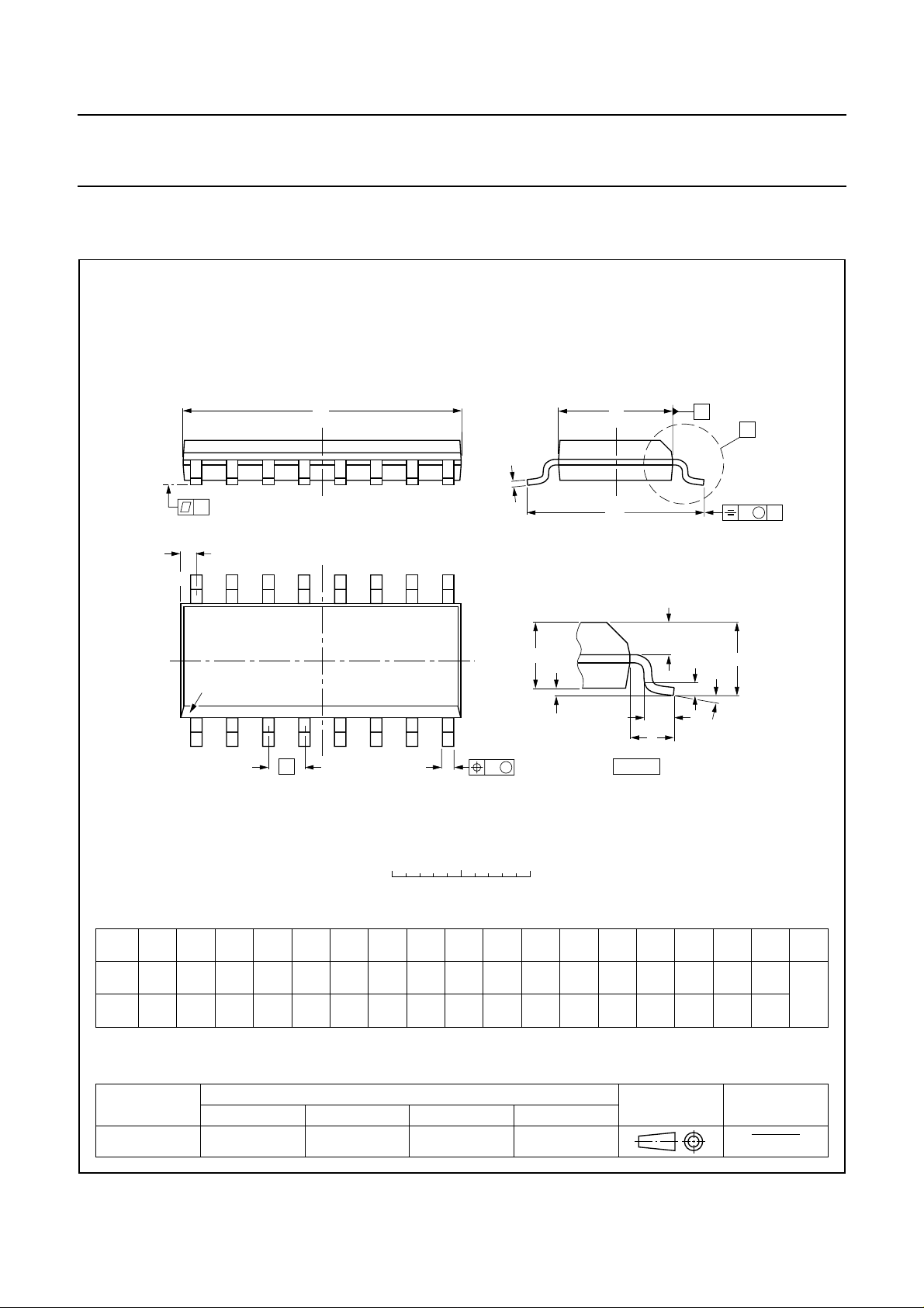
SO16: plastic small outline package; 16 leads; body width 3.9 mm
D
c
y
Z
16
9
74AHC138;
74AHCT138
SOT109-1
E
H
E
A
X
v M
A
pin 1 index
1
e
0 2.5 5 mm
DIMENSIONS (inch dimensions are derived from the original mm dimensions)
UNIT
mm
inches
Note
1. Plastic or metal protrusions of 0.15 mm maximum per side are not included.
A
max.
1.75
0.069
A1A2A
0.25
1.45
0.10
1.25
0.010
0.057
0.004
0.049
0.25
0.01
b
3
p
0.49
0.25
0.36
0.19
0.0100
0.019
0.0075
0.014
(1)E(1) (1)
cD
10.0
9.8
0.39
0.38
8
b
p
scale
eHELLpQZywv θ
4.0
1.27
3.8
0.16
0.050
0.15
w M
6.2
5.8
0.244
0.228
A
2
1.05
0.041
Q
A
1
detail X
1.0
0.7
0.4
0.6
0.028
0.039
0.020
0.016
(A )
L
p
L
0.25 0.1
0.25
0.01
0.01 0.004
A
3
θ
0.7
0.3
0.028
0.012
o
8
o
0
OUTLINE
VERSION
SOT109-1
IEC JEDEC EIAJ
076E07S MS-012AC
REFERENCES
1999 Sep 27 11
EUROPEAN
PROJECTION
ISSUE DATE
95-01-23
97-05-22
Page 12
Philips Semiconductors Product specification
3-to-8 line decoder/demultiplexer; inverting
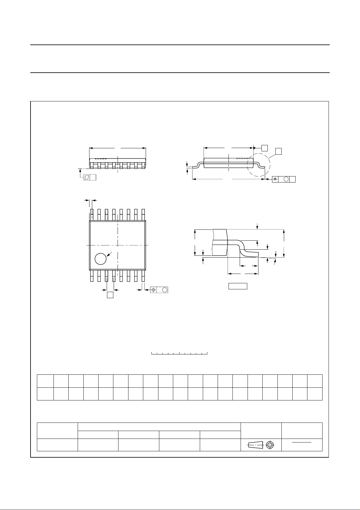
TSSOP16: plastic thin shrink small outline package; 16 leads; body width 4.4 mm
E
H
E
16
D
c
y
Z
9
74AHC138;
74AHCT138
A
X
v M
A
SOT403-1
pin 1 index
18
w M
b
e
DIMENSIONS (mm are the original dimensions)
UNIT A1A
Notes
1. Plastic or metal protrusions of 0.15 mm maximum per side are not included.
2. Plastic interlead protrusions of 0.25 mm maximum per side are not included.
A
max.
1.10
0.15
0.05
mm
OUTLINE
VERSION
SOT403-1 MO-153
A
0.25
b
3
p
0.30
0.19
2
0.95
0.80
IEC JEDEC EIAJ
p
0 2.5 5 mm
scale
(1)E(2) (1)
cD
0.2
5.1
0.1
4.9
REFERENCES
eHELLpQZywv θ
4.5
0.65
4.3
A
6.6
6.2
Q
(A )
2
A
1
L
p
L
detail X
0.75
0.4
0.50
0.3
EUROPEAN
PROJECTION
3
A
θ
0.13 0.10.21.0
0.40
0.06
ISSUE DATE
94-07-12
95-04-04
o
8
o
0
1999 Sep 27 12
Page 13

Philips Semiconductors Product specification
3-to-8 line decoder/demultiplexer; inverting
SOLDERING
Introduction to soldering surface mount packages
Thistextgives a very brief insighttoa complex technology.
A more in-depth account of soldering ICs can be found in
our
“Data Handbook IC26; Integrated Circuit Packages”
(document order number 9398 652 90011).
There is no soldering method that is ideal for all surface
mount IC packages. Wave soldering isnot always suitable
for surface mount ICs, or for printed-circuit boards with
high population densities. In these situations reflow
soldering is often used.
Reflow soldering
Reflow soldering requires solder paste (a suspension of
fine solder particles, flux and binding agent) to be applied
tothe printed-circuit board byscreen printing, stencilling or
pressure-syringe dispensing before package placement.
Several methods exist for reflowing; for example,
infrared/convection heating in a conveyor type oven.
Throughput times (preheating,soldering and cooling) vary
between 100 and 200 seconds depending on heating
method.
Typical reflow peak temperatures range from
215 to 250 °C. The top-surface temperature of the
packages should preferable be kept below 230 °C.
74AHC138;
74AHCT138
• Use a double-wave soldering method comprising a
turbulent wave with high upward pressure followed by a
smooth laminar wave.
• For packages with leads on two sides and a pitch (e):
– larger than or equal to 1.27 mm, the footprint
longitudinal axis is preferred to be parallel to the
transport direction of the printed-circuit board;
– smaller than 1.27 mm, the footprint longitudinal axis
must be parallel to the transport direction of the
printed-circuit board.
The footprint must incorporate solder thieves at the
downstream end.
• Forpackageswith leads on four sides, thefootprintmust
be placed at a 45° angle to the transport direction of the
printed-circuit board. The footprint must incorporate
solder thieves downstream and at the side corners.
During placement andbefore soldering, the package must
be fixed with a droplet of adhesive. The adhesive can be
applied by screen printing, pin transfer or syringe
dispensing. The package can be soldered after the
adhesive is cured.
Typical dwell time is 4 seconds at 250 °C.
A mildly-activated flux will eliminate the need for removal
of corrosive residues in most applications.
Manual soldering
Wave soldering
Conventional single wave soldering is not recommended
forsurfacemount devices (SMDs) or printed-circuitboards
with a high component density, as solder bridging and
non-wetting can present major problems.
To overcome these problems the double-wave soldering
method was specifically developed.
If wave soldering is used the following conditions must be
observed for optimal results:
Fix the component by first soldering two
diagonally-opposite end leads. Use a low voltage (24 V or
less) soldering iron applied to the flat part of the lead.
Contact time must be limited to 10 seconds at up to
300 °C.
When using a dedicated tool, all other leads can be
soldered in one operation within 2 to 5 seconds between
270 and 320 °C.
1999 Sep 27 13
Page 14

Philips Semiconductors Product specification
3-to-8 line decoder/demultiplexer; inverting
74AHC138;
74AHCT138
Suitability of surface mount IC packages for wave and reflow soldering methods
PACKAGE
BGA, SQFP not suitable suitable
HLQFP, HSQFP, HSOP, HTQFP, HTSSOP, SMS not suitable
(3)
PLCC
LQFP, QFP, TQFP not recommended
SSOP, TSSOP, VSO not recommended
Notes
1. All surface mount (SMD) packages are moisture sensitive. Depending upon the moisture content, the maximum
2. These packages are not suitable for wave soldering as a solder joint between the printed-circuit board and heatsink
3. If wave soldering is considered, then the package must be placed at a 45° angle to the solder wave direction.
4. Wave soldering is only suitable for LQFP, TQFP and QFP packages with a pitch (e) equal to or larger than 0.8 mm;
5. Wave soldering is only suitable for SSOP and TSSOP packages with a pitch (e) equal to or larger than 0.65 mm;it is
, SO, SOJ suitable suitable
temperature (with respect to time) and body size of the package, there is a risk that internal or external package
cracks may occur due to vaporization of the moisture in them (the so called popcorn effect). For details, refer to the
Drypack information in the
(at bottom version) can not be achieved, and as solder may stick to the heatsink (on top version).
The package footprint must incorporate solder thieves downstream and at the side corners.
it is definitely not suitable for packages with a pitch (e) equal to or smaller than 0.65 mm.
definitely not suitable for packages with a pitch (e) equal to or smaller than 0.5 mm.
“Data Handbook IC26; Integrated Circuit Packages; Section: Packing Methods”
WAVE REFLOW
(2)
SOLDERING METHOD
suitable
(3)(4)
(5)
suitable
suitable
(1)
.
DEFINITIONS
Data sheet status
Objective specification This data sheet contains target or goal specifications for product development.
Preliminary specification This data sheet contains preliminary data; supplementary data may be published later.
Product specification This data sheet contains final product specifications.
Limiting values
Limiting values given are in accordance with the Absolute Maximum Rating System (IEC 134). Stress above one or
more of the limiting values may cause permanent damage to the device. These are stress ratings only and operation
of the device at these or at any other conditions above those given in the Characteristics sections of the specification
is not implied. Exposure to limiting values for extended periods may affect device reliability.
Application information
Where application information is given, it is advisory and does not form part of the specification.
LIFE SUPPORT APPLICATIONS
These products are not designed for use in life support appliances, devices, or systems where malfunction of these
products can reasonably be expected to result in personal injury. Philips customers using or selling these products for
use in such applications do so at their own risk and agree to fully indemnify Philips for any damages resulting from such
improper use or sale.
1999 Sep 27 14
Page 15

Philips Semiconductors Product specification
3-to-8 line decoder/demultiplexer; inverting
NOTES
74AHC138;
74AHCT138
1999 Sep 27 15
Page 16

Philips Semiconductors – a w orldwide compan y
Argentina: see South America
Australia: 3 Figtree Drive, HOMEBUSH, NSW 2140,
Tel. +61 2 9704 8141, Fax. +61 2 9704 8139
Austria: Computerstr. 6, A-1101 WIEN, P.O. Box 213,
Tel. +43 1 60 101 1248, Fax. +43 1 60 101 1210
Belarus: Hotel Minsk Business Center, Bld. 3, r. 1211, Volodarski Str. 6,
220050 MINSK, Tel. +375 172 20 0733, Fax. +375 172 20 0773
Belgium: see The Netherlands
Brazil: see South America
Bulgaria: Philips Bulgaria Ltd., Energoproject, 15th floor,
51 James Bourchier Blvd., 1407 SOFIA,
Tel. +359 2 68 9211, Fax. +359 2 68 9102
Canada: PHILIPS SEMICONDUCTORS/COMPONENTS,
Tel. +1 800 234 7381, Fax. +1 800 943 0087
China/Hong Kong: 501 Hong Kong Industrial Technology Centre,
72 Tat Chee Avenue, Kowloon Tong, HONG KONG,
Tel. +852 2319 7888, Fax. +852 2319 7700
Colombia: see South America
Czech Republic: see Austria
Denmark: Sydhavnsgade 23, 1780 COPENHAGEN V,
Tel. +45 33 29 3333, Fax. +45 33 29 3905
Finland: Sinikalliontie 3, FIN-02630 ESPOO,
Tel. +358 9 615 800, Fax. +358 9 6158 0920
France: 51 Rue Carnot, BP317, 92156 SURESNES Cedex,
Tel. +33 1 4099 6161, Fax. +33 1 4099 6427
Germany: Hammerbrookstraße 69, D-20097 HAMBURG,
Tel. +49 40 2353 60, Fax. +49 40 2353 6300
Hungary: see Austria
India: Philips INDIA Ltd, Band Box Building, 2nd floor,
254-D, Dr. Annie Besant Road, Worli, MUMBAI 400 025,
Tel. +91 22 493 8541, Fax. +91 22 493 0966
Indonesia: PTPhilips Development Corporation,Semiconductors Division,
Gedung Philips, Jl. Buncit Raya Kav.99-100, JAKARTA 12510,
Tel. +62 21 794 0040 ext. 2501, Fax. +62 21 794 0080
Ireland: Newstead, Clonskeagh, DUBLIN 14,
Tel. +353 1 7640 000, Fax. +353 1 7640 200
Israel: RAPAC Electronics, 7 Kehilat Saloniki St, PO Box 18053,
TEL AVIV 61180, Tel. +972 3 645 0444, Fax. +972 3 649 1007
Italy: PHILIPS SEMICONDUCTORS, Via Casati, 23 - 20052 MONZA (MI),
Tel. +39 039 203 6838, Fax +39 039 203 6800
Japan: Philips Bldg 13-37, Kohnan 2-chome, Minato-ku,
TOKYO 108-8507, Tel. +81 3 3740 5130, Fax. +81 3 3740 5057
Korea: Philips House, 260-199 Itaewon-dong, Yongsan-ku, SEOUL,
Tel. +82 2 709 1412, Fax. +82 2 709 1415
Malaysia: No. 76 Jalan Universiti, 46200 PETALING JAYA, SELANGOR,
Tel. +60 3 750 5214, Fax. +60 3 757 4880
Mexico: 5900 Gateway East, Suite 200, EL PASO, TEXAS 79905,
Tel. +9-5 800 234 7381, Fax +9-5 800 943 0087
Middle East: see Italy
Netherlands: Postbus 90050, 5600 PB EINDHOVEN, Bldg. VB,
Tel. +31 40 27 82785, Fax. +31 40 27 88399
New Zealand: 2 Wagener Place, C.P.O. Box 1041, AUCKLAND,
Tel. +64 9 849 4160, Fax. +64 9 849 7811
Norway: Box 1, Manglerud 0612, OSLO,
Tel. +47 22 74 8000, Fax. +47 22 74 8341
Pakistan: see Singapore
Philippines: Philips Semiconductors Philippines Inc.,
106 Valero St. Salcedo Village, P.O. Box 2108 MCC, MAKATI,
Metro MANILA, Tel. +63 2 816 6380, Fax. +63 2 817 3474
Poland: Al.Jerozolimskie 195 B, 02-222 WARSAW,
Tel. +48 22 5710 000, Fax. +48 22 5710 001
Portugal: see Spain
Romania: see Italy
Russia: Philips Russia, Ul. Usatcheva 35A, 119048 MOSCOW,
Tel. +7 095 755 6918, Fax. +7 095 755 6919
Singapore: Lorong 1, Toa Payoh, SINGAPORE 319762,
Tel. +65 350 2538, Fax. +65 251 6500
Slovakia: see Austria
Slovenia: see Italy
South Africa: S.A. PHILIPS Pty Ltd., 195-215 Main Road Martindale,
2092 JOHANNESBURG, P.O. Box 58088 Newville 2114,
Tel. +27 11 471 5401, Fax. +27 11 471 5398
South America: Al. Vicente Pinzon, 173, 6th floor,
04547-130 SÃO PAULO, SP, Brazil,
Tel. +55 11 821 2333, Fax. +55 11 821 2382
Spain: Balmes 22, 08007 BARCELONA,
Tel. +34 93 301 6312, Fax. +34 93 301 4107
Sweden: Kottbygatan 7, Akalla, S-16485 STOCKHOLM,
Tel. +46 8 5985 2000, Fax. +46 8 5985 2745
Switzerland: Allmendstrasse 140, CH-8027 ZÜRICH,
Tel. +41 1 488 2741 Fax. +41 1 488 3263
Taiwan: Philips Semiconductors, 6F, No. 96, Chien Kuo N. Rd., Sec. 1,
TAIPEI, Taiwan Tel. +886 2 2134 2886, Fax. +886 2 2134 2874
Thailand: PHILIPS ELECTRONICS (THAILAND) Ltd.,
209/2 Sanpavuth-Bangna Road Prakanong, BANGKOK 10260,
Tel. +66 2 745 4090, Fax. +66 2 398 0793
Turkey: Yukari Dudullu, Org. San. Blg., 2.Cad. Nr. 28 81260 Umraniye,
ISTANBUL, Tel. +90 216 522 1500, Fax. +90 216 522 1813
Ukraine: PHILIPS UKRAINE, 4 Patrice Lumumba str., Building B, Floor 7,
252042 KIEV, Tel. +380 44 264 2776, Fax. +380 44 268 0461
United Kingdom: Philips Semiconductors Ltd., 276 Bath Road, Hayes,
MIDDLESEX UB3 5BX, Tel. +44 208 730 5000, Fax. +44 208 754 8421
United States: 811 East Arques Avenue, SUNNYVALE, CA 94088-3409,
Tel. +1 800 234 7381, Fax. +1 800 943 0087
Uruguay: see South America
Vietnam: see Singapore
Yugoslavia: PHILIPS, Trg N. Pasica 5/v, 11000 BEOGRAD,
Tel. +381 11 62 5344, Fax.+381 11 63 5777
For all other countries apply to: Philips Semiconductors,
International Marketing & Sales Communications, Building BE-p, P.O. Box 218,
5600 MD EINDHOVEN, The Netherlands, Fax. +31 40 27 24825
© Philips Electronics N.V. SCA
All rights are reserved. Reproduction in whole or in part is prohibited without the prior written consent of the copyright owner.
The information presented in this document does not form part of any quotation or contract, is believed to be accurate and reliable and may be changed
without notice. No liability will be accepted by the publisher for any consequence of its use. Publication thereof does not convey nor imply any license
under patent- or other industrial or intellectual property rights.
1999
Internet: http://www.semiconductors.philips.com
68
Printed in The Netherlands 245002/02/pp16 Date of release: 1999 Sep 27 Document order number: 9397 750 06295
 Loading...