

Datasheet 74ACTQ533SCX, 74ACTQ533SC, 74ACTQ533PC, 74ACTQ533MTCX, 74ACTQ533MTC Datasheet (Fairchild Semiconductor)
...Page 1
© 1999 Fairchild Semiconductor Corporation DS010630 www.fairchildsemi.com
January 1990
Revised November 1999
74ACTQ533 Quiet Series Octal Transparent Latch with 3-STATE Outputs
74ACTQ533
Quiet Series Octal Transparent Latch
with 3-STATE Outputs
General Description
The ACTQ533 consists of eight latch es with 3- STATE outputs for bus organized system applications. The flip-f lops
appear transparent to the data w hen Latch En able (LE) i s
HIGH. When LE is LOW, the data satisfying the input timing requirements is latched. Data appears on the bus when
the Output Enable (OE) is LOW. When OE is HIGH, the
bus output is in the high impedance state.
The ACTQ533 utilizes Fairchild Quiet Series technology
to guarantee quiet output switchin g and improve dy namic
threshold performance . FACT Quiet Series feat ure s GTO
output control and undershoot corrector in addition to a
split ground bus for superior performance.
Features
■ ICC and IOZ reduced by 5 0%
■ Guaranteed simultaneous switching noise level and
dynamic threshold performan ce
■ Guarante ed pin-to-pin skew AC performance
■ Improved latch up immunity
■ Eight latches in a single package
■ 3-STATE outputs drive bus lines or buffer memory
address registers
■ Outputs source/sink 24 mA
■ Inverted version of the ACTQ373
■ 4 kV minimum ESD immunity
Ordering Code:
Device also available in Tape and Reel. Specify by appending s uffix let te r “X” to the ordering code
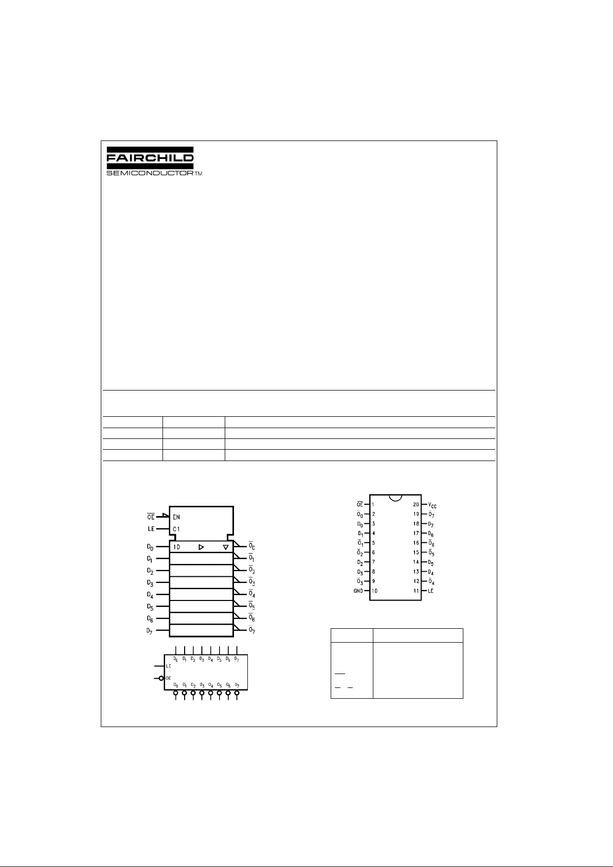
Logic Symbols
IEEE/IEC
Connection Diagram
Pin Descriptions
FACT, FACT Quiet Series, and GTO are trademarks of F airchild Semiconductor Corporation.
Order Number Package Number Package Description
74ACTQ533SC M20B 20-Lead Small Outline Integrated Circuit (SOIC), JEDEC MS-013, 0.300” Wide Body
74ACTQ533MTC MTC20 20-Lead Thin Shrink Small Outline Package (TSSOP), JEDEC MO-153, 4.4mm Wide
74ACTQ533PC N20A 20-Lead Plastic Dual-In-Line Package (PDIP), JEDEC MS-001, 0.300” Wide
Pin Names Description
D
0–D7
Data Inputs
LE Lat ch Enable Input
OE
Output Enable Input
O
0–O7
3-STATE Latch Outputs
Page 2
www.fairchildsemi.com 2
74ACTQ533
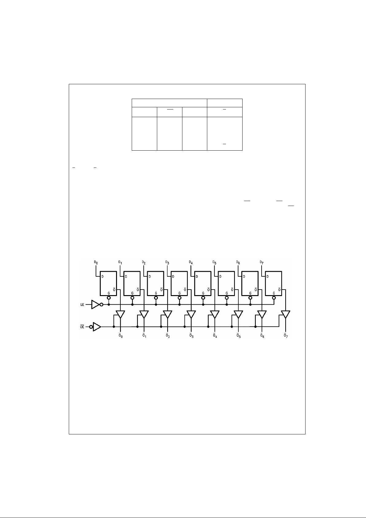
Truth Table
H = HIGH Voltage Level
L = LOW Voltage Level
Z = High Impedance
X = Immaterial
O
0
= Previous O0 before HIGH-to-LOW transition of Latch Enable
Functional Description
The ACTQ533 contains eight D-type latches with 3-STATE
standard outputs. When the Latch Enable (LE) input is
HIGH, data on the D
n
inputs enters the latches. In this con-
dition the latches are transparent, i.e., a la tch output will
change state each time its D input cha nges. When LE is
LOW, the latches store the information that was present on
the D inputs at setup time preceding the HIGH-to-LOW
transition of LE. The 3-STATE standard outputs are controlled by the Output Enab le (O E
) input. When OE is LOW,
the standard outputs are i n the 2-st ate mode. Wh en OE
is
HIGH, the standard outputs are in the high impedance
mode but this does not interfere with entering new data into
the latches.
Logic Diagram
Please note that this diagram is provided only for the understanding of logic operations and should not be used to estimate propagation delays.
Inputs Outputs
LE OE
D
n
O
n
X H X Z
H L L H
H L H L
L L X O
0
Page 3
3 www.fairchildsemi.com
74ACTQ533
Absolute Maximum Ratings(Note 1) Recommended Operating
Conditions
Note 1: Absolute max imum ratings are those values beyond which damage
to the device may occu r. The databook spe cificatio ns shou ld be met, wit hout exception, to ensure that the system de sign is relia ble over its p ower
supply, temperature, and output/input loading variables. Fairchild does not
recommend operation of FACT circuits outside databook specificat ions.
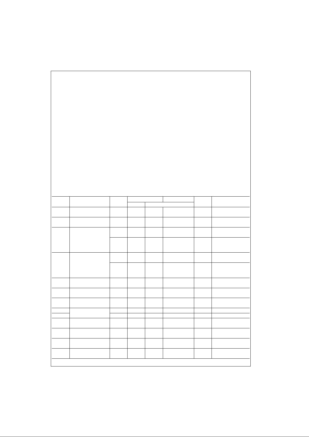
DC Electrical Characteristics
Supply Voltage (VCC) − 0.5V to + 7.0V
DC Input Diode Current (I
IK
)
V
I
= − 0.5V − 20 mA
V
I
= VCC + 0.5V + 20 mA
DC Input Voltage (V
I
) −0.5V to VCC + 0.5V
DC Output Diode Current (I
OK
)
V
O
= − 0.5V − 20 mA
V
O
= VCC + 0.5V + 20 mA
DC Output Voltage (V
O
) − 0.5V to VCC + 0.5V
DC Output Source
or Sink Current (I
O
) ± 50 mA
DC V
CC
or Ground Current
per Output Pin (I
CC
or I
GND
) ± 50 mA
Storage Temperature (T
STG
) − 65°C to + 150°C
DC Latchup Source
or Sink Current ± 300 mA
Junction Temperature (T
J
)
PDIP 140°C
Supply Voltage (V
CC
) 4.5V to 5.5V
Input Voltage (V
I
) 0V to V
CC
Output Voltage (VO) 0V to V
CC
Operating Temperature (TA) −40°C to +85°C
Minimum Input Edge Rate ∆V/∆t 125 mV/ns
V
IN
from 0.8V to 2.0V
V
CC
@ 4.5V, 5.5V
Symbol Parameter
V
CC
TA = +25°C TA = −40°C to +85°C
Units Conditions
(V) Typ Guaranteed Limits
V
IH
Minimum HIGH Level 4.5 1.5 2.0 2.0
V
V
OUT
= 0.1V
Input Voltage 5.5 1.5 2.0 2.0 or VCC − 0.1V
V
IL
Maximum LOW Level 4.5 1.5 0.8 0.8
V
V
OUT
= 0.1V
Input Voltage 5.5 1.5 0.8 0.8 or VCC − 0.1V
V
OH
Minimum HIGH Level 4.5 4.49 4.4 4.4
V I
OUT
= −50 µA
Output Voltage 5.5 5.49 5.4 5.4
V
IN
= V
IL
or V
IH
4.5 3.86 3.76 V IOH = −24 mA
5.5 4.86 4.76 IOH = −24 mA (Note 2)
V
OL
Maximum LOW Level 4.5 0.001 0.1 0.1
V I
OUT
= 50 µA
Output Voltage 5.5 0.001 0.1 0.1
VIN = V
IL
or V
IH
4.5 0.36 0.44 V IOL = 24 mA
5.5 0.36 0.44 I
OL
= 24 mA (Note 2)
I
IN
Maximum Input
5.5 ±0.1 ±1.0 µA VI = VCC, GND
Leakage Current
I
OZ
Maximum 3-STATE
5.5 ±0.25 ±2.5 µA
VI = VIL, V
IH
Leakage Current VO = VCC, GND
I
CCT
Maximum
5.5 0.6 1.5 mA VI = VCC − 2.1V
ICC/Input
I
OLD
Minimum Dynamic 5.5 75 mA V
OLD
= 1.65V Max
I
OHD
Output Current (Note 3) 5.5 −75 mA V
OHD
= 3.85V Min
I
CC
Maximum Quiescent
5.5 4.0 40.0 µA
VIN = V
CC
Supply Current or GND
V
OLP
Quiet Output
5.0 1.1 1.5 V
Figures 1, 2
Maximum Dynamic V
OL
(Note 4)(Note 5)
V
OLV
Quiet Output
5.0 −0.6 −1.2 V
Figures 1, 2
Minimum Dynamic V
OL
(Note 4)(Note 5)
V
IHD
Minimum HIGH Level
5.0 1.9 2.2 V (Note 4)(Note 6)
Dynamic Input Voltage
Page 4
www.fairchildsemi.com 4
74ACTQ533
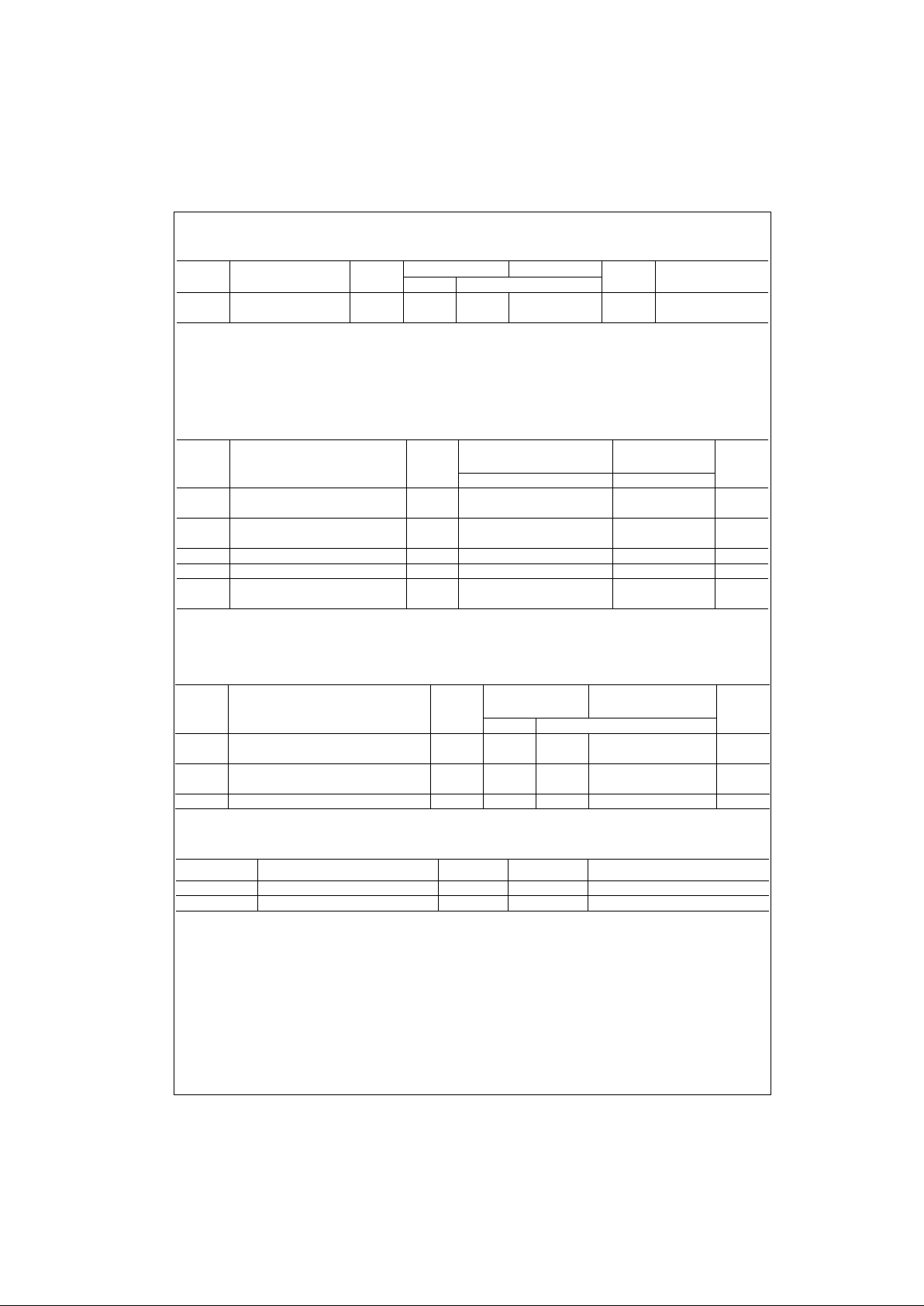
DC Electrical Characteristics (Continued)
Note 2: All outputs loaded; thresholds on input assoc iat ed with output under tes t.
Note 3: Maximum test duratio n 2. 0 ms, one output loaded at a time.
Note 4: DIP package .
Note 5: Max number of output s d ef ined as (n). Data inputs ar e driven 0V to 3V. One output @ GND.
Note 6: Max number of data inputs (n) switching. (n−1) inputs switching 0V to 3V Input-under-test switching: 3V to thre shold (V
ILD
), 0V to threshold (V
IHD
),
f = 1 MHz.
AC Electrical Characteristics
Note 7: Voltage Range 5.0 is 5.0V ± 0.5V.
Note 8: Skew is defined as the absolute value of the difference between the actual propagation delay for any two separate outputs of the same device. The
specification applies to any outputs switchin g in th e s am e direction, either HIGH-t o-LOW (t
OSHL
) or LOW-to-HIGH (t
OSLH
). Parameter guaranteed by design.
AC Operating Requirements
Note 9: Voltage Range 5.0 is 5.0V ± 0.5V.
Capacitance
Symbol Parameter
V
CC
TA = +25°C TA = −40°C to +85°C
Units Conditions
(V) Typ Guaranteed Limits
V
ILD
Maximum LOW Level
5.0 1.2 0.8 V (Note 4)(Note 6)
Dynamic Input Voltage
Symbol Parameter
V
CC
TA = + 25°CT
A
= − 40°C to + 85°C
Units
(V)
C
L
= 50 pF CL = 50 pF
(Note 7) Min Typ Max Min Max
t
PHL
Propagation Delay
5.0 2.0 6.0 8.0 2.0 8.5 ns
t
PLH
Dn to O
n
t
PHL
Propagation Delay
5.0 2.5 7.0 9.0 2.5 9.5 ns
t
PLH
LE to O
n
t
PZL
, t
PZH
Output Enable Time 5.0 2.0 7.0 9.0 2.0 9.5 ns
t
PHZ
, t
PLZ
Output Disable Time 5.0 1.0 8.0 10.0 1.0 10.5 ns
t
OSHL
Output to Output Skew
5.0 0.5 1.0 1.0 ns
t
OSLH
Dn to On(Note 8)
Symbol Parameter
V
CC
TA = + 25°CT
A
= − 40°C to + 85°C
Units
(V)
C
L
= 50 pF CL = 50 pF
(Note 9) Typ Guaranteed Minimum
t
S
Setup Time, HIGH or LOW
5.0 0 3.0 3.0 ns
D
n
to LE
t
H
Hold Time, HIGH or LOW
5.0 0 1.5 1.5 ns
Dn to LE
t
W
LE Pulse Width, HIGH 5.0 2.0 4.0 4.0 ns
Symbol Parameter Typ Units Conditions
C
IN
Input Capacitance 4.5 pF VCC = OPEN
C
PD
Power Dissipation Capacitance 40 pF VCC = 5.0V
Page 5
5 www.fairchildsemi.com
74ACTQ533
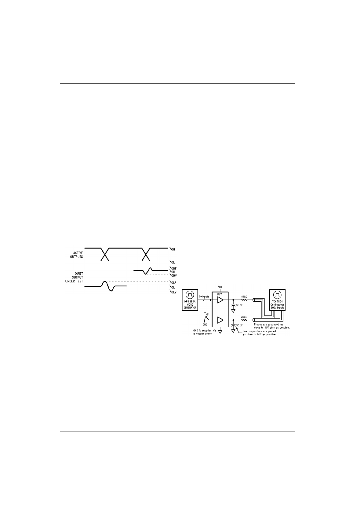
FACT Noise Characteristics
The setup of a noise characteristics measurement is critical
to the accuracy and repeatability of the tests. The following
is a brief description of the setup used to measure the
noise characteristics of FACT.
Equipment:
Hewlett Packard Model 8180A Word Generator
PC-163A Test Fixture Tektronics Model 7854 Oscillo-
scope
Procedure:
1. Verify Test Fixture Loading: Standard Load 50 pF,
500Ω.
2. Deskew the HFS generat or so that no two channels
have greater than 150 ps skew between them. This
requires that the oscilloscope be deskewed first. It is
important to deskew the HFS generator channels
before testing. This will ensure that the outputs switch
simultaneously.
3. Terminate all inputs and outputs to ensure proper loading of the outputs and that the input levels are at the
correct voltage.
4. Set the HFS generator to toggle all but on e outpu t at a
frequency of 1 MHz. Greater frequencies will increase
DUT heating and effect the results of the measurement.
5. Set the HFS gen erator input le vels at 0V LOW and 3V
HIGH for ACT devices and 0V LOW and 5V HIGH for
AC devices. Verify levels with a digital volt meter.
FIGURE 1. Quiet Output Noise Voltage Waveforms
Note 10: V
OHV
and V
OLP
are measured with respect to ground reference.
Note 11: Input pulses have the following cha racteristics:
f = 1 MHz, t
r
= 3ns, tf = 3ns, skew < 150 ps.
V
OLP/VOLV
and V
OHP/V OHV
:
• Determine the quiet output pin that demonstrates the
greatest noise levels. The worst case pin will us ually be
the furthest from th e g rou nd pin . Monitor the output vol tages using a 50Ω coaxial ca ble plug ged i nto a stand ard
SMB type connector on the test fixture. Do not use an
active FET probe.
• Measure V
OLP
and V
OLV
on the quiet output du ring the
worst case transition for active and enable. Measure
V
OHP
and V
OHV
on the quiet output during the worst
case active and enable transition.
• Verify that the GND reference recorded on the oscilloscope has not drifted to ensure the accuracy and repeatability of the measurements.
V
ILD
and V
IHD
:
• Monitor one of the switching outputs using a 50Ω coaxial
cable plugged into a st andard SMB type connector on
the test fixture. Do not use an active FET probe.
• First increase the input LOW voltage level, V
IL
, until the
output begins to oscillate or steps o ut a min of 2 ns.
Oscillation is defined as noise on the output LOW level
that exceeds V
IL
limits, or on output HIGH levels that
exceed V
IH
limits. The input LOW voltage level at which
oscillation occurs is defined as V
ILD
.
• Next decrease the in put HIGH voltage le vel on the V
IH
until the output begins to oscillate or steps out a min of 2
ns. Oscillation is defined as noise on the output LOW
level that exceeds V
IL
limits, or on output HIGH levels
that exceed V
IH
limits. The input HIGH voltage level at
which oscillation occurs is defined as V
IHD
.
• Verify that the GND reference recorded on the oscilloscope has not drifted to ensure the accuracy and repeatability of the measurements.
FIGURE 2. Simultaneous Switching Test Circuit
Page 6
www.fairchildsemi.com 6
74ACTQ533
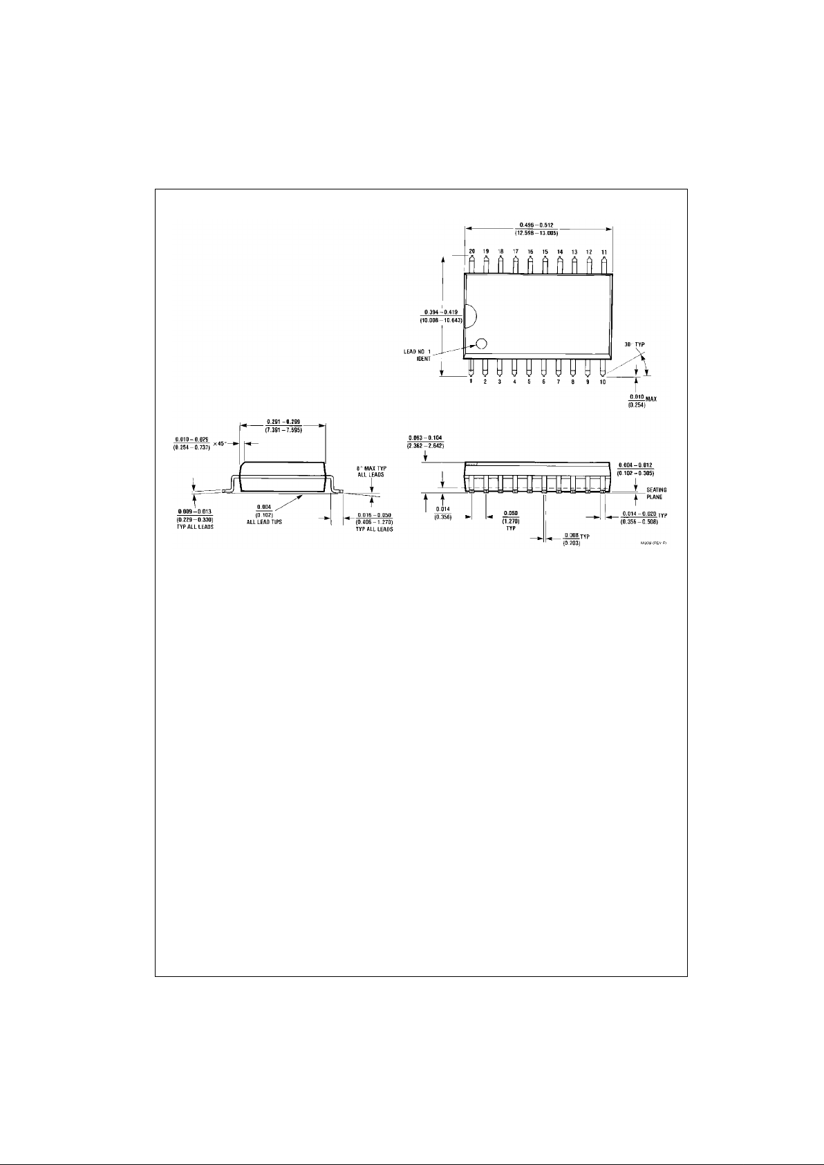
Physical Dimensions inches (millimeters) unless otherwise noted
20-Lead Small Outline Integrated Circuit (SOIC), JEDEC MS-013, 0.300” Wide Body
Package Number M20B
Page 7
7 www.fairchildsemi.com
74ACTQ533
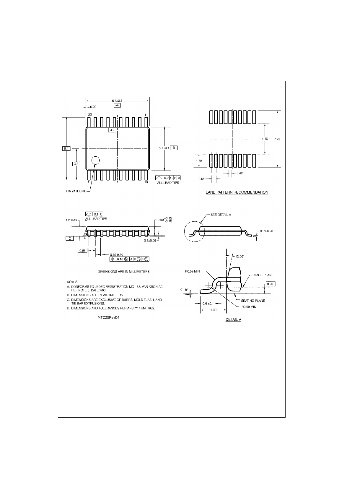
Physical Dimensions inches (millimeters) unless otherwise noted (Continued)
20-Lead Thin Shrink Small Outline Package (TSSOP), JEDEC MO-153, 4.4mm
Package Number MTC20
Page 8
www.fairchildsemi.com 8
74ACTQ533 Quiet Series Octal Transparent Latch with 3-STATE O utputs
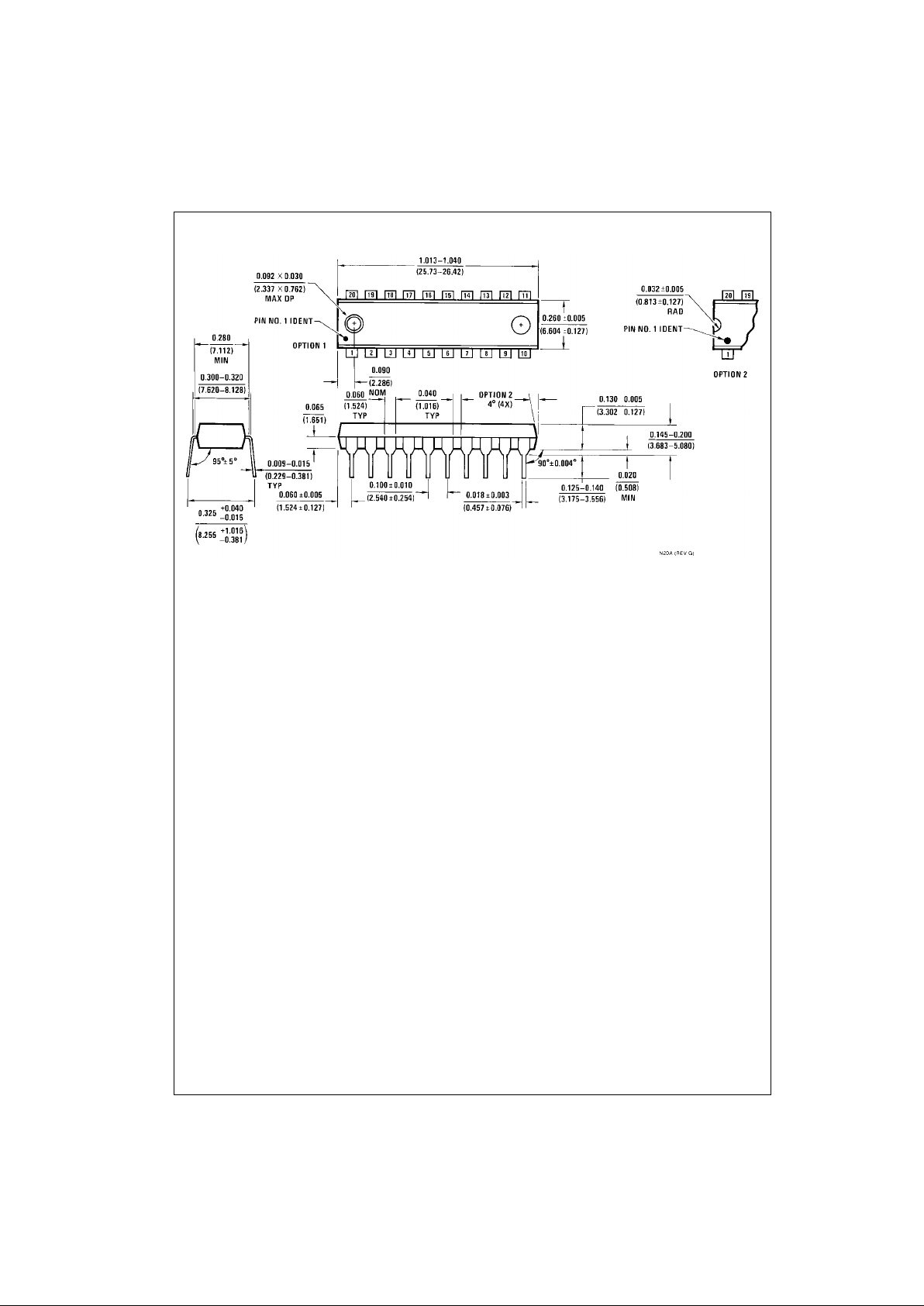
Physical Dimensions inches (millimeters) unless otherwise noted (Continued)
20-Lead Plastic Dual-In-Line Package (PDIP), JEDEC MS-001, 0.300” Wide
Package Number N20A
Fairchild does not assume any responsibility for use of any circuitr y described, no circuit patent licenses are implied and
Fairchild reserves the right at any time without notice to change said circuitry and specifications.
LIFE SUPPORT POLICY
FAIRCHILD’S PRODUCTS ARE NOT AUTHORIZED FOR USE AS CRITICAL COMPONENTS IN LIFE SUPPORT
DEVICES OR SYSTEMS WITHOUT THE EXPRESS WRITTEN APPROVAL OF THE PRESIDENT OF FAIRCHILD
SEMICONDUCTOR CORPORATION. As used herein:
1. Life support devices or systems are devices or syste ms
which, (a) are intended for surgical implant into the
body, or (b) support or sustain life, and (c) whose failure
to perform when properly used in accordance with
instructions for use provided in the labeling, can be reasonably expected to result in a significant inju ry to the
user.
2. A critical component in any compon ent of a lif e supp ort
device or system whose failure t o perform can be reasonably expected to ca use the failure of the life supp ort
device or system, or to affect its safety or effectiveness.
www.fairchildsemi.com
 Loading...