

Datasheet 74ACTQ18823SSCX, 74ACTQ18823SSC, 74ACTQ18823MTDX, 74ACTQ18823MTD, 74ACTQ18823CW Datasheet (Fairchild Semiconductor)
Page 1
© 1999 Fairchild Semiconductor Corporation DS010953 www.fairchildsemi.com
September 1991
Revised November 1999
74ACTQ18823 18-Bit D-Type Flip-Flop with 3-STATE Outputs
74ACTQ18823
18-Bit D-Type Flip-Flop with 3-STATE Outputs
General Description
The ACTQ18823 contains eighteen non-inverting D-type
flip-flops with 3-STATE outputs and is intended for bus oriented applications. The dev ice is byte controlled. A buffered clock (CP), Clear (CLR
), Clock Enable (EN) and
Output Enable (OE
) are common to each byte and can be
shorted together for full 18-bit operation.
The ACTQ18823 utilizes Fairchild’s Quiet Series technol-
ogy to guarantee quiet output switching and improved
dynamic threshold perf ormance. FACT Quiet Series fe atures GTO output control and undersho ot corrector for
superior performance.
Features
■ Utilizes Fairchild’s FACT Quiet Series technology
■ Broadside pinout allows for easy board layout
■ Guaranteed simultan eous switch ing noise level and
dynamic threshold performan ce
■ Guaranteed pin-to-pin output skew
■ Separate control logic for each byte
■ Extra data width for wider address/data p aths or buses
carrying parity
■ Outputs source/sink 24 mA
■ Additional specs for Multiple Output Switching
■ Output loading specs for both 50 pF and 250 pF loads
Ordering Code:
Device also available in Tape and Reel. Specify by appending suffix letter “X” to the ordering code.
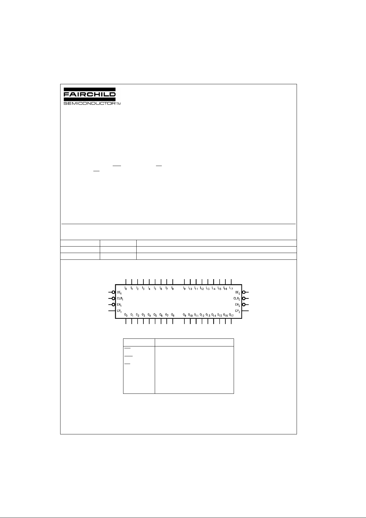
Logic Symbol
Pin Descriptions
FACT, Qui et Series , FACT Quiet Series, an d GTO are trademarks of Fairchild Semiconductor Corporation.
Order Number Package Number Package Description
74ACTQ18823SSC MS56A 56-Lead Shrink Small Outline Package (SSOP), JEDEC MO-118, 0.300” Wide
74ACTQ18823MTD MTD56 56-Lead Thin Shrink Small Outline Package (TSSOP), JEDEC MO-153, 6.1mm Wide
Pin Names Description
OE
n
Output Enable Input (Active LOW)
CLR
n
Clear (Active LOW)
EN
n
Clock Enable (Active LOW)
CP
n
Clock Pulse Input
I
0–I17
Inputs
O
0–O17
Outputs
Page 2
www.fairchildsemi.com 2
74ACTQ18823
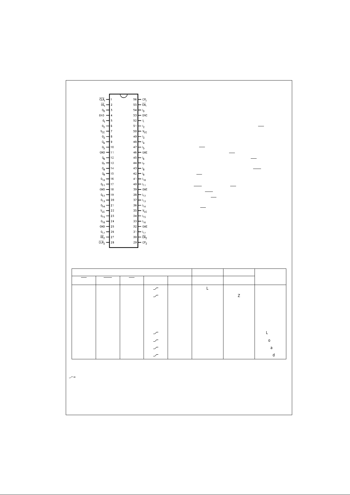
Connection Diagram Functional Description
The ACTQ18823 consists of eighteen D-type edge-triggered flip-flops. These h ave 3-STATE outputs for bus systems organized with inp uts and outpu ts on opposite sides.
The device is byte controlle d with each byte functioning
identically, but independent of the other. The control pins
can be shorted togethe r to ob tain full 16-b it op eration . The
following description applies to each byte. The buffered
clock (CP
n
) and buffered Outpu t Enable (OEn) are com-
mon to all flip-flops within that byte. The flip-flops will store
the state of their indi vidual D inputs that meet set-up and
hold time requir ements on the LOW-to-HIGH CP
n
transi-
tion. With OE
n
LOW, the contents of the flip-flops are avail-
able at the outputs. When OE
n
is HIGH, the outputs go to
the impedance state. Op eration of the OE
n
input does not
affect the state of the flip-flops. In addition to the Clock and
Output Enable pins, there are Clear (CLR
n
) and Clock
Enable (EN
n
) pins. These devices are ide al for parity bus
interfacing in high performance systems.
When CLR
n
is LOW and OEn is LOW, the outputs are
LOW. When CLR
n
is HIGH, data can be entered into the
flip-flops. When EN
n
is LOW, data on the inputs is trans-
ferred to the outputs on the LOW-to-HIGH clock transition.
When the EN
n
is HIGH, the output s do not change state,
regardless of the data or clock input transitions.
Function Table (Note 1)
H= HIGH Voltage Level
L= LOW Voltage Level
X= Immaterial
Z= High Impedance
= LOW-to-HIGH Transition
NC= No Change
Note 1: The table represents t he logic for one byte. The tw o by t es are independent of each other and function ide nt ic ally.
Inputs Internal Output
Function
OE
CLR EN CP I
n
QO
n
HXL
L L Z High Z
HXL
H H Z High Z
HLXXX L Z Clear
LLXXX L L Clear
HHHXX NC Z Hold
LHHXX NC NC Hold
HHL
L L Z Load
HHL
H H Z Load
LHL
L L L Load
LHL
H H H Load
Page 3
3 www.fairchildsemi.com
74ACTQ18823
Logic Diagrams
Byte 1 (0:8)
Byte 2 (9:17)
Page 4

www.fairchildsemi.com 4
74ACTQ18823
Absolute Maximum Ratings(Note 2) Recommended Operating
Conditions
Note 2: Absolute maximum ratings are those values beyond which damage
to the device may occur. The databook specifications should be met, without exception, to ensure that the system design is reliable over its power
supply, temperature, and ou tput/inp ut loadi ng varia bles. Fairchild does no t
recommend operat ion of FACT circuits outside da t abook specifications.
DC Electrical Characteristics
Note 3: All outputs loaded; thresholds associated with output under test.
Note 4: Maximum test duratio n 2. 0 ms, one output loaded at a time.
Note 5: Worst case package.
Note 6: Maximum number of outputs that can switch simultaneously is n. (n − 1) outputs are switched LOW and one output held LOW.
Note 7: Maximum number of outputs that can switch simultaneously is n. (n − 1) out puts are switched HIGH and one output held HIGH.
Note 8: Maximum number of data inputs (n) switching. (n − 1) input switching 0V to 3V. Input under test switching 3V to threshold (V
ILD
).
Supply Voltage (VCC) −0.5V to +7.0V
DC Input Diode Current (I
IK
)
V
I
= −0.5V −20 mA
V
I
= VCC +0.5V +20 mA
DC Output Diode Current (I
OK
)
V
O
= −0.5V −20 mA
V
O
= VCC +0.5V +20 mA
DC Output Voltage (V
O
) −0.5V to VCC + 0.5V
DC Output Source/Sink Current (I
O
) ± 50 mA
DC V
CC
or Ground Current
Per Output Pin ± 50 mA
Junction Temperature
PDIP/SOIC +140°C
Storage Temperature −65°C to +150°C
ESD Last Passing Voltage (Min) 4000V
Supply Voltage (V
CC
) 4.5V to 5.5V
Input Voltage (V
I
) 0V to V
CC
Output Voltage (VO) 0V to V
CC
Operating Temperature (TA) −40°C to +85°C
Minimum Input Edge Rate (∆V/∆t) 125 mV/ns
V
IN
from 0.8V to 2.0V
V
CC
@ 4.5V, 5.5V
Symbol Parameter
V
CC
TA = +25°CTA = −40°C to +85°C
Units Conditions
(V) Typ Guaranteed Limits
V
IH
Minimum HIGH 4.5 1.5 2.0 2.0
V
V
OUT
= 0.1V
Input Voltage 5.5 1.5 2.0 2.0 or VCC −0.1V
V
IL
Maximum LOW 4.5 1.5 0.8 0.8
V
V
OUT
= 0.1V
Input Voltage 5.5 1.5 0.8 0.8 or VCC −0.1V
V
OH
Minimum HIGH 4.5 4.49 4.4 4.4
VI
OUT
= −50 µA
Output Voltage 5.5 5.49 5.4 5.4
VIN = VIL or V
IH
4.5 3.86 3.76 V IOH = −24 mA
5.5 4.86 4.76 I
OH
= −24 mA (Note 3)
V
OL
Maximum LOW 4.5 0.001 0.1 0.1
VI
OUT
= 50 µA
Output Voltage 5.5 0.001 0.1 0.1
VIN = VIL or V
IH
4.5 0.36 0.44 V IOL = 24 mA
5.5 0.36 0.44 IOL = 24 mA (Note 3)
I
OZ
Maximum 3-STATE
5.5 ±0.5 ±5.0 µA
VI = VIL, V
IH
Leakage Current VO = VCC, GND
I
IN
Maximum Input Leakage Current 5.5 ±0.1 ±1.0 µAVI = VCC, GND
I
CCT
Maximum ICC/Input 5.5 0.6 1.5 mA VI = VCC −2.1V
I
CC
Maximum Quiescent Supply Current 5.5 8.0 80.0 µAVIN = VCC or GND
I
OLD
Minimum Dynamic
5.5
75 mA V
OLD
= 1.65V Max
I
OHD
Output Current(Note 4) −75 mA V
OHD
= 3.85V Min
V
OLP
Quiet Output Maximum Dynamic V
OL
5.0 0.5 0.8 V (Note 6)(Note 7)
V
OLV
Quiet Output Minimum Dynamic V
OL
5.0 −0.5 −0.8 V (Note 6)(Note 7)
V
OHP
Maximum Overshoot 5.0 VOH + 1.0 VOH + 1.5 V (Note 5)(Note 7)
V
OHV
Minimum VCC Droop 5.0 VOH − 1.0 VOH − 1.8 V (Note 5)(Note 7)
V
IHD
Minimum High Voltage Level 5.0 1.7 2.0 V (Note 5)(Note 8)
V
ILD
Maximum Low Dynamic Input Voltage Level 5.0 1.2 1.2 V (Note 5)(Note 8)
Page 5

5 www.fairchildsemi.com
74ACTQ18823
AC Electrical Characteristics
Note 9: Voltage Range 5.0 is 5.0V ± 0.5V.
AC Operating Requirements
Note 10: Voltage Ran ge 5.0 is 5.0V ± 0.5V.
V
CC
TA = +25°CT
A
= −40°C to +85°C
Symbol Parameter (V)
C
L
= 50 pF CL = 50 pF
Units
(Note 9) Min Typ Max Min Max
f
MAX
Maximum Clock
5.0 100 90 MHz
Frequency
t
PHL
Propagation Delay 5.0 2.0 9.0 2.0 9.5
ns
t
PLH
CPn to O
n
2.0 9.0 2.0 9.5
t
PHL
Propagation Delay
5.0 2.0 9.0 2.0 9.5 ns
CLRn to O
n
t
PZL
Output Enable Time 5.0 2.0 9.0 2.0 10.0
ns
t
PZH
2.0 9.0 2.0 10.0
t
PLZ
Output Disable Time 5.0 1.5 7.0 1.5 7.5
ns
t
PHZ
1.5 8.0 1.5 8.5
V
CC
TA = +25°CT
A
= −40°C to +85°C
Symbol Parameter (V)
C
L
= 50 pF CL = 50 pF
Units
(Note 10) Typ Guaranteed Minimum
t
S
Setup Time, HIGH or LOW,
5.0 3.0 3.0 ns
Input to Clock
t
H
Hold Time, HIGH or LOW,
5.0 1.5 1.5 ns
Input to Clock
t
S
Setup Time, HIGH or LOW,
5.0 3.0 3.0 ns
Enable to Clock
t
H
Hold Time, HIGH or LOW,
5.0 1.5 1.5 ns
Enable to Clock
t
W
CPn Pulse Width,
5.0 4.0 4.0 ns
HIGH or LOW
t
W
CLRn Pulse Width,
5.0 4.0 4.0 ns
HIGH or LOW
t
REC
Recovery Time,
5.0 6.0 6.0 ns
CLR
n
to CP
n
Page 6

www.fairchildsemi.com 6
74ACTQ18823
Extended AC Electrical Characteristics
Note 11: Skew is defined as the abs olute valu e of th e differenc e betwee n the ac tual p ropagat ion delay s for any two separate output s of the same dev ice.
The specification ap plies to any ou tputs switc hing HIGH -to-LO W (t
OSHL
), LOW-to-HIGH (t
OSLH
), or any combin atio n swit ch ing LO W-to -HIGH an d/or HI GH-
to-LOW (t
OST
).
Note 12: This specification i s gua rant eed bu t not test ed. Th e li mits a pply to pr opaga tion del ays f or all pa ths des cribe d sw itchi ng i n phase (il.e. , all L OW-toHIGH, HIGH-to-LOW, etc.).
Note 13: This specification is gu aranteed but not tested. The lim its represen t propagation de lays with 250 p F load capacitors in place of the 5 0 pF load
capacitors in the standard AC load. This specification pertains to single output switching only.
Note 14: 3-STATE delays are load dominated and have been excluded from the datasheet.
Note 15: The Output Disable Time is dom inated by the RC network (500Ω, 250 pF) on the output and has been excluded from the datasheet.
Capacitance
Symbol Parameter
TA = −40°C to +85°C
Units
V
CC
= Com TA = −40°C to +85°C
C
L
= 50 pF VCC = Com
16 Outputs Switching
CL = 250 pF
(Note 12) (Note 13)
Min Typ Max Min Max
t
PLH
Propagation Delay 5.2 6.5 7.6 7.0 9.8
ns
t
PHL
CPn to O
n
5.3 6.5 7.8 6.8 10.0
t
PHL
Propagation Delay
4.8 5.3 6.2 5.2 7.5 ns
CLR
n
to O
n
t
PZH
Output Enable Time 4.2 4.8 6.5
(Note 14) ns
t
PZL
4.4 5.3 6.0
t
PHZ
Output Disable Time 3.5 4.2 4.8
(Note 15) ns
t
PZL
4.6 5.2 6.0
t
OSHL
Pin to Pin Skew
1.0 ns
(Note 11) CPn to O
n
t
OSLH
Pin to Pin Skew
1.0 ns
(Note 11) CPn to O
n
t
OSHL
Pin to Pin Skew
1.0 ns
(Note 11) CLRn to Output
t
OST
Pin to Pin Skew
1.5 ns
(Note 11) CPn to Output
Symbol Parameter Typ Units Conditions
C
IN
Input Pin Capacitance 4.5 pF VCC = 5.0V
C
PD
Power Dissipation Capacitance 95 pF VCC = 5.0V
Page 7

7 www.fairchildsemi.com
74ACTQ18823
FACT Noise Characteristics
The setup of a noise characteristics measurement is critical
to the accuracy and repeatability of the tests. The following
is a brief description of the setup used to measure the
noise characteristics of FACT.
Equipment:
Hewlett Packard Model 8180A Word Generator
PC-163A Test Fixture
Tektronics Model 7854 Oscilloscope
Procedure:
1. Verify Test Fixture Loading: Standard Load 50 pF,
500Ω.
2. Deskew the HFS generator so that no two channels
have greater than 150 ps skew between them. This
requires that the oscilloscope be deskewed first. It is
important to deskew the HFS generator channels
before testing. This will ensure that the outputs switch
simultaneously.
3. Terminate all inputs and outputs to ensure proper loading of the outputs and that the input levels are at the
correct voltage.
4. Set the HFS gener ator to toggl e all but on e outpu t at a
frequency of 1 MHz. Greater frequencies will increase
DUT heating and affect the results of the measurement.
V
OHV
and V
OLP
are measured with re s pect to ground reference.
Input pulses have th e following characteristics: f = 1MHz, t
r
= 3ns,
t
f
= 3 ns, skew < 150 ps.
FIGURE 1. Quiet Output Noise Voltage Waveforms
5. Set the HF S gen erator in put le vels at 0V LO W and 3V
HIGH for ACT devices and 0V LOW and 5V HIGH for
AC devices. Verify levels with an oscilloscope.
V
OLP/VOLV
and V
OHP/VOHV
:
• Determine the quiet output pin that demonstrates the
greatest noise levels. The worst case pin will us ually be
the furthest from th e g rou nd pin . Monitor the output vol tages using a 50Ω coaxial ca ble plug ged i nto a stand ard
SMB type connector on the test fixture. Do not use an
active FET probe.
• Measure V
OLP
and V
OLV
on the quiet output du ring the
worst case transition for active and enable. Measure
V
OHP
and V
OHV
on the quiet output during the worst
case active and enable transition.
• Verify that the GND reference recorded on the oscilloscope has not drifted to ensure the accuracy and repeatability of the measurements.
V
ILD
and V
IHD
:
• Monitor one of the switching outputs using a 50Ω coaxial
cable plugged into a st andard SMB type connector on
the test fixture. Do not use an active FET probe.
• First increase the input LOW voltage level, V
IL
, until the
output begins to oscillate or steps o ut a min of 2 ns.
Oscillation is defined as noise on the output LOW level
that exceeds V
IL
limits, or on output HIGH levels that
exceed V
IH
limits. The input LOW voltage level at which
oscillation occurs is defined as V
ILD
.
• Next decrease the input HIGH voltage level, V
IH
, until
the output begins to oscillator steps out a min of 2 ns .
Oscillation is defined as noise on the output LOW level
that exceeds V
IL
limits, or on output HIGH levels that
exceed V
IH
limits. The input HIGH voltage level at which
oscillation occurs is defined as V
IHD
.
• Verify that the GND reference recorded on the oscilloscope has not drifted to ensure the accuracy and repeatability of the measurements.
FIGURE 2. Simultaneous Switching Test Circuit
Page 8

www.fairchildsemi.com 8
74ACTQ18823
Physical Dimensions inches (millimeters) unless otherwise noted
56-Lead Shrink Small Outline Package (SSOP), JEDEC MO-118, 0.300” Wide
Package Number MS56A
Page 9

9 www.fairchildsemi.com
74ACTQ18823 18-Bit D-Type Flip-Flop with 3-STATE Outputs
Physical Dimensions inches (millimeters) unless otherwise noted (Continued)
56-Lead Thin Shrink Sm all Ou tline Pa ck age (TS SO P), JE DE C MO-153, 6.1mm Wide
Package Number MTD56
Fairchild does not assume any responsibility for use of any circuitry described , no circuit patent licenses are implied and
Fairchild reserves the right at any time without notice to change said circuitry and specifications.
LIFE SUPPORT POLICY
FAIRCHILD’S PRODUCTS ARE NOT AUTHORIZED FOR USE AS CRITICAL COMPONENTS IN LIFE SUPPORT
DEVICES OR SYSTEMS WITHOUT THE EXPRESS WRITTEN APPROVAL OF THE PRESIDENT OF FAIRCHILD
SEMICONDUCTOR CORPORATION. As used herein:
1. Life support devices or systems are devices or syste ms
which, (a) are intended for surgical implant into the
body, or (b) support or sustain life, and (c) whose failure
to perform when properly used in accordance with
instructions for use provide d in the labe l ing, can be re asonably expected to result in a significant injury to the
user.
2. A critical component in any com ponen t of a life s uppor t
device or system whose failure to perform can be reasonably expected to cause the failure of the l ife support
device or system, or to affect its safety or effectiveness.
www.fairchildsemi.com
 Loading...