

Datasheet 74ACTQ16244SSCX, 74ACTQ16244SSC, 74ACTQ16244MTDX, 74ACTQ16244MTD, 74ACTQ16244CW Datasheet (Fairchild Semiconductor)
Page 1
© 1999 Fairchild Semiconductor Corporation DS010925 www.fairchildsemi.com
May 1991
Revised November 1999
74ACTQ16244 16-Bit Buffer/Line Driver with 3-STATE Outputs
74ACTQ16244
16-Bit Buffer/Line Driver with 3-STATE Outputs
General Description
The ACTQ16244 contains sixteen non-inverting buffers
with 3-STATE outputs designed to be employed as a memory and address driver, clock driver, or bus oriented transmitter/receiver. The device is nibble controlled. Each nibble
has separate 3-STATE control inputs which can be shorted
together for full 16-bit operation.
The ACTQ16244 utiliz es Fairchild’s Quiet Series technology to guarantee quiet output switching and improved
dynamic threshold perf ormance. FACT Quiet Series fe atures GTO output control for superior performance.
Features
■ Utilizes Fairchild’s FACT Quiet Series technology
■ Guaranteed simultaneous switching noise level and
dynamic threshold performan ce
■ Guaranteed pin-to-pin output skew
■ Separate control logic for each byte and nibble
■ 16-bit version of the ACTQ244
■ Outputs source/sink 24 mA
■ Additional specs for multiple output switching
■ Output loading specs for both 50 pF and 250 pF loads
Ordering Code:
Device also available in Tape and Reel. Specify by appending suffix letter “X” to the ordering code.
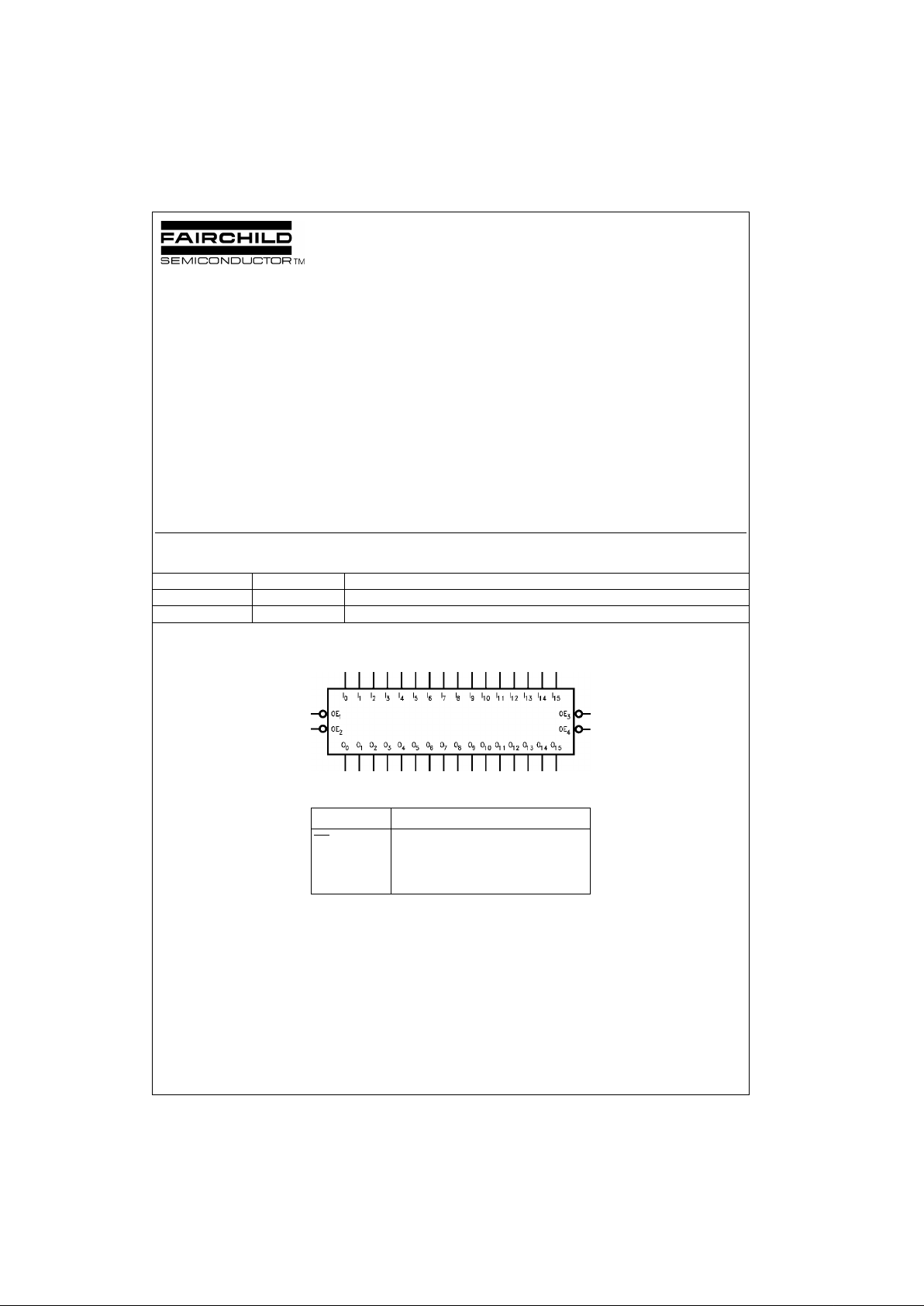
Logic Symbol
Pin Description
FACT, FACT Quiet Series, and GTO are trademarks of F airchild Semiconductor Corporation.
Order Number Package Number Package Description
74ACTQ16244SSC MS48A 48-Lead Small Shrink Outline Package (SSOP), JEDEC MO-118, 0.300” Wide
74ACTQ16244MTD MTD48 48-Lead Thin Shrink Small Outline Package (TSSOP), JEDEC MO-153, 6.1mm Wide
Pin Names Description
OE
n
Output Enable Input (Active LOW)
I
0–I15
Inputs
O
0–O15
Outputs
Page 2
www.fairchildsemi.com 2
74ACTQ16244
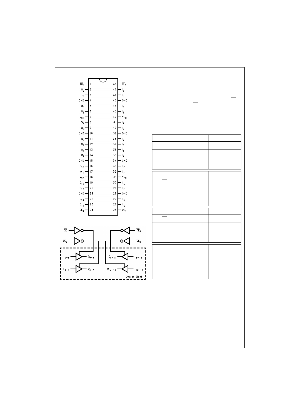
Connection Diagram
Logic Diagram
Functional Description
The ACTQ16244 contains sixteen non-inverting buffers
with 3-STATE standard outputs. The device is nibble
(4 bits) controlled with each nibble functioning ide ntically,
but independent of the other. The control pins can be
shorted together to obtain full 16-bit operation. The 3STAT E outputs are contr olled by an Output E nable (OE
n
)
input for each nibble. When OE
n
is LOW, the outputs are in
2-state mode. Wh en OE
n
is HIGH, the outputs are in the
high impedance mode, but this does not interfere with
entering new data into the inputs.
Tr uth Tables
H = HIGH Voltage Level
L = LOW Voltage Level
X = Immaterial
Z = High Impedance
Inputs Outputs
OE
1
I0–I
3
O0–O
3
LL L
LH H
HX Z
Inputs Outputs
OE
2
I4–I
7
O4–O
7
LL L
LH H
HX Z
Inputs Outputs
OE
3
I8–I
11
O8–O
11
LL L
LH H
HX Z
Inputs Outputs
OE
4
I12–I
15
O12–O
15
LL L
LH H
HX Z
Page 3
3 www.fairchildsemi.com
74ACTQ16244
Absolute Maximum Ratings(Note 1) Recommended Operating
Conditions
Note 1: Absolute max imum rating s are those values beyond w hich damage
to the device may occu r. The databook spe cificatio ns shou ld be met, wit hout exception to ensure that the system design is reliable over its power
supply, temperature, and output/input loading variables. Fairchild does not
recommend operation of FACT circuits outside databook specific at ions.
DC Electrical Characteristics
Note 2: All outputs loaded; thresholds associated with output under test.
Note 3: Maximum test duration 2.0 ms; one output loaded at a time.
Note 4: Worst case package.
Note 5: Maximum number of outputs that can switch simultaneously is n. (n − 1) outputs are switched LOW and one output held LOW.
Note 6: Maximum number of outputs that can switch simultaneously is n. (n − 1) outputs are switched HIGH and one output held HIGH.
Note 7: Max number of data input s (n ) s w it c hing. (n − 1) input switching 0V to 3V input under test switching 3V to threshold (V
ILD
)
Supply Voltage (VCC) −0.5V to +7.0V
DC Input Diode Current (I
IK
)
V
I
= − 0.5V −20 mA
V
I
= VCC + 0.5V +20 mA
DC Output Diode Current (I
OK
)
V
O
= −0.5V −20 mA
V
O
= VCC + 0.5V +20 mA
DC Output Voltage (V
O
) −0.5V to VCC + 0.5V
DC Output Source/Sink Current (I
O
) ±50 mA
DC V
CC
or Ground Current
per Output Pin ±50 mA
Junction Temperature +140°C
Storage Temperature −65°C to +150°C
Supply Voltage (V
CC
) 4.5V to 5.5V
Input Voltage (V
I
)0V to V
CC
Output Voltage (VO)0V to V
CC
Operating Temperature (TA) −40°C to +85°C
Minimum Input Edge Rate (∆V/∆t) 125 mV/ns
V
IN
from 0.8V to 2.0V
V
CC
@ 4.5V, 5.5V
Symbol Parameter
V
CC
TA = +25°C
TA = −40°C to +85°C
Units Conditions
(V) Typ Guaranteed Limits
V
IH
Minimum HIGH 4.5 1.5 2.0 2.0
V
V
OUT
= 0.1V
Input Voltage 5.5 1.5 2.0 2.0 or VCC − 0.1V
V
IL
Maximum LOW 4.5 1.5 0.8 0.8
V
V
OUT
= 0.1V
Input Voltage 5.5 1.5 0.8 0.8 or VCC − 0.1V
V
OH
Minimum HIGH 4.5 4.49 4.4 4.4
VI
OUT
= −50 µA
Output Voltage 5.5 5.49 5.4 5.4
VIN = VIL or V
IH
4.5 3.86 3.76 V IOH = −24 mA
5.5 4.86 4.76 IOH = −24 mA (Note 2)
V
OL
Maximum LOW 4.5 0.001 0.1 0.1
VI
OUT
= 50 µA
Output Voltage 5.5 0.001 0.1 0.1
VIN = VIL or V
IH
4.5 0.36 0.44 V IOH = 24 mA
5.5 0.36 0.44 I
OH
= 24 mA (Note 2)
I
OZ
Maximum 3-STATE
5.5 ± 0.5 ± 5.0 µA
VI = VIL, V
IH
Leakage Current VO = VCC, GND
I
IN
Maximum Input Leakage Current 5.5 ± 0.1 ± 1.0 µAVI = VCC, GND
I
CCT
Maximum ICC/Input 5.5 0.6 1.5 mA VI = VCC −2.1V
I
CC
Max Quiescent Supply Current 5.5 8.0 80.0 µAVIN = VCC or GND (Note 6)
I
OLD
Minimum Dynamic 5.5 75 mA V
OLD
= 1.65V Max
I
OHD
Output Current (Note 3) −75 mA V
OHD
= 3.85V Min
V
OLP
Quiet Output Maximum Dynamic V
OL
5.0 0.5 0.8 V Figure 1, Figure 2
(Note 5)(Note 6)
V
OLV
Quiet Output Minimum Dynamic V
OL
5.0 −0.5 −1.0 V Figure 1, Figure 2
(Note 5)(Note 6)
V
OHP
Maximum Overshoot 5.0 VOH + 1.0 VOH + 1.5 V (Note 4)(Note 6)
V
OHV
Minimum VCC Droop 5.0 VOH − 1.0 VOH − 1.8 V (Note 4)(Note 6)
V
IHD
Minimum HIGH Dynamic Input Voltage Level 5.0 1.7 2.0 V (Note 4)(Note 7)
V
ILD
Maximum LOW Dynamic Input Voltage Level 5.0 1.2 0.8 V (Note 4)(Note 7)
Page 4

www.fairchildsemi.com 4
74ACTQ16244
AC Electrical Characteristics
Note 8: Voltage Range 5.0 is 5.0V ± 0.5V.
Extended AC Electrical Characteristics
Note 9: Voltage Range 5.0 is 5.0V ± 0.5V.
Note 10: Skew is defined as the absolu te valu e of the differe nce bet ween the actu al propag ation de lays for a ny two s eparat e outpu ts of the s ame devic e.
The specification ap plies to any ou tputs switc hing HIGH -to-LO W (t
OSHL
), LOW-to-HIGH (t
OSLH
), or any combin atio n swit ch ing LO W-to -HIGH an d/or HI GH-
to-LOW (t
OST
).
Note 11: This specification is gu aranteed but not tested. The limits apply to propagation delays for all paths des c ribed switching in phase
(i.e., all LOW-to-HIGH, HIGH-to-LOW, etc.).
Note 12: This specification is gu aranteed but not tested. The lim its represen t propagation de lays with 250 p F load capacitors in place of the 5 0 pF load
capacitors in the standard AC load. This specification pertains to single output switching only.
Note 13: 3-STATE delays are load dominated and have been excluded from the datasheet.
Note 14: The Output Disable Time is dom inated by the RC network (500Ω, 250 pF) on the output and has been excluded from the datasheet.
Capacitance
V
CC
TA = +25°CT
A
= −40°C to +85°C
Symbol Parameter (V)
C
L
= 50 pF CL = 50 pF
Units
(Note 8) Min Typ Max Min Max
t
PLH
Propagation 3.0 5.2 7.3 3.0 7.8
ns
t
PHL
Delay An, Bn to Bn, A
n
5.0 2.5 4.8 6.8 2.5 7.3
t
PZH
Output Enable 5.0 2.5 5.0 7.4 2.5 7.9
ns
t
PZL
Time 2.7 4.6 7.5 2.7 8.0
t
PHZ
Output Disable 5.0 2.3 5.0 7.9 2.3 8.2
ns
t
PLZ
Time 2.0 4.6 7.4 2.0 7.9
TA = −40°C to +85°C
C
L
= 50 pF TA = −40°C to +85°C
Symbol Parameter
V
CC
16 Outputs Switching
CL = 250 pF
Units
(V) (Note 11) (Note 12)
(Note 8) Min Typ Max Min Max
t
PLH
Propagation Delay 5.0 4.0 11.6 5.6 14.3
ns
t
PHL
Data to Output 3.4 9.6 4.8 13.1
t
PZH
Output Enable 5.0 3.5 10.1 (Note 13)
ns
t
PZL
Time 3.4 10.0
t
PHZ
Output Disable 5.0 3.6 8.9 (Note 14)
ns
t
PLZ
Time 3.1 8.1
t
OSHL
Pin to Pin Skew
5.0 1.2 ns
(Note 10) HL Data to Output
t
OSLH
Pin to Pin Skew
5.0 2.5 ns
(Note 10) LH Data to Output
t
OST
Pin to Pin Skew
5.0 4.3 ns
(Note 10) LH/HL Data to Output
Symbol Parameter Typ Units Conditions
C
IN
Input Pin Capacitance 4.5 pF VCC = 5.0V
C
PD
Power Dissipation Capacitance 30 pF VCC = 5.0V
Page 5

5 www.fairchildsemi.com
74ACTQ16244
FACT Noise Characteristics
The setup of a noise characteristics measurement is critical
to the accuracy and repeatability of the tests. The following
is a brief description of the setup used to measure the
noise characteristics of FACT.
Equipment:
Hewlett Packard Model 8180A Word Generator
PC-163A Test Fixture
Tektronics Model 7854 Oscilloscope
Procedure:
1. Verify Test Fixture Loading: Standard Load 50pF,
500Ω.
2. Deskew the HFS ge nerator so that no two channels
have greater than 150 ps skew between them. This
requires that the oscilloscope be deskewed first. It is
important to deskew the HFS generator channels
before testing. This will ensure that the outputs switch
simultaneously.
3. Terminate all inputs and outputs to ensure proper loading of the outputs and that the input levels are at the
correct voltage.
4. Set the HFS gener ator to toggle al l but on e outpu t at a
frequency of 1 MHz. Greater frequencies will increase
DUT heating and affect the results of the measurement.
V
OHV
and V
OLP
are measured with re s pect to ground reference.
Input pulses have th e following characteristics: f = 1MHz, t
r
= 3ns,
t
f
= 3 ns, skew < 150 ps.
FIGURE 1. Quiet Output Noise Voltage Waveforms
5. Set the HFS gen erator input le vels at 0V LOW and 3V
HIGH for ACT devices and 0V LOW and 5V HIGH for
AC devices. Verify levels with an oscilloscope.
V
OLP/VOLV
and V
OHP/VOHV
:
• Determine the quiet output pin that demonstrates the
greatest noise levels. The worst case pin will us ually be
the furthest from th e g rou nd pin . Monitor the output vol tages using a 50Ω coaxial ca ble plug ged i nto a stand ard
SMB type connector on the test fixture. Do not use an
active FET probe.
• Measure V
OLP
and V
OLV
on the quiet output du ring the
worst case transition for active and enable. Measure
V
OHP
and V
OHV
on the quiet output during the worst
case active and enable transition.
• Verify that the GND reference recorded on t he oscilloscope has not drifted to ensure the accuracy and repeatability of the measurements.
V
ILD
and V
IHD
:
• Monitor one of the switching outputs using a 50Ω coaxial
cable plugged into a st andard SMB type connector on
the test fixture. Do not use an active FET probe.
• First increase the input LOW voltage level, V
IL
, until the
output begins to oscillate or steps o ut a min of 2 ns.
Oscillation is defined as noise on the output LOW level
that exceeds V
IL
limits, or on output HIGH levels that
exceed V
IH
limits. The input LOW voltage level at which
oscillation occurs is defined as V
ILD
.
• Next decrease the input HIGH voltage level, V
IH
, until
the output begins to osci llate or steps o ut a m in o f 2 ns .
Oscillation is defined as noise on the output LOW level
that exceeds V
IL
limits, or on output HIGH levels that
exceed V
IH
limits. The input HIGH voltage level at which
oscillation occurs is defined as V
IHD
.
• Verify that the GND reference recorded on t he oscilloscope has not drifted to ensure the accuracy and repeatability of the measurements
FIGURE 2. Simultaneous Switching Test Circuit
Page 6

www.fairchildsemi.com 6
74ACTQ16244
Physical Dimensions inches (millimeters) unless otherwise noted
48-Lead Small Shrink Outline Package (SSOP), JEDEC MO-118, 0.300” Wide
Package Number MS48A
Page 7

7 www.fairchildsemi.com
74ACTQ16244 16-Bit Buffer/Line Driver with 3-STATE Outputs
Physical Dimensions inches (millimeters) unless otherwise noted (Continued)
48-Lead Thin Shrink Sm all Ou tline Pa ck age (TS SO P), JE DE C MO-153, 6.1mm Wide
Package Number MTD48
Fairchild does not assume any responsibility for use of any circuitry described , no circuit patent licenses are implied and
Fairchild reserves the right at any time without notice to change said circuitry and specifications.
LIFE SUPPORT POLICY
FAIRCHILD’S PRODUCTS ARE NOT AUTHORIZED FOR USE AS CRITICAL COMPONENTS IN LIFE SUPPORT
DEVICES OR SYSTEMS WITHOUT THE EXPRESS WRITTEN APPROVAL OF THE PRESIDENT OF FAIRCHILD
SEMICONDUCTOR CORPORATION. As used herein:
1. Life support devices or systems are devices or systems
which, (a) are intended for surgical implant into the
body, or (b) support or sustain life, and (c) whose failure
to perform when properly used in accordance with
instructions for use provide d in the labe l ing, can be re asonably expected to result in a significant injury to the
user.
2. A critical component in any compo nent o f a l ife supp ort
device or system whose failure to perform can be reasonably expected to cause the failure of the l ife support
device or system, or to affect its safety or effectiveness.
www.fairchildsemi.com
 Loading...