

Datasheet 74ACTQ04SJX, 74ACTQ04SJ, 74ACTQ04SCX, 74ACTQ04SC, 74ACTQ04PC Datasheet (Fairchild Semiconductor)
...Page 1
© 1999 Fairchild Semiconductor Corporation DS010890 www.fairchildsemi.com
August 1990
Revised November 1999
74ACTQ04 Quiet Series Hex Inverter
74ACTQ04
Quiet Series Hex Inverter
General Description
The ACTQ04 contains six inverters and utilizes Fairchild
Quiet Series technology to guarantee quiet output switching and improved dynamic thre shold performance. FACT
Quiet Series features GTO out put control and undershoot corrector in addition to a split ground bus for superior
ACMOS performance.
Features
■ ICC reduced by 50%
■ Guaranteed simultaneous switching noise level and
dynamic threshold performan ce
■ Improved latch-up immunity
■ Outputs source/sink 24 mA
■ Has TTL-compatible inputs
Ordering Code:
Device also available in Tape and Reel. Specify by appending s uffix let te r “X” to the ordering code.
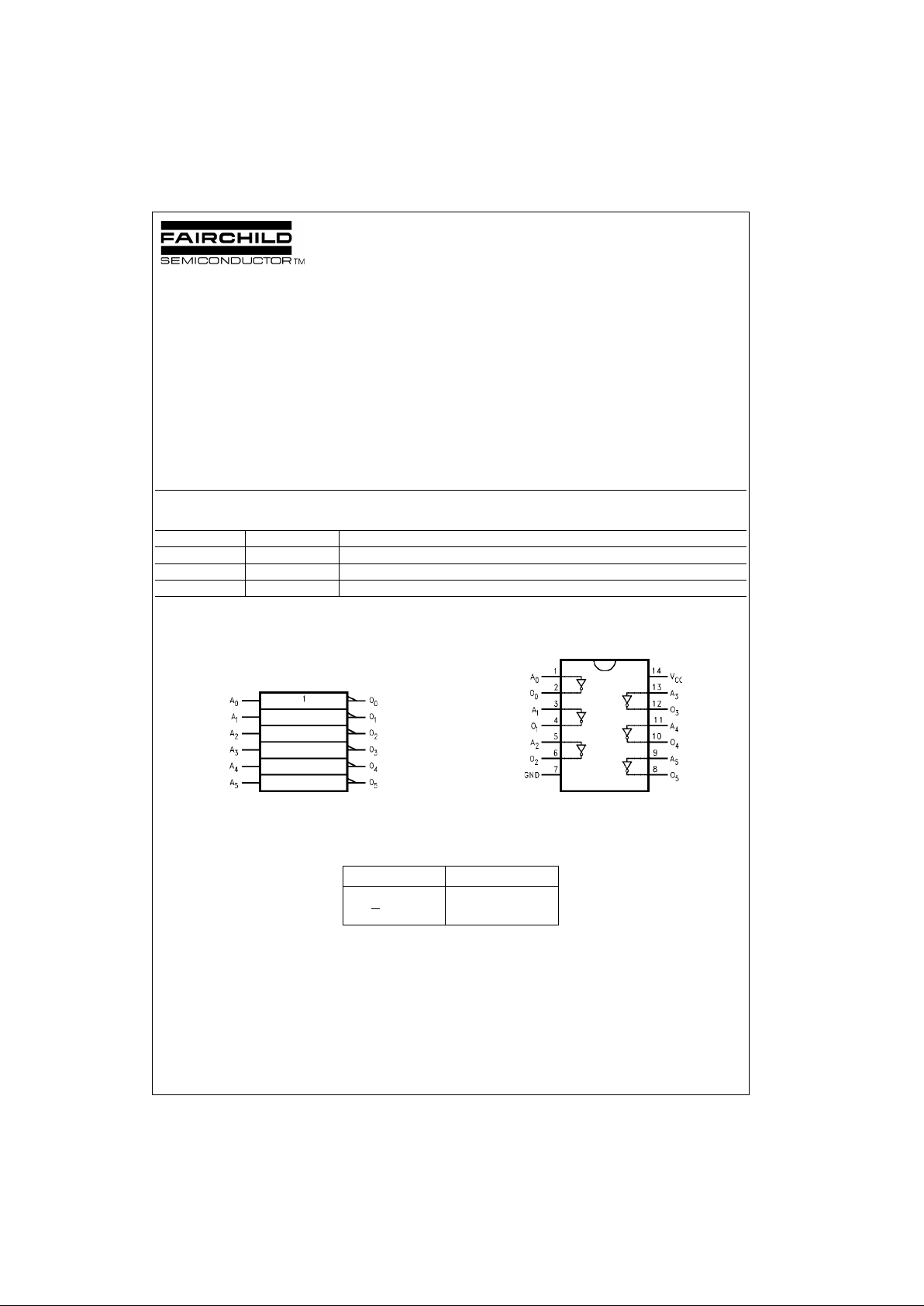
Logic Symbol
IEEE/IEC
Connection Diagram
Pin Descriptions
FACT, Qui et Series , FACT Quiet Series, an d GTO are trademarks of Fairchild Semiconductor Corporation.
Order Number Package Number Package Description
74ACTQ04SC M14A 14-Lead Small Outline Integrated Circuit (SOIC), JEDEC MS-120, 0.150” Narrow Body
74ACTQ04SJ M14D 14-Lead Small Outline Package (SOP), EIAJ TYPE II, 5.3mm Wide
74ACTQ04PC N14A 14-Lead Plastic Dual-In-Line Package (PDIP), JEDEC MS-001, 0.300” Wide
Pin Names Description
A
n
Inputs
O
n
Outputs
Page 2
www.fairchildsemi.com 2
74ACTQ04
Absolute Maximum Ratings(Note 1) Recommended Operating
Conditions
Note 1: Absolute maximum ratings are those values beyond which dam-
age to the device may occu r. The databook specificati ons should be met ,
without exception, t o ensure that the system design is reliab le over its
power supply, temperature, an d output/input loading variables. Fairc hild
does not recommend operation outside of dat abook specifications.
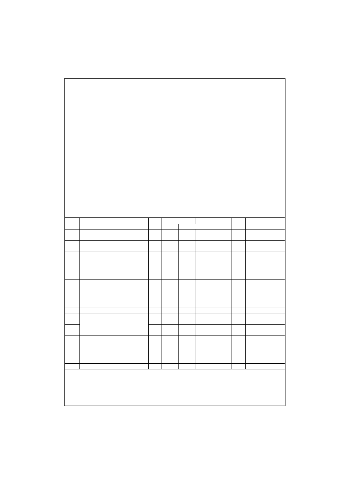
DC Electrical Characteristics for ACTQ
Note 2: All outputs loaded; thresholds on input assoc iat ed with output under tes t.
Note 3: Maximum test duratio n 2. 0 ms, one output loaded at a time.
Note 4: DIP package .
Note 5: Max number of outputs defined as (n). Data inputs are 0V to 3V. One output @ GND.
Note 6: Max number of data inputs (n) switching. (n−1) inputs switching 0V t o 3V Input-under-test swit c hing: 3V to threshold (V
ILD
),
0V to threshold (V
IHD
), f = 1 MHz.
Supply Voltage (VCC) −0.5V to +7.0V
DC Input Diode Current (I
IK
)
V
I
= −0.5V −20 mA
V
I
= VCC + 0.5V +20 mA
DC Input Voltage (V
I
) −0.5V to VCC + 0.5V
DC Output Diode Current (I
OK
)
V
O
= −0.5V −20 mA
V
O
= VCC + 0.5V +20 mA
DC Output Voltage (V
O
) −0.5V to VCC + 0.5V
DC Output Source
or Sink Current (I
O
) ±50 mA
DC V
CC
or Ground Current
per Output Pin (I
CC
or I
GND
) ± 50 mA
Storage Temperature (T
STG
) −65°C to +150°C
DC Latch-up Source
or Sink Current ± 300 mA
Junction Temperature (T
J
)
PDIP 140°C
Supply Voltage (V
CC
) 4.5V to 5.5V
Input Voltage (V
I
) 0V to V
CC
Output Voltage (VO) 0V to V
CC
Operating Temperature (TA) −40°C to +85°C
Minimum Input Edge Rate (∆V/∆t) 125 mV/ns
V
IN
from 0.8V to 2.0V
V
CC
@ 4.5V, 5.5V
Symbol Parameter
V
CC
TA = +25°C TA = −40°C to +85°C
Units Conditions
(V) Typ Guaranteed Limits
VIHMinimum HIGH Level 4.5 1.5 2.0 2.0
V
V
OUT
= 0.1V
Input Voltage 5.5 1.5 2.0 2.0 or VCC − 0.1V
VILMaximum LOW Level 4.5 1.5 0.8 0.8
V
V
OUT
= 0.1V
Input Voltage 5.5 1.5 0.8 0.8 or VCC − 0.1V
VOHMinimum HIGH Level 4.5 4.49 4.4 4.4
V I
OUT
= −50 µA
Output Voltage 5.5 5.49 5.4 5.4
V
IN
= VILor V
IH
4.5 3.86 3.76 V IOH = −24 mA
5.5 4.86 4.76 IOH = −24 mA (Note 2)
V
OL
Maximum LOW Level 4.5 0.001 0.1 0.1
V I
OUT
= 50 µA
Output Voltage 5.5 0.001 0.1 0.1
VIN = VILor V
IH
4.5 0.36 0.44 V IOL = 24 mA
5.5 0.36 0.44 I
OL
= 24 mA (Note 2)
I
IN
Maximum Input Leakage Current 5.5 ± 0.1 ± 1.0 µA VI = VCC, GND
I
CCT
Maximum ICC/Input 5.5 0.6 1.5 mA VI = VCC − 2.1V
I
OLD
Minimum Dynamic 5.5 75 mA V
OLD
= 1.65V Max
I
OHD
Output Current (Note 3) 5.5 −75 mA V
OHD
= 3.85V Min
I
CC
Maximum Quiescent Supply Current 5.5 2.0 20.0 µA VIN = VCC or GND
V
OLP
Quiet Output Maximum Dynamic V
OL
5.0 1.1 1.5 V Figure 1, Figure 2
(Note 4)(Note 5)
V
OLV
Quiet Output Minimum Dynamic V
OL
5.0 −0.6 −1.2 V Figure 1, Figure 2
(Note 4)(Note 5)
V
IHD
Minimum HIGH Level Dynamic Input Voltage 5.0 1.9 2.2 V (Note 4)(Note 6)
V
ILD
Maximum LOW LevelDynamic Input Voltage 5.0 1.2 0.8 V (Note 4)(Note 6)
Page 3
3 www.fairchildsemi.com
74ACTQ04
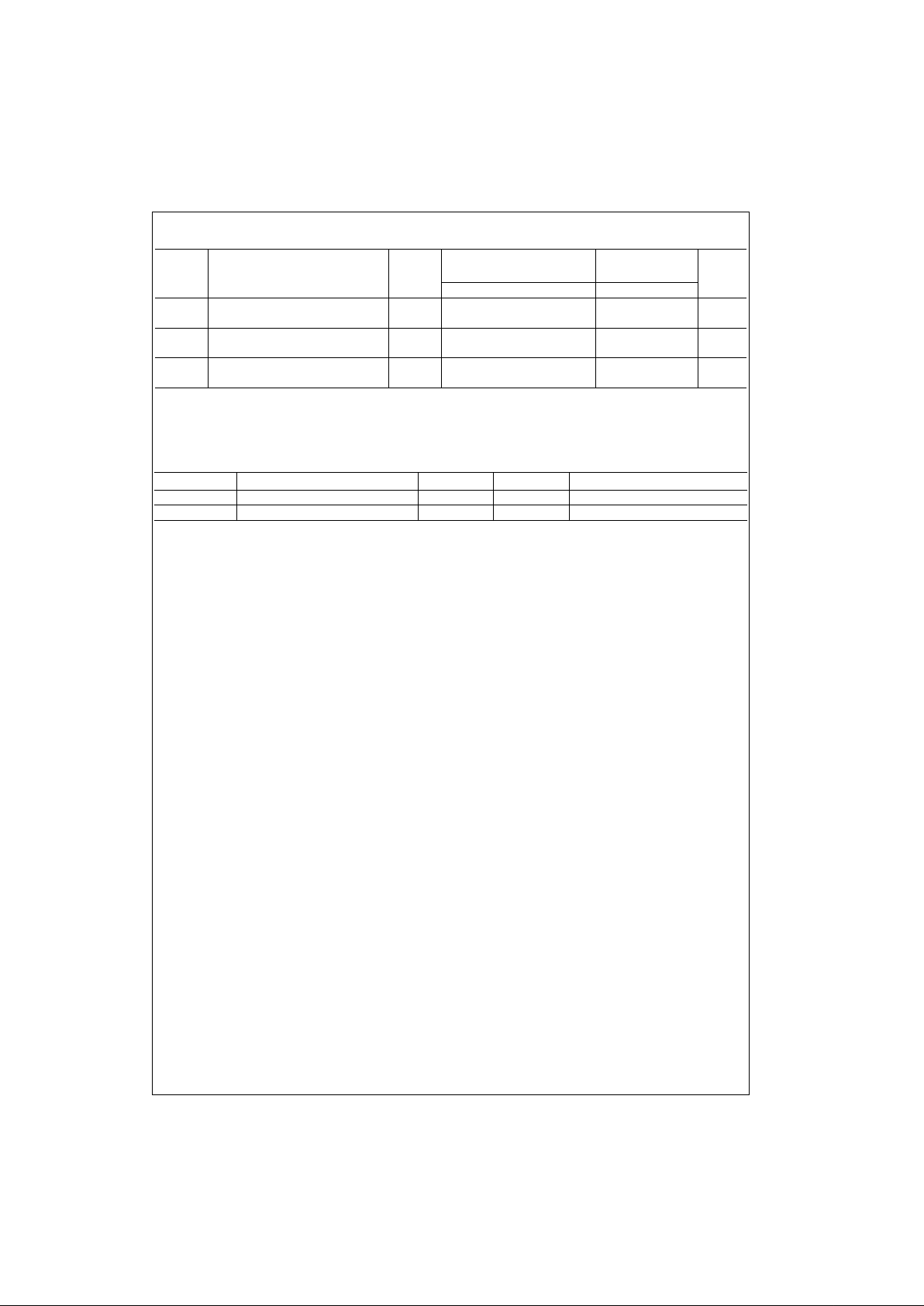
AC Electrical Characteristics
Note 7: Voltage Range 5.0 is 5.0V ± 0.5V.
Note 8: Skew is defined as t he absolute value of t he difference between the actual propagation delay for any two separate outputs of the same device. The
specification applies t o any outputs switching in th e s am e direction, either HIG H to LOW (t
OSHL
) or LOW to HIGH (t
OSLH
). Parameter guaranteed by design.
Capacitance
V
CC
TA = +25°C T
A
= −40°C to +85°C
Symbol Parameter (V)
C
L
= 50 pF CL = 50 pF
Units
(Note 7) Min Typ Max Min Max
t
PLH
Propagation Delay
5.0 2.0 6.5 7.5 2.0 8.0 ns
Data to Output
t
PHL
Propagation Delay
5.0 2.0 6.5 7.5 2.0 8.0 ns
Data to Output
t
OSHL
Output to Output
5.0 0.5 1.0 1.0 ns
t
OSLH
Skew (Note 8)
Symbol Parameter Typ Units Conditions
C
IN
Input Capacitance 4.5 pF VCC = OPEN
C
PD
Power Dissipation Capacitance 75 pF VCC = 5.0V
Page 4
www.fairchildsemi.com 4
74ACTQ04
FACT Noise Characteristics
The setup of a noise characteristics measurement is critical
to the accuracy and repeatability of the tests. The following
is a brief description of the setup used to measure the
noise characteristics of FACT.
Equipment:
Hewlett Packard Model 8180A Word Generator
PC-163A Test Fixture
Tektronics Model 7854 Oscilloscope
Procedure:
1. Verify Test Fixture Loading: Standard Load 50 pF,
500Ω.
2. Deskew the HFS generator so that no two channels
have greater than 15 0 ps skew between them. This
requires that the oscilloscope be deskewed first. It is
important to deskew the HFS generator channels
before testing. This will ensure that the outputs sw itch
simultaneously.
3. Terminate all inputs and outputs to ens ure pro per load ing of the outputs a nd that the input levels a re at the
correct voltage.
4. Set the HFS ge nerato r to togg le all bu t one out put at a
frequency of 1 MHz. Greater fre quencies will increa se
DUT heating and effect the results of the measurement.
V
OHV
and V
OLP
are measured with respect to ground reference.
Input pulses have the fol lowing characteristics: f = 1 MHz, t
r
= 3ns, tf =
3 ns, skew < 150 ps.
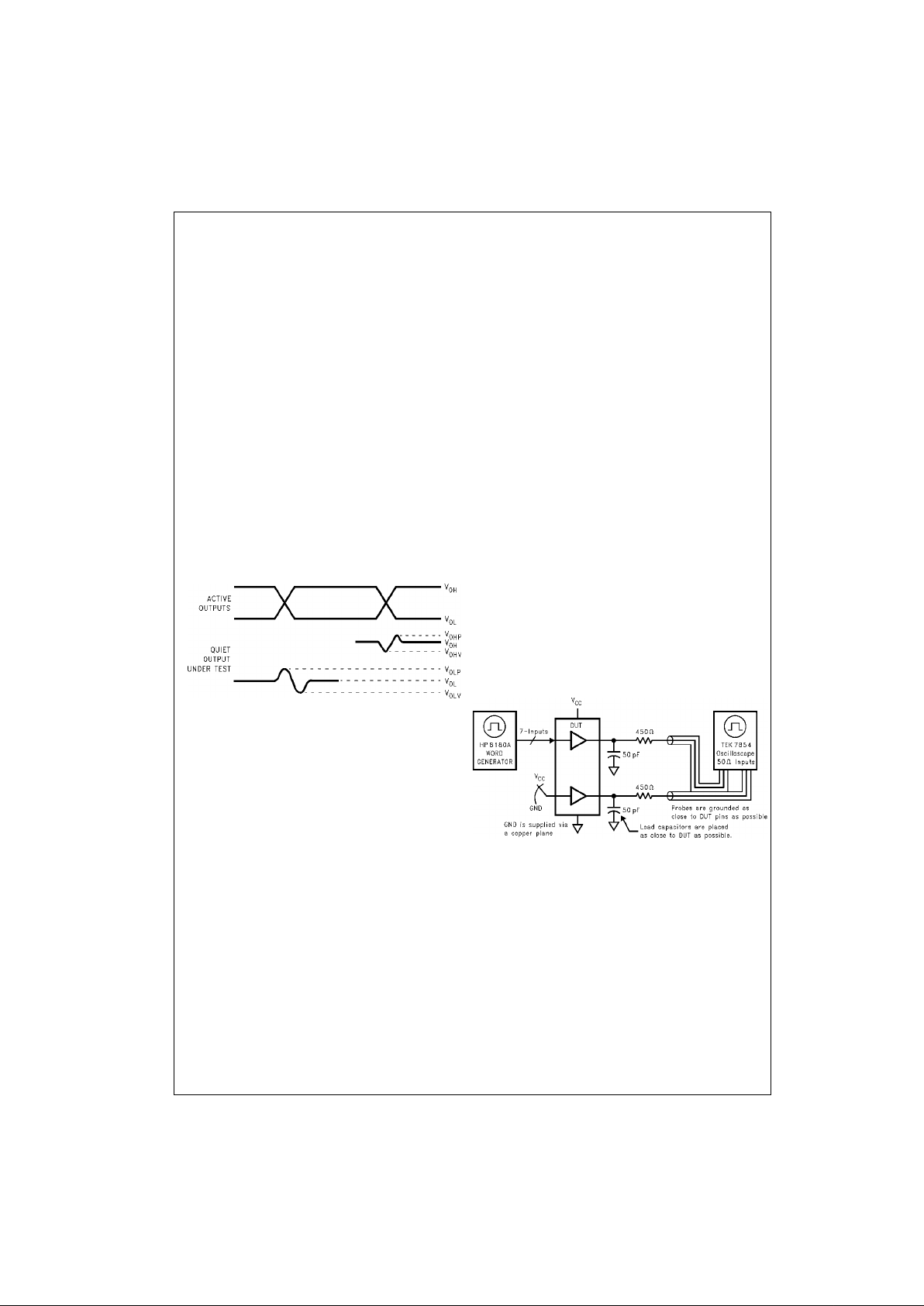
FIGURE 1. Quiet Output Noise Voltage Waveforms
5. Set the HFS gene rator input lev els at 0V LOW a nd 3V
HIGH for ACT devices and 0V LOW and 5V HIGH for
AC devices. Verify levels with an oscilloscope.
V
OLP/VOLV
and V
OHP/V OHV
:
• Determine the quiet output pin that demonstrates the
greatest noise levels. The worst case pin will usually be
the furthest from the gr ound pin. Monitor th e o utp ut voltages using a 50Ω coaxi al cable p lugg ed into a standa rd
SMB type connector on the te st fixture. Do not use an
active FET probe.
• Measure V
OLP
and V
OLV
on the quiet output during the
worst case transition for active and enable. Measure
V
OHP
and V
OHV
on the quiet output during the worst
case transition.for active and enable
• Verify t hat the GND reference recorded on the oscilloscope has not drifted to ensure the accuracy and repeatability of the measurements.
V
ILD
and V
IHD
:
• Monitor one of the switching outputs using a 50Ω coaxial
cable plugged into a standard SMB type connec tor on
the test fixture. Do not use an active FET probe.
• First increase the input LOW voltage level , V
IL
, until the
output begins to oscillate or steps ou t a min of 2 ns.
Oscillation is defined as noise on the output LOW level
that exceeds V
IL
limits, or on output HIGH levels that
exceed V
IH
limits. The input LOW voltage level at which
oscillation occurs is defined as V
ILD
.
• Next decrease the input HIGH voltage level, V
IH
, until
the output begins to oscillate or step s out a min of 2 ns.
Oscillation is defined as noise on the output LOW level
that exceeds V
IL
limits, or on output HIGH levels that
exceed V
IH
limits. The input HIGH voltage level at which
oscillation occurs is defined as V
IHD
.
• Verify t hat the GND reference recorded on the oscilloscope has not drifted to ensure the accuracy and repeatability of the measurements.
FIGURE 2. Simultaneous Switching Test Circuit
Page 5
5 www.fairchildsemi.com
74ACTQ04
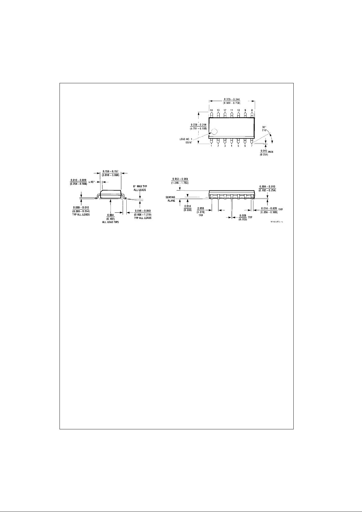
Physical Dimensions inches (millimeters) unless otherwise noted
14-Lead Small Outline Integrated Circuit (SOIC), JEDEC MS-120, 0.150” Narrow Body
Package Number M14A
Page 6
www.fairchildsemi.com 6
74ACTQ04
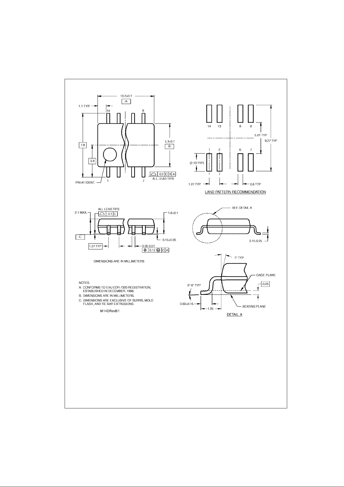
Physical Dimensions inches (millimeters) unless otherwise noted (Continued)
14-Lead Small Outline Package (SOP), EIAJ TYPE II, 5.3mm Wide
Package Number M14D
Page 7
7 www.fairchildsemi.com
74ACTQ04 Quiet Series Hex Inverter
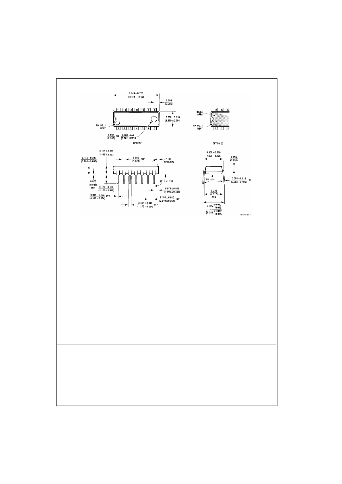
Physical Dimensions inches (millimeters) unless otherwise noted (Continued)
14-Lead Plastic Dual-In-Line Packag e (PDIP), JED EC MS-001, 0.300” Wide
Package Number N14A
Fairchild does not assume any responsibility for use of any circuitry described , no circuit patent licenses are implied and
Fairchild reserves the right at any time without notice to change said circuitry and specifications.
LIFE SUPPORT POLICY
FAIRCHILD’S PRODUCTS ARE NOT AUTHORIZED FOR USE AS CRITICAL COMPONENTS IN LIFE SUPPORT
DEVICES OR SYSTEMS WITHOUT THE EXPRESS WRITTEN APPROVAL OF THE PRESIDENT OF FAIRCHILD
SEMICONDUCTOR CORPORATION. As used herein:
1. Life support devices or systems are dev ic es or syste ms
which, (a) are intended for surgical implant into the
body, or (b) support or sustain life, and (c) whose failure
to perform when properly used in accordance with
instructions for use provide d in the labe l ing, can be re asonably expected to result in a significant injury to the
user.
2. A critical compo nent in any com ponen t of a life s upp ort
device or system whose failure to perform can be reasonably expected to cause the failure of the l ife support
device or system, or to affect its safety or effectiveness.
www.fairchildsemi.com
 Loading...