

Datasheet 74ACT715SCX, 74ACT715SC, 74ACT715RSCX, 74ACT715RSC, 74ACT715RPC Datasheet (Fairchild Semiconductor)
...Page 1
November 1988
Revised December 1998
74ACT715•74ACT715-R Programmable Video Sync Generator
© 1999 Fairchild Semiconductor Corporation DS010137.prf www.fairchildsemi.com
74ACT715•74ACT715-R
Programmable Video Sync Generator
General Description
The ACT715 and ACT715-R are 20-pin TTL-input compatible devices capable of generating Horizontal, Vertical and
Composite Sync and Blank signals for televisions and
monitors. All pulse widths are completely definable by the
user. The devices are capable of generating signals for
both interlaced and noninterlaced modes of operation.
Equalization and serra tion pulses can be introduced into
the Composite Sync signal when needed.
Four additional signals can also be made available when
Composite Sync or Bl ank are used. These sign als can be
used to generate horizontal or vertical gating pulses, cursor
position or vertical Interrupt signal.
These devices make no assumptions concernin g the system architecture. Line rate and field/frame rate are all a
function of the values programme d into the data registers,
the status register, and the input clock frequency.
The ACT715 is mask pr ogrammed to default to a Clock
Disable state. Bit 10 of the Status Register, Register 0,
defaults to a logic “0”. This facilitates (re)programming
before operation.
The ACT715-R is the same as th e ACT715 in all respects
except that the ACT715-R is m ask programmed to default
to a Clock Enabled state. Bit 10 of the Status Register
defaults to a logic “1”. Although completely (re)programmable, the ACT715-R version is be tter suite d for application s
using the default 14.31818 MHz RS-170 register values.
This feature allows power-up directly into operati on, following a single CLEAR pulse.
Features
■ Maximum Input Clock Frequency > 130 MHz
■ Interlaced and non-interlaced formats available
■ Separate or compo site horizontal and vertical Sync and
Blank signals available
■ Complete control of pulse width via register
programming
■ All inputs are TTL compatible
■ 8 mA drive on all outputs
■ Default RS170/NTSC values mask programmed into
registers
■ ACT715-R is mask programm ed to default to a Clock
Enable state for easier start-up into 14.31818 MHz
RS170 timing
Ordering Code:
Device also available in Tape and Reel. Specify by appendin g s uf f ix let t er “X” to the ordering co de.
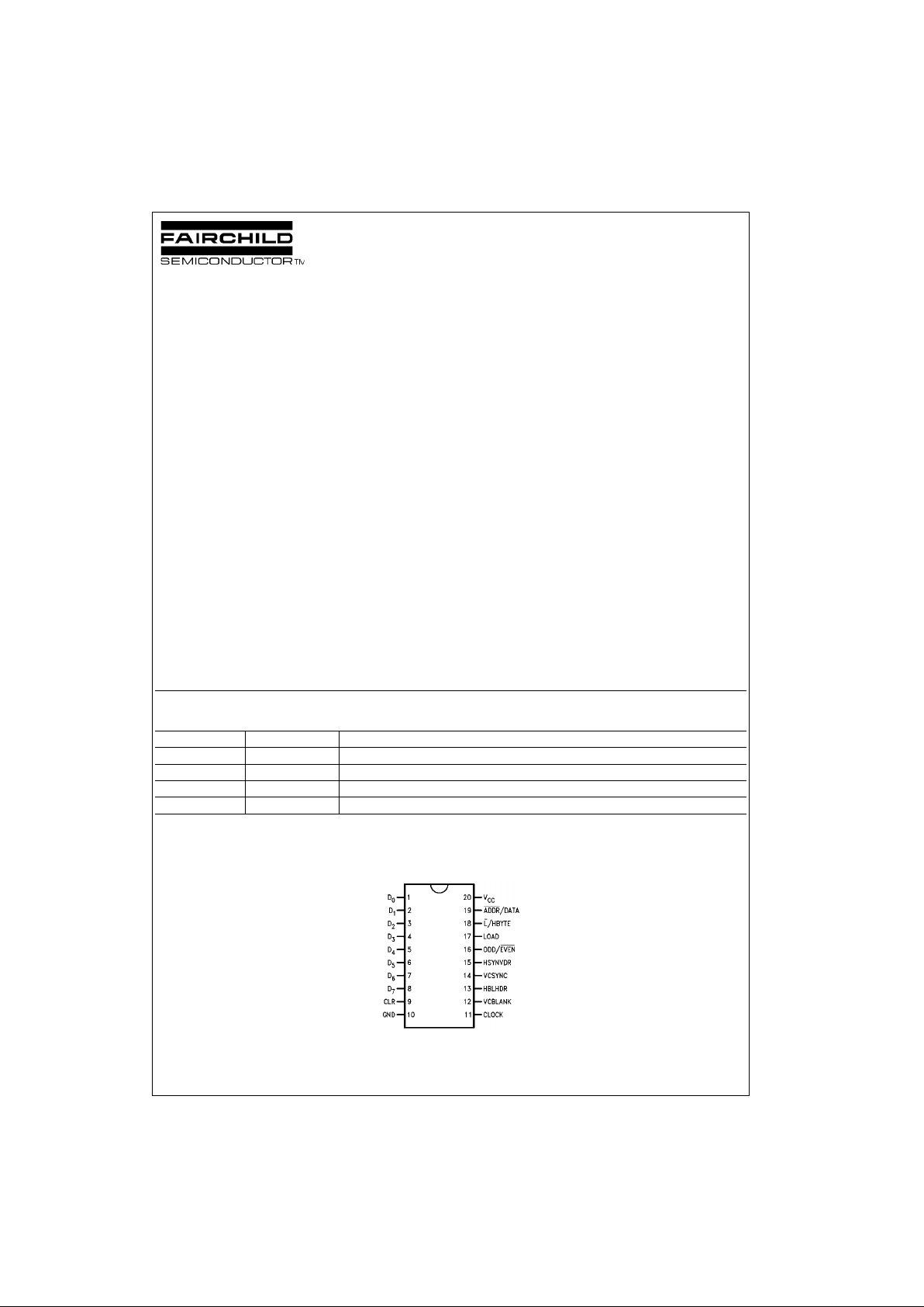
Connection Diagram
Pin Assignment for DIP and SOIC
FACT is a tra demark of Fairchild Semico nductor Corporat ion.
Order Number Package Number Package Description
74ACT715SC M20B 20-Lead Small Outline Integrated Circuit (SOIC), JEDEC MS-013, 0.300” Wide
74ACT715PC N20A 20-Lead Plastic Dual-In-Line Package (PDIP), JEDEC MS-001, 0.300” Wide
74ACT715-RSC M20B 20-Lead Small Outline Integrated Circuit (SOIC), JEDEC MS-013, 0.300” Wide
74ACT715-RPC N20A 20-Lead Plastic Dual-In-Line Package (PDIP), JEDEC MS-001, 0.300” Wide
Page 2
www.fairchildsemi.com 2
74ACT715•74ACT715-R
Logic Block Diagram
Pin Description
There are a Total of 13 inputs and 5 outputs on the
ACT715.
Data Inputs D0–D7: The Data Inp ut pins connect to the
Address Register and the Data Input Register.
ADDR
/DATA: The ADDR/DATA signal is l atched into the
device on the falling edge of the LOAD signal. The sign al
determines if an address (0) or data (1) is present on the
data bus.
L
/HBYTE: The L/HBYTE signal is latched into the device
on the falling edge of the LOAD signal. The signal determines if data will be read into the 8 LSB’s (0) or the 4
MSB’s (1) of the Data Registers. A 1 on this pin when an
ADDR/DATA is a 0 enables Auto-Load Mode.
LOAD: The LOAD control pin lo ads data into the Address
or Data Registers on the rising edge. AD DR
/DATA and L/
HBYTE data is loaded into the device on the falling edge of
the LOAD. The LOAD pin has been implemented as a
Schmitt trigger input for better noise immunity.
CLOCK: System CLOCK input from which all timing is
derived. The clock pin ha s be en i mp leme nte d a s a S chm i tt
trigger for better noise immunity. The CLOCK and the
LOAD signal are asynch ronous and independent. Outp ut
state changes occur on the falling edge of CLOCK.
CLR: The CLEAR pin is an asyn chrono us inp ut that init ializes the device when it is HIGH. Initialization consists of
setting all registe rs to their mask programme d values, and
initializing all counters, comparators and registers. The
CLEAR pin has been impleme nted as a Schmitt tr igger for
better noise immunity. A CLEAR pulse should be ass er ted
by the user immediately after power-u p to ensure proper
initialization of the registers—even if the user plans to
(re)program the device.
Note: A CLEAR p ulse will disable the CLO CK on the ACT715 and will
enable the CLOCK on th e ACT715-R.
ODD/EVEN: Output that identifies if display is in odd
(HIGH) or even (LOW) field of interlace whe n device is in
interlaced mode of operation. In noninterlaced mode of
operation this output is a lways HIGH. Data can be seria lly
scanned out on this pin during Scan Mode.
VCSYNC: Outputs Vertical or Composite Sync signal
based on value of the Status Register. Equalization a nd
Serration pulses will (if enabled) be output on the VCSYNC
signal in composite mode only.
VCBLANK: Outputs Vertical or Composite Blanking signal
based on value of the Status Register.
HBLHDR: Outputs Horizontal Blanking signal, Horizonta l
Gating signal or Cursor Position based on value of the Status Register.
HSYNVDR: Outputs Hori zontal Sync signal, Vertical Gating signal or Vertical Interrupt signal based on value of Status Register.
Page 3
3 www.fairchildsemi.com
74ACT715•74ACT715-R
Register Description
All of the data registers are 12 bits wide. Width’s of all
pulses are defined by specifying the star t count and end
count of all pulses. Horizont al pulses are specified withrespect-to the number o f clock pulses per lin e and ver tical
pulses are specified with-respect-to the number of lines per
frame.
REG0—STATUS REGISTER
The Status Register con trols the mode of operation, the
signals that are output and the polarity of these outputs.
The default value for the Status Registe r is 0 ( 000 Hex) for
the ACT715 and is “1024” (400 Hex) for the ACT715-R.
Bits 0–2
Bits 3–4
Double Equalization and Serration mode will output equ alization and serration puls es at twi ce th e HS YNC fre que ncy
(i.e., 2 equalization or serration pulses for every HSYNC
pulse). Single Equalization and Serration mode will output
an equalization or serra tion pulse for every HSYNC pulse.
In Interlaced mode equalization and serration pulses will be
output during th e VBLANK period of every odd and even
field. Interlaced Single Equaliz ation an d Serrat ion mode is
not possible with this part.
Bits 5–8
Bits 5 through 8 con trol the po larit y of the ou tputs. A value
of zero in these bit locations indicates an output pulse
active LOW. A value of 1 indicates an active HIGH pulse.
B5— VCBLANK Polarity
B6— VCSYNC Polarity
B7— HBLHDR Polarity
B8— HSYNVDR Polarity
Bits 9–11
Bits 9 through 11 enable several different features of the
device.
B9— Enable Equalization/Serration Pulses (0)
Disable Equalization/Serration Pulses (1)
B10— Disable System Clock (0)
Enable System Clock (1)
Default values for B10 are “0” in the ACT715
and “1” in the ACT715-R.
B11— Disable Counter T est Mode (0)
Enable Counter Test Mode (1)
This bit is not intended for the user but is for
internal testing only.
HORIZONTAL INTERVAL REGISTERS
The Horizontal Inter val Registers deter mine the number of
clock cycles per line and the characteristics of the Horizontal Sync and Blank pulses.
REG1— Horizontal Front Porch
REG2— Horizontal Sync Pulse End Time
REG3— Horizontal Blanking Width
REG4— Horizontal Interval Width # of Clocks
per Line
VERTICAL INTERVAL REGISTERS
The Vertical Interval Re gisters determine the number of
lines per f r am e, an d t he ch aracteristics o f t he Vertical B la nk
and Sync Pulses.
REG5— Vertical Front Porch
REG6— Vertical Sync Pulse End Time
REG7— Vertical Blanking Width
REG8— Vertical Interval Width # of Lines
per Frame
EQUALIZATION AND SERRATION PULSE
SPECIFICATION REGISTERS
These registers determine the width of equalization and
serration pulses an d the vertical interval over w hich they
occur.
REG 9— Equalization Pulse Width End Time
REG10— Serration Pulse Width End Time
REG11— Equalization/Serration Pulse Vertical
Interval Start Time
REG12— Equalization/Serration Pulse Vertical
Interval End Time
VERTICAL INTERRUPT SPECIFICATION REGISTERS
These Registers dete rmine the width of the Vertical Interrupt signal if used.
REG13— Vertical Interrupt Activate Time
REG14— Vertical Interrupt Deactivate Time
CURSOR LOCATION REGISTERS
These 4 registers determine the cursor position location, or
they generate separate Horizontal an d Vertical Gati ng signals.
REG15— Horizontal Cursor Position Start Time
REG16— Horizontal Cursor Position End Time
REG17— Vertical Cursor Position Start Time
REG18— Vertical Cursor Position End Time
B
2 B1 B0
VCBLANK VCSYNC HBLHDR HSYNVDR
0 0 0 CBLANK CSYNC HGATE VGATE
(DEFAULT)
0 0 1 VBLANK CSYNC HBLANK VGATE
0 1 0 CBLANK VSYNC HGATE HSYNC
0 1 1 VBLANK VSYNC HBLANK HSYNC
1 0 0 CBLANK CSYNC CUSOR VINT
1 0 1 VBLANK CSYNC HBLANK VINT
1 1 0 CBLANK VSYNC CUSOR HSYNC
1 1 1 VBLANK VSYNC HBLANK HSYNC
B
4B3
Mode of Operation
0 0 Interlaced Double Serration and
(DEFAULT)
Equalization
0 1 Non Interlaced Double Serration
1 0 Illegal State
1 1 Non Interlaced Single Serration and Equalization
Page 4
www.fairchildsemi.com 4
74ACT715•74ACT715-R
Signal Specification
HORIZONTAL SYNC AND BLANK
SPECIFICATIONS
All horizontal si gnals are define d by a star t and end time.
The start and end times are specified in number of clock
cycles per line. The start of the horizontal line is considered
pulse 1 not 0. A ll values of the horizont al timing registers
are referenced to the falling edge of the Hori zontal Blank
signal (see Figure 1). Since the first CLOCK edge, CLOCK
#1, causes the first falling edge of the Horizontal Blank re f-
erence pulse, edges referenced to this first Horizontal edge
are n + 1 CLOCKs away, where “n” is the width of the tim-
ing in question. Registers 1, 2, an d 3 are programmed in
this manner. The horizontal counters start at 1 and count
until HMAX. The value of HMAX must be divisible by 2.
This limitation is imposed beca use durin g interlace operation this value is internally divided by 2 in order to generate
serration and equalizati on pulses at 2 × the horizontal frequency. Horizontal signals will change on the falling edge
of the CLOCK signal. Signal specifications are shown
below.
FIGURE 1. Horizontal Waveform Specificatio n
Horizontal Period (HPER) = REG(4) × ckper
Horizontal Blanking Width: = [REG(3) − 1] × ckper
Horizontal Sync Width: = [REG(2) − REG(1)] × ckper
Horizontal Front Porch: = [REG(1) − 1] × ckper
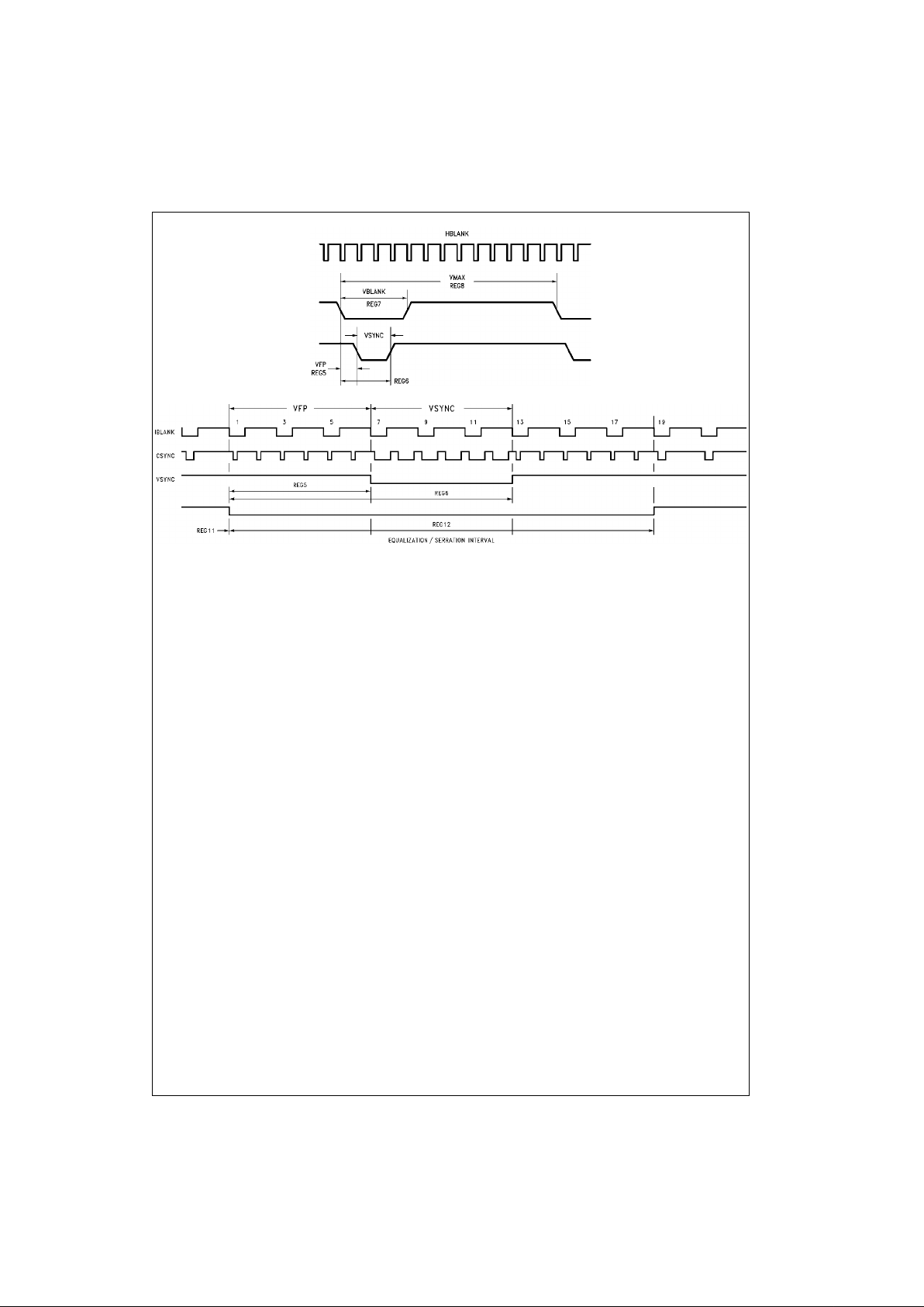
VERTICAL SYNC AND BLANK SPECIFICATION
All vertical sig nals are defi ned in ter ms of numbe r of lines
per frame. This is tr ue i n bo th interlaced and non inte r l ace d
modes of operation. Care must be taken to not s pecify the
Vertical Registers in term s of lines p er field. Sin ce the fir st
CLOCK edge, CLOCK #1, causes the first falling edge of
the Vertical Blank (first Hor izontal Blank) reference pulse,
edges referenced to this fir st edge are n + 1 line s away,
where “n” is the width of the timing in question. Registers 5,
6, and 7 are pr ogramm ed i n th is m an ner. Also, in the in ter laced mode, vertical timing is based on half-lines. Therefore registers 5, 6, and 7 must contain a value twice the
total horizontal (odd and even) plus 1 (as described
above). In non-interlaced mode, all vertical timing is based
on whole-lines. Register 8 is always based on whole-lines
and does not add 1 for the fi rst clock. The vertica l counte r
starts at the value of 1 and counts until the value of VMAX.
No restrictions exist o n the values placed in the vertical
registers. Vertical Blank will change on the leading edge of
HBLANK. Vertical Sync will change on the leading edge of
HSYNC. (See Figure 2.) Vertical Frame Period (VPER) =
REG(8) × hper
Vertical Field Period (VPER/n) = REG(8) × hper/n
Vertical Blanking Width = [REG(7) − 1] × hper/n
Vertical Syncing Width = [REG(6) − REG(5)] × hper/n
Vertical Front Porch = [REG(5) − 1] × hper/n
where n = 1 for noninterlaced
n = 2 for int erlaced
COMPOSITE SYNC AND BLANK SPECIFICATION
Composite Sync and Bl ank sign al s are cr eat ed by lo gica lly
ANDing (ORing) the active LOW (HIG H) sig nal s o f th e co rresponding vertical and horizontal components of these
signals. The Composite Sync signal may also inclu de serration and/or equalization pulses. The Serration pulse interval occurs in place of the Vertical Sync interval.
Equalization pulses occur preceding and/or following the
Serration pulses. The width and location of these p ulses
can be programmed throug h the registers shown below.
(See Figure 3.)
Horizontal Equalization PW = [REG(9) − REG(1)] × ckper
REG 9 = (HFP) + (HEQP) + 1
Horizontal Serration PW: = [REG(4)/n + REG(1) −
REG(10)] × ckper
REG 10 = (HFP) + (HPER/2) − (HSERR) + 1
Where n = 1 for nonint erlaced s ingle serra tion/equ al-
ization
n = 2 for noninterlaced double serration/equal-
ization
n = 2 for interlaced operation
Page 5
5 www.fairchildsemi.com
74ACT715•74ACT715-R
FIGURE 2. Vertical Waveform Specification
FIGURE 3. Equalization/Serration Interval Programming
HORIZONTAL AND VERTICAL GATING SIGNALS
Horizontal Drive and Vertical Drive outputs can be ut ilized
as general purpo se Gati n g S ign al s. Hor i zont al and Vertical
Gating Signals are available for use when Co mp osi te Sync
and Blank signals are selected and the value of Bit 2 of the
Status Register is 0. The Vertical Gating signal will change
in the same manner as that specified for the Vertical Blank.
Horizontal Gating Signal Width = [REG(16) − REG(15)] ×
ckper
Vertical Gating Si gnal Width: = [REG(18) − REG(17)] ×
hper
CURSOR POSITION AND VERTICAL INTERRUPT
The Cursor Position and Vertical Interrupt si gnal are available when Composite Sync an d B lank signals are selected
and Bit 2 of the Status Register is set to the value of 1. The
Cursor Position generates a single pulse of n clocks wide
during every line that the cursor is specified. The signals
are generated by logically ORing (ANDing) the active LOW
(HIGH) signals specified by the regist ers used for generating Horizontal and Vertical Gating signals. The Vertical
Interrupt signal generates a pulse du ring th e verti cal int erval specified. The Vertical Interrupt signal will change in the
same manner as that specified for the Vertical Blanking signal.
Horizontal Cursor Width = [R EG(16) − REG(15)] × ckper
Vertical Cursor Width = [REG(18) − REG(17)] × hper
Vertical Interrupt Width = [REG(14) − REG(13)] × hper
Page 6

www.fairchildsemi.com 6
74ACT715•74ACT715-R
Addressing Logic
The register addressing logic is compo sed of two blocks of
logic. The first is the address register and counter
(ADDRCNTR), and the second is the address decode
(ADDRDEC).
ADDRCNTR LOGIC
Addresses for the data registe rs can be gene rated by one
of two methods. Manual addressing requires that each byte
of each register that needs to be loaded needs to be
addressed. To load both bytes of all 19 registers would
require a total of 57 loa d cycles (19 address and 3 8 data
cycles). Auto Addressing requires that only the initial register value be specified. The Auto Load sequence would
require only 39 load cycles to completely program all registers (1 address and 38 data cycles). In the auto load
sequence the low order byte of the data register will be
written first followed by the high order byte on the next load
cycle. At the time the High Byte is written the address
counter is increment ed by 1. The counter has been implemented to loop on the initial value loaded in to the add ress
register. For example: If a value of 0 was written into the
address register then the cou nter wo uld cou nt fr om 0 to 18
before resetting back to 0. If a value of 15 was wr itten into
the address register th en the count er would count f rom 15
to 18 before looping back to 15. If a value greater than or
equal to 18 is placed into the addr ess register the coun ter
will continuously loop on this value. Auto addressing is initiated on the falling edge of LOAD when ADDRDATA is 0
and LHBYTE is 1. Incre menting an d load ing of data registers will not commence until the falling edge of LOAD after
ADDRDATA goes to 1. The next rising edge of LOAD will
load the first byte of data. Auto Incrementing is disabled on
the falling edge of LOAD after ADDRDATA and LHBYTE
goes low.
Manual Addressing Mode
Auto Addressing Mode
Cycle # Load Falling Edge Load Rising Edge
1 Enable Manual Addressing Load Address m
2 Enable Lbyte Data Load Load Lbyte m
3 Enable Hbyte Data Load Load Hbyte m
4 Enable Manual Addressing Load Address n
5 Enable Lbyte Data Load Load Lbyte n
6 Enable Hbyte Data Load Load Hbyte n
Cycle # Load Falling Edge Load Rising Edge
1 Enable Auto Addressing Load Start Addre ss n
2 Enable Lbyte Data Load Load Lbyte (n )
3 Enable Hbyte Data Load Load Hbyte (n); Inc Counter
4 Enable Lbyte Data Load Load Lbyte (n+1)
5 Enable Hbyte Data Load Load Hbyte (n+1); Inc Counter
6 Enable Manual Addressing Load Address
Page 7

7 www.fairchildsemi.com
74ACT715•74ACT715-R
ADDRDEC LOGIC
The ADDRDEC logic decodes the current address and
generates the enable signal for the appropriate register.
The enable values for the registers a nd counters change
on the falling edge of LOAD. Two types of ADDRDEC logic
is enabled by 2 pair of addresses, Addresses 22 or 54
(Vectored Restart logic) and Addresses 23 or 55 (Vectored
Clear logic). Loading these addresses will enable the
appropriate logic an d put the par t into eithe r a Restar t (all
counter registers are reinitialized with preprogrammed
data) or Clear (all registers are cleared to zero) state.
Reloading the same ADDRDEC address will not cause any
change in the state of the part. The outputs during these
states are frozen and the internal CLOCK is disabled.
Clocking the part during a Vectored Restar t or Vectored
Clear state will have no effect on the part. To resume operation in the new state, or disable th e Vectored Restart or
Vectored Clear state, another non-ADDRDEC address
must be loaded. Operation will begin in the new state on
the rising edge of the non-ADDRDEC loa d pulse. It is recommended that an unused ad dr ess b e loaded following an
ADDRDEC operation to prevent data registers from accidentally being corrupted. The following Addresses are
used by the device.
Address 0 Status Register REG0
Address 1–18Data Registers REG1–REG18
Address 19–21Unused
Address 22/54Restart Vector (Restarts Device)
Address 23/55Clear Vector (Zeros All Registers)
Address 24–31Unused
Address 32–50Register Scan Addresses
Address 51–53Counter Scan Addr esse s
Address 56–63Unused
At any given time only one register at most is selected. It is
possible to have no registers selected.
VECTORED RESTART ADDRESS
The function of addresses 22 (16H) or 54 ( 36H ) ar e si m il ar
to that of the CLR pin except that the preprogramming of
the registers is not affected. It is recommended but not
required that this address is read after the initial device
configuration load sequence. A 1 on the ADDRDATA pin
(Auto Addressing Mode) will not cause this address to
automatically increment. The address will loop back onto
itself regardless of the state of ADDRDATA unless the
address on the Data inputs has been changed with
ADDRDATA at 0.
VECTORED CLEAR ADDRESS
Addresses 23 (17H) or 55 (37H) is used to clear a ll registers to zero simultaneously. This function may be desirable
to use prior to loading n ew data into the Data or Status
Registers. This address is re ad into th e device in a similar
fashion as all of the other registers. A 1 on the ADDRDATA
pin (Auto Addressing Mode) will not cause this address to
automatically increment. The address will loop back onto
itself regardless of the state of ADDRDATA unless the
address on the Data inputs has been changed with
ADDRDATA at 0.
FIGURE 4. ADDRDEC Timing
GEN LOCKING
The ACT715 and ACT715- R is desi gned for maste r S YNC
and BLANK signal ge neration. However, the devices can
be synchronized (slaved) to an exter nal timing signal in a
limited sense. Using Vectored Restart, the user can reset
the counting sequen ce to a given location, the beginning,
at a given time, the rising edge of the LOAD tha t removes
Vector Restart. At this time the next CLOCK pulse will be
CLOCK 1 and the count will resta r t at th e beginn ing of the
first odd line.
Preconditioning the part during normal operat ion, before
the desired synchronizing pulse, is necessary. However,
since LOAD and CLOCK ar e asynchronous and ind ependent, this is possible without interruption or data and performance corruption. If t he defaulted 14.31818 M Hz RS-170
values are being used, precondition ing and restarting can
be minimized by using the CLEAR pulse instead of the
Vectored Restart operation. The ACT715 -R is better suited
for this application because it eliminates the need to p rogram a 1 into Bit 10 of th e Status Register to en able the
CLOCK. Gen Locking to another co unt locati on other t han
the very beginning or separa te horizontal/ver tical resetting
is not possible with the ACT715 nor the ACT715-R.
SCAN MODE LOGIC
A scan mode is available i n the ACT715 that allows the
user to non-destruct ively verify the contents of the registers. Scan mode is invoked through reading a scan
address into the add ress register. The scan address of a
given register is define d by the Da ta reg i ster ad dress + 32.
The internal Clocking signal is disabled when a scan
address is read. Di sabling the clock freezes the device in
it's present state. Data can t hen b e ser ia lly scanne d out o f
the data registers through the ODD/EVEN Pin. The LSB
will be scanned out first. Since each register is 12 bits wide,
completely scanning out data of the addressed register will
require 12 CLOCK pulses. More than 12 CLOCK pulses on
the same register will only cause the MS B to r epeat on the
output. Re-scanning the same register will require that register to be reloaded. The value of the two horizontal
counters and 1 vertical counter can also be scanned out by
using address numbers 51 –53. Note that before the part
will scan out the data, the LOAD signal must b e brought
back HIGH.
Normal device operation ca n be resumed by loading in a
non-scan address. As the scanning of the registers is a
non-destructive scan, the device will resume correct operation from the point at which it was halted.
Page 8

www.fairchildsemi.com 8
74ACT715•74ACT715-R
RS170 Default Register V alues
The tables below show the values programmed for the
RS170 Format (using a 14.31818 MHz clock signal) and
how they compare against the actual EIA RS170 Specifications. The default signals that will be output are CSYNC,
CBLANK, HDRIVE and VDRIVE. The device initially starts
at the beginning of the odd field of interlace. All signals
have active low pulses and the clock is disabled at power
up. Registers 13 and 14 are no t involved in the actu al signal information. If the Vertical Interrupt was selected so that
a pulse indicating the active lines would be output.
RS170 Horizontal Data
Reg D Value H Register Description
REG0 0 000 Status Register (715)
REG0 1024 400 Status Register (715-R)
REG1 23 017 HFP End Time
REG2 91 05B HSYNC Pulse End Time
REG3 157 09D HBLANK Pulse End Time
REG4 910 38E Total Horizontal Clocks
REG5 7 007 VFP End Time
REG6 13 00D VSYNC Pulse End Time
REG7 41 029 VBLANK Pulse End Time
REG8 525 20D Total Vertical Lines
REG9 57 039 Equalization Pulse End Time
REG10 410 19A Serration Pulse Start Time
REG11 1 001 Pulse Interval Start Time
REG12 19 013 Pulse Interval End Time
REG13 41 029 Vertical Interrupt Activate Time
REG14 526 20E Vertical Interrupt Deactivate Time
REG15 911 38F Horizontal Drive Start Time
REG16 92 05C Horizontal Drive End Time
REG17 1 001 Vertical Drive Start Time
REG18 21 015 Vertical Drive End Time
Rate Period
Input Clock 14.31818 MHz 69.841 ns
Line Rate 15.73426 kHz 63.556 µs
Field Rate 59.94 Hz 16.683 ms
Frame Rate 29.97 Hz 33.367 ms
Signal Width µs %H Specification (µs)
HFP 22 Clocks 1.536 1.5 ±0.1
HSYNC Width 68 Clocks 4.749 7.47 4.7 ±0.1
HBLANK Width 156 Clocks 10.895 17.15 10.9 ±0.2
HDRIVE Width 91 Clocks 6.356 10.00 0.1H ±0.005H
HEQP Width 34 Clocks 2.375 3.74 2.3 ±0.1
HSERR Width 68 Clocks 4.749 7.47 4.7 ±0.1
HPER iod 910 Clocks 63.556 100
RS170 Vertical Data
VFP 3 Lines 190.67 6 EQP Pulses
VSYNC Width 3 Lines 190.67 6 Serration Pulses
VBLANK Width 20 Lines 1271.12 7.62 0.075V ± 0.005V
VDRIVE Width 11.0 Lines 699.12 4.20 0.04V ± 0.006V
VEQP Intrvl 9 Lines 3.63 9 Lines/Field
VPERiod (field) 262.5 Lines 16.683 ms 16.683 ms/Field
VPERiod (frame) 525 Lines 33.367 ms 33.367 ms/Frame
Page 9

9 www.fairchildsemi.com
74ACT715•74ACT715-R
Absolute Maximum Ratings(Note 1)
Recommended Operating
Conditions
Note 1: Absolute maximum ratings are those values beyond which damage
to the device may occur. The databook specifications should be met, without exception, to ensure that the system design is reliable over its power
supply, temperature and outpu t/input load ing variables. Fairchild d oes not
recommend operat ion of FACT circuits outside databook specifications.
DC Electrical Characteristics
For ACT Family Devices over Operating Temperature Range (unless otherwise specified)
Note 2: All outputs loaded; thresholds on input associated with in put under test.
Note 3: Test Load 50 pF, 500Ω to Ground .
Supply Voltage (VCC) −0.5V to +7.0V
DC Input Diode Current (I
IK
)
V
I
= −0.5V −20 mA
V
I
= VCC +0.5V +20 mA
DC Input Voltage (V
I
) −0.5V to V
CC
+0.5V
DC Output Diode Current (I
OK
)
V
O
= −0.5V −20 mA
V
O
= VCC +0.5V +20 mA
DC Output Voltage (V
O
) −0.5V to V
CC
+0.5V
DC Output Source
or Sink Current (I
O
) ±15 mA
DC V
CC
or Ground Current
per Output Pin (I
CC
or I
GND
) ±20 mA
Storage Temperature (T
STG
) −65°C to +150°C
Junction Temperature (T
J
)
PDIP 140°C
Supply Voltage (V
CC
) 4.5V to 5.5V
Input Voltage (V
I
) 0V to V
CC
Output Voltage (VO) 0V to V
CC
Operating Temperature (TA) −40°C to +85°C
Minimum Input Edge Rate (∆V/∆t)
V
IN
from 0.8V to 2.0V
V
CC
@ 4.5V, 5.5V 125 mV/ns
TA = +25°C
Symbol Parameter
V
CC
CL = 50 pF TA = −40°C to +85°C
Units Conditions
(V) Typ Guaranteed Limits
V
IH
Minimum HIGH Level 4.5 1.5 2.0 2.0 V V
OUT
= 0.1V
Input Voltage 5.5 1.5 2.0 2.0 or VCC − 0.1V
V
IL
Maximum LOW Level 4.5 1.5 0.8 0.8 V V
OUT
= 0.1V
Input Voltage 5.5 1.5 0.8 0.8 or VCC − 0.1V
V
OH
Minimum HIGH Level 4.5 4.49 4.4 4.4 V I
OUT
= −50 µA
Output Voltage 5.5 5.49 5.4 5.4 V
4.5 3.86 3.76 V VIN = VIL/V
IH
5.5 4.86 4.76 V IOH = −8 mA (Note 2)
V
OL
Maximum LOW Level 4.5 0.001 0.1 0.1 V I
OUT
= 50 µA
Output Voltage 5.5 0.001 0.1 0.1 V
4.5 0.36 0.44 V VIN = VIL/V
IH
5.5 0.36 0.44 V IOH = +8 mA (Note 2)
I
OLD
Minimum Dynamic 5.5 32.0 mA V
OLD
= 1.65V
Output Current
I
OHD
Minimum Dynamic 5.5 −32.0 mA V
OHD
= 3.85V
Output Current
I
IN
Maximum Input 5.5 ±0.1 ±1.0 µAVI = VCC, GND
Leakage Current
I
CC
Supply Current 5.5 8.0 80 µAVIN = VCC, GND
Quiescent
I
CCT
Maximum ICC/Input 5.5 0.6 1.5 mA VIN = VCC − 2.1V
Page 10

www.fairchildsemi.com 10
74ACT715•74ACT715-R
AC Electrical Charac teristics
AC Operating Requirements
Note 4: Removal of Vectored Reset or Restart to Clock.
Capacitance
TA = +25°CT
A
= −40°C to +85°C
Symbol Parameter
V
CC
CL = 50 pF CL = 50 pF
Units
(V) Min Typ Max Min Max
f
MAXI
Interlaced f
max
5.0 170 190 150 MHz
(HMAX/2 is ODD)
f
max
Non-Interlaced f
max
5.0 190 220 175 MHz
(HMAX/2 is EVEN)
t
PLH1
Clock to Any Output 5.0 4.0 13.0 15.5 3.5 18.5 ns
t
PHL1
t
PLH2
Clock to ODDEVEN 5.0 4.5 15.0 17.0 3.5 20.5 ns
t
PHL2
(Scan Mode)
t
PLH3
Load to Outputs 5.0 4.0 11.5 16.0 3.0 19.5 ns
Symbol Parameter
V
CC
TA = +25°CT
A
= −40°C to +85°C
Units
(V) Typ Guaranteed Minimums
Control Setup Time
t
sc
ADDR/DATA to LOAD− 5.0 3.0 4.0 4.5 ns
t
sc
L/HBYTE to LOAD− 3.0 4.0 4.5 ns
Data Setup Time
t
sd
D7–D0 to LOAD+ 5.0 2.0 4.0 4.5 ns
Control Hold Time
t
hc
LOAD− to ADDR/DATA 5.0 0 1.0 1.0 ns
LOAD− to L/HBYTE 0 1.0 1.0 ns
Data Hold Time
t
hd
LOAD+ to D7–D0 5.0 1.0 2.0 2.0 ns
t
rec
LOAD+ to CLK (Note 4) 5.0 5.5 7.0 8.0 ns
Load Pulse Width
t
wld−
LOW 5.0 3.0 5.5 5.5 ns
t
wld+
HIGH 5.0 3.0 5.0 7.5 ns
t
wclr
CLR Pulse Width HIGH 5.0 5.5 6.5 9.5 ns
t
wck
CLOCK Pulse Width 5.0 2.5 3.0 3.5 ns
(HIGH or LOW)
Symbol Parameter Typ Units Conditions
C
IN
Input Capacitance 7.0 pF VCC = 5.0V
C
PD
Power Dissipation Capacitance 17.0 pF VCC = 5.0V
Page 11

11 www.fairchildsemi.com
74ACT715•74ACT715-R
Capacitance (Continued)
FIGURE 5. AC Specifications
Additional Applications Information
POWERING UP
The ACT715 default value for Bit 10 of the Stat us Regist er
is 0. This means that when the CLEAR pulse is applied and
the registers are initialized by loading the default values the
CLOCK is disabled. Before operation can begin, Bit 10
must be changed to a 1 to ena ble CLOCK. If the default
values are needed (no other programming is required) then
Figure 6 illustrates a hardwired solution to facilitate the
enabling of the CLOCK after power-up. Should control signals be difficult to obtain, Figure 7 illustrates a possible
solution to automatically en able the CLOCK upon powerup. Use of the ACT715-R eliminates the need for most of
this circuitry. Modifications of the Fi gure 7 circuit can be
made to obtain the lone CLEAR pulse still needed upon
power-up.
Note that, although during a Vectored Restart n one of the
preprogrammed registers are affected, some signals are
affected for the duration of one frame only. These signals
are the Horizontal and Vertical D rive signals. After a Vectored Restart the beginning of these signals will occur at
the first CLK. The end of the signals will occur as programmed. At the completion of the first frame, the signals
will resume to their programmed start and end time.
PREPROGRAMMING “ON-THE-FLY”
Although the ACT715 a nd ACT715-R are co mpletely programmable, certain lim itations mu st be set a s to wh en and
how the part s can be re programmed. Ca re must be t aken
when reprogramming any End Time registers to a new
value that is lower than the current value. Should the reprogramming occur when the counters are at a count after the
new value but before the old value, then the counters will
continue to count up to 4096 before rolling over.
For this reason one of t he following two precautions are
recommended when r eprogramming “on-the-fly”. The first
recommendation is to reprogram horizontal values during
the horizontal blank interval only and/or vertical values during the vertical blank inter val o nly. Since this would require
delicate timing require ments the second recommendation
may be more appropriate.
The second recommendation is to program a Vectored
Restart as the final step of reprogramming. This will ensure
that all registers are set to the newly programmed values
and that all counters re start at the first CLK position . This
will avoid overrunning the counter end times and will maintain the video integrity.
Page 12

www.fairchildsemi.com 12
74ACT715•74ACT715-R
FIGURE 6. Default RS170 Hardwire Configuration
Note: A 74HC221A may be substituted for the 74HC423A Pin 6 and Pin 14 must be hardwired to GND
Components
R1: 4.7k C1: 10 µF
R2:10k C2: 50 pF
FIGURE 7. Circuit for Clear and Load Pulse Generation
Page 13

13 www.fairchildsemi.com
74ACT715•74ACT715-R
Physical Dimensions inches (millimeters) unless otherwise noted
20-Lead Small Outline Integrated Circuit (SOIC), JEDEC MS-013, 0.300” Wide Body
Package Number M20B
Page 14

Fairchild does not assume any responsibility for use of any circuitry described, no circuit patent licenses are implied and Fairchild reserves the right at any time without notice to change said circui try and specifications.
74ACT715•74ACT715-R Programmable Video Sync Generator
LIFE SUPPORT POLICY
FAIRCHILD’S PRODUCTS ARE NOT AUTHORIZED FOR USE AS CRITICAL COMPONENTS IN LIFE SUPPORT
DEVICES OR SYSTEMS WITHOUT THE EXPRESS WRITTEN APPROVAL OF THE PRESIDENT OF FAIRCHILD
SEMICONDUCTOR CORPORATION. As used herein:
1. Life suppor t devices or systems are devices or systems
which, (a) are intended for surgical implant into the
body, or (b) support or sustain life, and (c) whose failure
to perform when properly used in accordance with
instructions for use provided in the labeling, can be reasonably expected to result in a significant injury to the
user.
2. A critical co mpone nt in a ny compon ent of a life suppo r t
device or system whose failure to perform can be reasonably expected to cause the failure of the life suppor t
device or system, or to affect its safety or effectiveness.
www.fairchildsemi.com
Physical Dimensions inches (millimeters) unless otherwise noted (Continued)
20-Lead Small Outline Integrated Circuit (SOIC), JEDEC MS-120, 0.150” Narrow Body
Package Number N20A
 Loading...