

Page 1
WITH 3 STATE OUTPUT NON INVERTING
■ HIGHSPEED:
=250MHz(TYP.)atVCC=3.3V
f
MAX
■ LOW POWER DISSIPATION:
I
=8µA (MAX.)at TA=25oC
CC
■ COMPATIBLEWITHTTLOUTPUTS
V
=2V(MIN),VIL=0.8V(MAX)
IH
■
50ΩTRANSMISSIONLINEDRIVING
CAPABILITY
■ SYMMETRICALOUTPUTIMPEDANCE:
|I
|=IOL=24mA (MIN)
OH
■ BALANCEDPROPAGATIONDELAYS:
≅
t
t
PLH
PHL
■ OPERATINGVOLTAGERANGE:
V
(OPR)= 4.5Vto 5.5V
CC
■ PINANDFUNCTION COMPATIBLEWITH
74SERIES 574
■
IMPROVEDLATCH-UPIMMUNITY
DESCRIPTION
The ACT574 is an advanced high-speed CMOS
OCTAL D-TYPE FLIP FLOP with 3 STATE
OUTPUT NON INVERTING fabricated with
sub-micron silicon gate and double-layer metal
wiringC
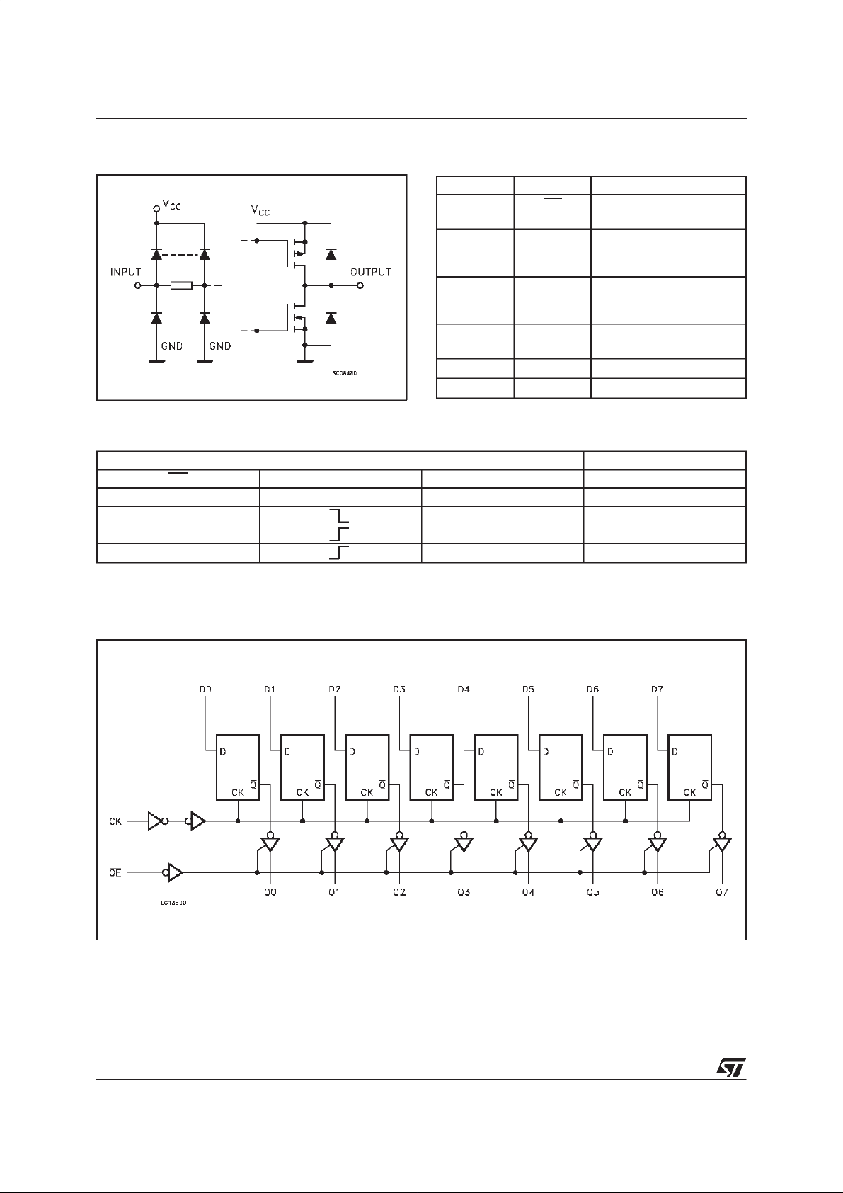
These 8 bit D-Type flip-flops are controlled by a
clockinput (CK)and an output enable input (OE).
On the positive transition of the clock, the Q
outputs will be set to logic state that were setup
at the D inputs.
2
MOStechnology.
74ACT574
OCTAL D-TYPE FLIP FLOP
DIP
ORDER CODES
PACKAGE TUBE T & R
DIP M74ACT574B
SOP M74ACT574M M74ACT574MTR
TSSOP M74ACT574TTR
While the (OE) input is low, the 8 outputs will be
in a normal logic state (high or low logic level)
and while high level the outputs will be in a high
impedancestate.
The output control does not affect the internal
operation of flip flop; that is, the old data can be
retained or the new data can be entered even
whilethe outputsare off.
The device is designed to interface directly High
Speed CMOS system with TTL and NMOS
components.
All inputs and outputs are equipped with
protection circuits against static discharge, giving
them 2KV ESD immunity and transient excess
voltage.
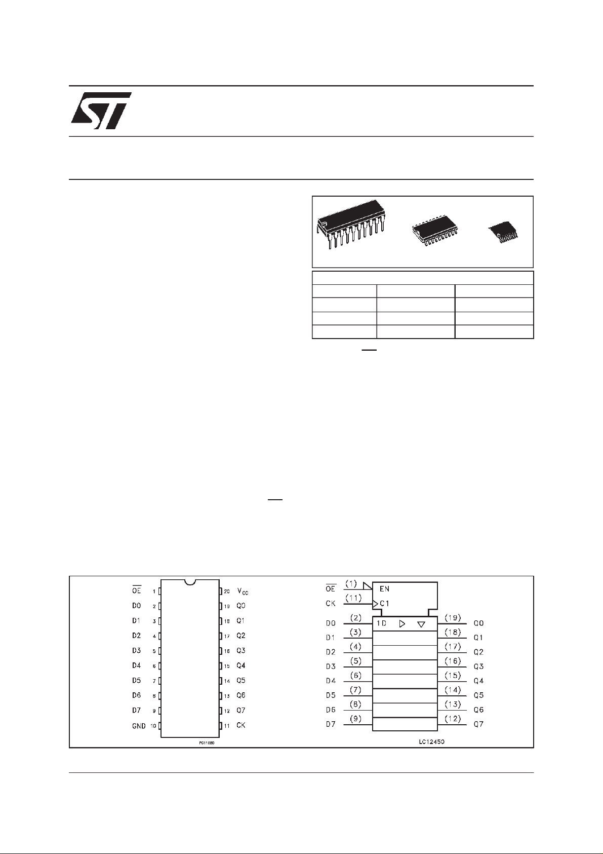
SOP
TSSOP
PIN CONNECTION AND IEC LOGICSYMBOLS
February 2000
1/11
Page 2
74ACT574
INPUT AND OUTPUT EQUIVALENTCIRCUIT PIN DESCRIPTION
PI N No SYMB OL NAME AND FUNCTIO N
1 OE 3 State Output Enable
2, 3, 4,
5, 6, 7,
8, 9
12, 13, 14,
15, 16, 17,
18, 19
11 CLOCK Clock Input (LOW to
10 GND Ground (0V)
20 V
TRUTH TABLE
INPUTS OUTPUTS
OE C K D Q
HXXZ
L X NO CHANGE
LLL
LHH
X:DON’TCARE
Z:HIGHIMPEDANCE
D0 to D7 Data Inputs
Q0 to Q7 3 State Outputs
CC
Input (Active LOW)
HIGH, edge triggered)
Positive Supply Voltage
LOGICDIAGRAMS
2/11
Page 3
74ACT574
ABSOLUTE MAXIMUM RATINGS
Symb o l Para met er Val u e Uni t
V
V
V
I
I
OK
I
or I
I
CC
T
T
AbsoluteMaximumRatingsarethosevalues beyond whichdamagetothedevicemayoccur. Functionaloperationunderthesecondition isnotimplied.
RECOMMENDEDOPERATINGCONDITIONS
Symb o l Parameter Val u e Uni t
V
V
V
T
dt/dv Input Rise and Fall Time V
1)VINfrom0.8Vto2.0V
Supply Voltage -0.5 to +7 V
CC
DC Input Voltage -0.5 to VCC+ 0.5 V
I
DC Output Voltage -0.5 to VCC+ 0.5 V
O
DC Input Diode Current ± 20 mA
IK
DC Output Diode Current ± 20 mA
DC Output Current
O
DC VCCor Ground Current
GND
Storage Temperature -65 to +150
stg
Lead Temperature (10 sec) 300
L
Supply Voltage 4.5 to 5.5 V
CC
Input Voltage 0 to V
I
Output Voltage 0 to V
O
Operating Temperature: -40 to +85
op
= 4.5 to 5.5V (note 1) 8 ns/V
CC
50 mA
±
400 mA
±
CC
CC
o
C
o
C
V
V
o
C
3/11
Page 4
74ACT574
DC SPECIFICATIONS
Symbol Parameter Test Conditions Value Unit
T
V
CC
(V)
High Level Input Voltage 4.5 VO= 0.1 V or
V
IH
5.5 2.0 1.5 2.0
Low Level Input Voltage 4.5 VO= 0.1 V or
V
IL
5.5 1.5 0.8 0.8
High Level Output
V
OH
Voltage
4.5
5.5 I
V
V
4.5 I
5.5 I
Low Level Output
V
OL
Voltage
4.5
5.5 I
V
V
4.5 I
5.5 I
Input Leakage Current 5.5 VI=VCCor GND ±0.1 ±1 µA
I
I
3 State Output Leakage
I
OZ
5.5 VI=VIHor V
Current
Max ICC/Input 5.5 VI=VCC-2.1V 0.6 1.5 mA
I
CCT
Quiescent Supply
I
CC
5.5 VI=VCCor GND 8 80 µA
-0.1 V
V
CC
V
-0.1 V
CC
IO=-50µA 4.4 4.49 4.4
(*)
=
I
IH
V
IL
(*)
I
IH
V
IL
=-50 µA 5.4 5.49 5.4
O
or
=-24 mA 3.86 3.76
O
=-24 mA 4.86 4.76
O
IO=50 µA 0.001 0.1 0.1
=
=50 mA 0.001 0.1 0.1
O
or
=24 mA 0.36 0.44
O
=24 mA 0.36 0.44
O
IL
VO=VCCor GND
Current
Dynamic Output Current
I
OLD
OHD
(note 1, 2)
I
1) Maximum test duration 2ms,one output loaded at time
2)Incidentwave switchingis guaranteedontransmissionlineswithimpedances aslowas50 Ω.
(*)All outputs loaded.
5.5 V
= 1.65 V max 75 mA
OLD
V
= 3.85 V min -75 mA
OHD
=25oC -40 to 85oC
A
Min. Typ. Max. Min. Max.
2.0 1.5 2.0
1.5 0.8 0.8
±0.5 ±5 µA
V
V
V
V
4/11
Page 5

74ACT574
AC ELECTRICAL CHARACTERISTICS
= 50 pF, RL= 500 Ω, Input tr=tf=3 ns)
(C
L
Symbol Parameter Test Condition Value Unit
t
Propagation Delay Time
PLH
t
CK to Q
PHL
Output Enable Time 5.0
t
PZL
t
PZH
t
Output Disable Time 5.0
PLH
t
PHL
t
CK Pulse Width, HIGH
w
V
(V)
5.0
5.0
CC
(*)
(*)
(*)
(*)
T
=25oC -40 to 85oC
A
Min. Typ. Max. Min. Max.
5.0 10.0 11.0 ns
5.5 9.0 10.0 ns
5.0 8.5 9.0 ns
1.5 3.0 4.0 ns
or LOW
Setup Time Q to CK
t
s
5.0
(*)
1.0 2.5 3.0 ns
HIGH or LOW
Hold Time Q to CK
t
h
5.0
(*)
-1.0 2.5 3.0 ns
HIGH or LOW
f
MAX
Maximim Clock
5.0
(*)
100 250 85 MHz
Frequency
(*) Voltagerangeis5V ± 0.5V
CAPACITIVE CHARACTERISTICS
Symbol Parameter Test Conditions Value Unit
T
V
CC
(V)
C
Output Capacitance 5.0 8 pF
OUT
Input Capacitance
C
IN
Power Dissipation
C
PD
5.0
5.0 26 pF
Capacitance (note 1)
1)CPDisdefinedasthevalue oftheIC’sinternal equivalentcapacitance whichiscalculated fromtheoperating current consumption withoutload.(Referto
TestCircuit).Averageoperatingcurrent canbeobtainedbythefollowingequation.I
(opr)= CPD• VCC• fIN+ICC/n(percircuit)
CC
=25oC -40 to 85oC
A
Min. Typ. Max. Min. Max.
4
pF
5/11
Page 6

74ACT574
TESTCIRCUIT
TEST SWITCH
t
PLH,tPHL
t
PZL,tPLZ
t
PZH,tPHZ
CL= 50 pF orequivalent (includes jig and probe capacitance)
=500Ωorequivalent
R
L=R1
R
ofpulse generator(typically50Ω)
T=ZOUT
Open
2V
CC
Open
WAVEFORM1: PROPAGATION DELAYS, SETUP AND HOLD TIMES (f=1MHz;50% duty cycle)
6/11
Page 7

74ACT574
WAVEFORM2: OUTPUTENABLEAND DISABLETIMES
(f=1MHz;50% duty cycle)
WAVEFORM3: PULSEWIDTH
7/11
Page 8

74ACT574
Plastic DIP-20 (0.25) MECHANICAL DATA
DIM.
MIN. TYP. MAX. MIN. TYP. MAX.
a1 0.254 0.010
B 1.39 1.65 0.055 0.065
b 0.45 0.018
b1 0.25 0.010
D 25.4 1.000
E 8.5 0.335
e 2.54 0.100
e3 22.86 0.900
F 7.1 0.280
I 3.93 0.155
L 3.3 0.130
Z 1.34 0.053
mm inch
8/11
P001J
Page 9

SO-20 MECHANICAL DATA
74ACT574
DIM.
MIN. TYP. MAX. MIN. TYP. MAX.
A 2.65 0.104
a1 0.10 0.20 0.004 0.007
a2 2.45 0.096
b 0.35 0.49 0.013 0.019
b1 0.23 0.32 0.009 0.012
C 0.50 0.020
c1 45 (typ.)
D 12.60 13.00 0.496 0.512
E 10.00 10.65 0.393 0.419
e 1.27 0.050
e3 11.43 0.450
F 7.40 7.60 0.291 0.299
L 0.50 1.27 0.19 0.050
M 0.75 0.029
S 8 (max.)
mm inch
P013L
9/11
Page 10

74ACT574
TSSOP20 MECHANICAL DATA
DIM.
mm inch
MIN. TYP. MAX. MIN. TYP. MAX.
A 1.1 0.433
A1 0.05 0.10 0.15 0.002 0.004 0.006
A2 0.85 0.9 0.95 0.335 0.354 0.374
b 0.19 0.30 0.0075 0.0118
c 0.09 0.2 0.0035 0.0079
D 6.4 6.5 6.6 0.252 0.256 0.260
E 6.25 6.4 6.5 0.246 0.252 0.256
E1 4.3 4.4 4.48 0.169 0.173 0.176
e 0.65 BSC 0.0256 BSC
K0
o
o
4
o
8
o
0
o
4
L 0.50 0.60 0.70 0.020 0.024 0.028
o
8
A
PIN 1 IDENTIFICATION
10/11
A2
A1
b
e
K
c
L
E
D
E1
1
Page 11

74ACT574
Information furnished isbelieved to be accurate and reliable. However, STMicroelectronics assumes no responsibility for the consequences
of use of such information nor for any infringement of patents or other rights of third parties which may result from its use. No license is
granted by implication or otherwise under any patent or patent rights of STMicroelectronics. Specification mentioned in this publication are
subject tochange without notice. Thispublication supersedes and replaces all information previously supplied. STMicroelectronics products
are not authorized for use as critical components in lifesupport devices or systems withoutexpress written approval of STMicroelectronics.
The ST logo is a registeredtrademark of STMicroelectronics
2000 STMicroelectronics – Printed in Italy – All RightsReserved
STMicroelectronics GROUP OF COMPANIES
Australia - Brazil - China - Finland - France - Germany - Hong Kong - India - Italy - Japan- Malaysia - Malta - Morocco
Singapore - Spain - Sweden - Switzerland - United Kingdom - U.S.A.
http://www.st.com
.
11/11
 Loading...