

Page 1
74ACT573
OCTAL D-TYPE LATCH
WITH 3 STATE OUTPUT NON INVERTING
■ HIGHSPEED:t
■
LOW POWER DISSIPATION:
I
=8 µA (MAX.) at TA=25oC
CC
■
COMPATIBLEWITHTTL OUTPUTS
V
=2V(MIN),VIL=0.8V(MAX)
IH
■ 50Ω TRANSMISSIONLINEDRIVING
=5ns(TYP.)atVCC=5V
PD
CAPABILITY
■ SYMMETRICALOUTPUTIMPEDANCE:
|I
|=IOL=24mA(MIN)
OH
■ BALANCEDPROPAGATIONDELAYS:
t
≅ t
PLH
PHL
■
OPERATINGVOLTAGERANGE:
V
(OPR)= 4.5Vto 5.5V
CC
■ PINANDFUNCTION COMPATIBLEWITH
74SERIES573
■ IMPROVEDLATCH-UP IMMUNITY
DESCRIPTION
The ACT573 is an advanced high-speed CMOS
OCTAL D-TYPE LATCH with 3 STATE OUTPUT
NON INVERTING fabricated with sub-micron
silicon gate and double-layermetal wiring C
2
MOS
technology. It is ideal for low power applications
mantaining high speed operation similar to
equivalentBipolarSchottky TTL.
These 8 bit D-Type latch are controlledby a latch
enable input (LE) and an output enable input
(OE).
M
(Micro Package)
B
(PlasticPackage)
ORDER CODES :
74ACT273B
74ACT273M
(TSSOPPackage)
T
While the LE inputs is held at a high level, the Q
outputs will follow the data input precisely or
inversely. When the LE is taken low, the Q
outputs will be latched precisely or inversely at
the logic level of D input data. While the (OE)
input is low, the 8 outputswill be in a normallogic
state (high or low logic level) and while high level
the outputs will be ina high impedancestate.
This device is designed to interface directly High
Speed CMOS systems with TTL and NMOS
components.
All inputs and outputs are equipped with
protection circuits against static discharge, giving
them 2KV ESD immunity and transient excess
voltage.
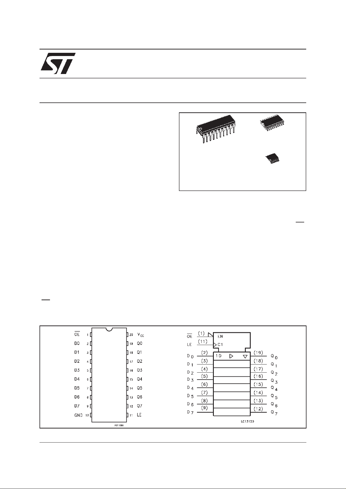
PIN CONNECTION AND IEC LOGIC SYMBOLS
May 1999
1/11
Page 2
74ACT573
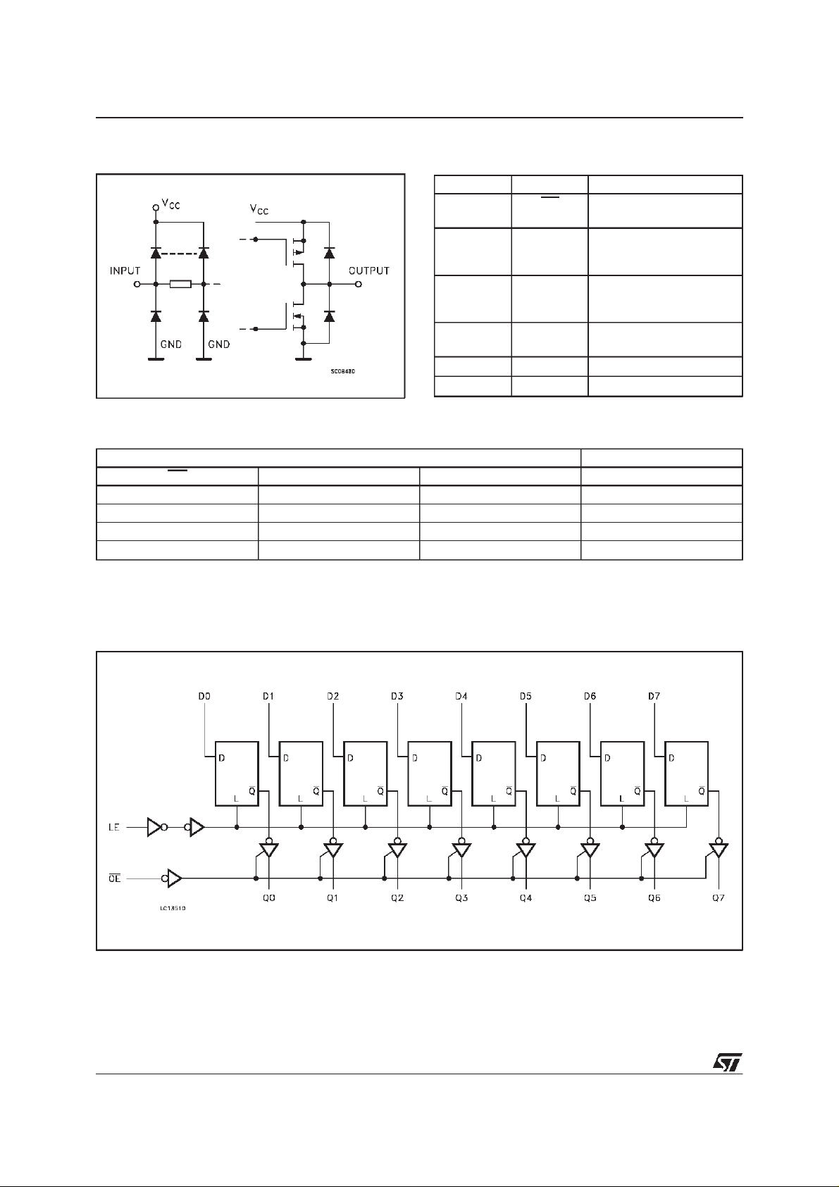
INPUT AND OUTPUT EQUIVALENTCIRCUIT PIN DESCRIPTION
PI N No SYMB OL NAME AND FUNCTIO N
1 OE 3 State Output Enable
2, 3, 4,
5, 6, 7,
8, 9
12, 13, 14,
15, 16, 17,
18, 19
11 LE Latch Enable
10 GND Ground (0V)
20 V
TRUTH TABLE
INPUTS OUTPUTS
OE CK D Q
HXXZ
L L X NO CHANGE *
LHLL
LHHH
X:DON’TCARE
Z:HIGHIMPEDANCE
*:Q OUTPUTSARELATCHEDATTHETIMEWHENTHELEINPUTISTAKENLOWLOGICLEVEL.
D0 to D7 Data Inputs
Q0 to Q7 3 State Outputs
CC
Input (Active LOW)
Input
Positive Supply Voltage
LOGICDIAGRAMS
2/11
Page 3
74ACT573
ABSOLUTE MAXIMUM RATINGS
Symb o l Paramet er Val u e Uni t
V
V
V
I
I
OK
I
or I
I
CC
T
T
AbsoluteMaximumRatingsarethosevaluesbeyondwhichdamagetothedevicemayoccur.Functionaloperation underthese conditionisnot implied.
RECOMMENDEDOPERATINGCONDITIONS
Symb o l Parameter Val u e Uni t
V
V
V
T
dt/dv Input Rise and Fall Time V
1)VINfrom0.8V to2.0V
Supply Voltage -0.5 to +7 V
CC
DC Input Voltage -0.5 to VCC+ 0.5 V
I
DC Output Voltage -0.5 to VCC+ 0.5 V
O
DC Input Diode Current ± 20 mA
IK
DC Output Diode Current ± 20 mA
DC Output Current
O
DC VCCor Ground Current
GND
Storage Temperature -65 to +150
stg
Lead Temperature (10 sec) 300
L
Supply Voltage 4.5 to 5.5 V
CC
Input Voltage 0 to V
I
Output Voltage 0 to V
O
Operating Temperature: -40 to +85
op
= 4.5 to 5.5V (note 1) 8 ns/V
CC
50 mA
±
400 mA
±
CC
CC
o
C
o
C
V
V
o
C
3/11
Page 4
74ACT573
DC SPECIFICATIONS
Symbol Parameter Test Conditi ons Value Unit
T
V
CC
(V)
High Level Input Voltage 4.5 VO= 0.1V or
V
IH
5.5 2.0 1.5 2.0
Low Level Input Voltage 4.5 VO= 0.1V or
V
IL
5.5 1.5 0.8 0.8
High Level Output
V
OH
Voltage
4.5
5.5 I
V
V
4.5 I
5.5 I
Low Level Output
V
OL
Voltage
4.5
5.5 I
V
V
4.5 I
5.5 I
Input Leakage Current 5.5 VI=VCCor GND ±0.1 ±1 µA
I
I
3 State Output Leakage
I
OZ
5.5 VI=VIHor V
Current
Max ICC/Input 5.5 VI=VCC-2.1V 0.6 1.5 mA
I
CCT
Quiescent Supply
I
CC
5.5 VI=VCCor GND 8 80 µA
-0.1 V
V
CC
V
-0.1 V
CC
IO=-50µA 4.4 4.49 4.4
(*)
=
I
IH
V
IL
(*)
I
IH
V
IL
=-50 µA 5.4 5.49 5.4
O
or
=-24 mA 3.86 3.76
O
=-24 mA 4.86 4.76
O
IO=50 µA 0.001 0.1 0.1
=
=50 mA 0.001 0.1 0.1
O
or
=24 mA 0.36 0.44
O
=24 mA 0.36 0.44
O
IL
VO=VCCor GND
Current
Dynamic Output Current
I
OLD
OHD
(note 1, 2)
I
1) Maximum test duration 2ms,one output loaded attime
2)Incident wave switchingis guaranteed ontransmissionlineswithimpedancesaslow as50 Ω.
(*)All outputs loaded.
5.5 V
= 1.65 V max 75 mA
OLD
V
= 3.85 V min -75 mA
OHD
=25oC -40 t o 85oC
A
Min. Typ. Max. Min. Max.
2.0 1.5 2.0
1.5 0.8 0.8
±0.5 ±5 µA
V
V
V
V
4/11
Page 5

74ACT573
AC ELECTRICAL CHARACTERISTICS
= 50 pF, RL= 500 Ω, Input tr=tf=3 ns)
(C
L
Symbol Parameter Test Con dition Value Unit
t
Propagation Delay Time
PLH
t
LE to Q
PHL
Propagation Delay Time
t
PLH
t
DtoQ
PHL
Output Enable Time 5.0
t
PZL
t
PZH
t
Output Disable Time 5.0
PLH
t
PHL
t
CK Pulse Width, HIGH
w
V
(V)
5.0
5.0
5.0
CC
(*)
(*)
(*)
(*)
(*)
T
=25oC -40 t o 85oC
A
Min. Typ. Max. Min. Max.
5.0 10.0 11.0 ns
5.0 10.0 11.0 ns
5.5 10.0 11.0 ns
6.5 11.0 12.0 ns
1.0 3.0 4.0 ns
or LOW
Setup Time Q to CK
t
s
5.0
(*)
0.0 2.0 3.0 ns
HIGH or LOW
Hold Time Q to CK
t
h
5.0
(*)
0.0 2.0 3.0 ns
HIGH or LOW
(*) Voltagerangeis5V ± 0.5V
CAPACITIVE CHARACTERISTICS
Symbol Parameter Test Conditi ons Value Unit
T
V
CC
(V)
C
Output Capacitance 5.0 8 pF
OUT
Input Capacitance
C
IN
Power Dissipation
C
PD
5.0
5.0 25 pF
Capacitance (note 1)
1)CPDisdefinedasthevalue oftheIC’sinternal equivalent capacitance whichis calculated fromtheoperating currentconsumption withoutload.(Referto
TestCircuit).Averageoperatingcurrentcanbeobtained bythefollowingequation.I
(opr)= CPD• VCC• fIN+ICC/n(percircuit)
CC
=25oC -40 t o 85oC
A
Min. Typ. Max. Min. Max.
4
pF
5/11
Page 6

74ACT573
TESTCIRCUIT
TEST SW ITCH
t
PLH,tPHL
t
PZL,tPLZ
t
PZH,tPHZ
CL= 50 pF or equivalent (includes jig and probe capacitance)
=500Ωorequivalent
R
L=R1
R
ofpulsegenerator (typically50Ω)
T=ZOUT
Open
2V
CC
Open
WAVEFORM1: LETO Qn PROPAGATIONDELAYS, LE MINIMUM PULSE WIDTH,
Dn TO LE SETUP AND HOLDTIMES (f=1MHz;50% duty cycle)
6/11
Page 7

74ACT573
WAVEFORM2: OUTPUTENABLE AND DISABLE TIMES
(f=1MHz;50% duty cycle)
WAVEFORM3: PROPAGATIONDELAY TIME (f=1MHz; 50% duty cycle)
7/11
Page 8

74ACT573
Plastic DIP-20 (0.25)MECHANICAL DATA
DIM.
MIN. TYP. MAX. MIN. TYP. MAX.
a1 0.254 0.010
B 1.39 1.65 0.055 0.065
b 0.45 0.018
b1 0.25 0.010
D 25.4 1.000
E 8.5 0.335
e 2.54 0.100
e3 22.86 0.900
F 7.1 0.280
I 3.93 0.155
L 3.3 0.130
Z 1.34 0.053
mm inch
8/11
P001J
Page 9

SO-20 MECHANICAL DATA
74ACT573
DIM.
MIN. TYP. MAX. MIN. TYP. MAX.
A 2.65 0.104
a1 0.10 0.20 0.004 0.007
a2 2.45 0.096
b 0.35 0.49 0.013 0.019
b1 0.23 0.32 0.009 0.012
C 0.50 0.020
c1 45 (typ.)
D 12.60 13.00 0.496 0.512
E 10.00 10.65 0.393 0.419
e 1.27 0.050
e3 11.43 0.450
F 7.40 7.60 0.291 0.299
L 0.50 1.27 0.19 0.050
M 0.75 0.029
S 8 (max.)
mm inch
P013L
9/11
Page 10

74ACT573
TSSOP20 MECHANICAL DATA
DIM.
mm inch
MIN. TYP. MAX. MIN. TYP. MAX.
A 1.1 0.433
A1 0.05 0.10 0.15 0.002 0.004 0.006
A2 0.85 0.9 0.95 0.335 0.354 0.374
b 0.19 0.30 0.0075 0.0118
c 0.09 0.2 0.0035 0.0079
D 6.4 6.5 6.6 0.252 0.256 0.260
E 6.25 6.4 6.5 0.246 0.252 0.256
E1 4.3 4.4 4.48 0.169 0.173 0.176
e 0.65 BSC 0.0256 BSC
K0
o
o
4
o
8
o
0
o
4
L 0.50 0.60 0.70 0.020 0.024 0.028
o
8
A
PIN 1 IDENTIFICATION
10/11
A2
A1
b
e
K
c
L
E
D
E1
1
Page 11

74ACT573
Information furnished is believed to be accurate and reliable. However, STMicroelectronics assumes no responsibility for the consequences
of use of such information nor for any infringement of patents or other rights of third parties which may result from its use. No license is
granted by implication or otherwise under any patent or patent rights of STMicroelectronics. Specification mentioned in thispublication are
subject tochange without notice. Thispublication supersedes and replaces all information previously supplied. STMicroelectronics products
are not authorized foruse as critical components inlife support devices or systems without express written approval of STMicroelectronics.
The ST logo is a trademark of STMicroelectronics
1999 STMicroelectronics – Printed in Italy – All Rights Reserved
STMicroelectronics GROUP OF COMPANIES
Australia - Brazil - Canada - China -France - Germany - Italy - Japan - Korea - Malaysia - Malta - Mexico - Morocco - The Netherlands -
Singapore - Spain -Sweden - Switzerland - Taiwan - Thailand - United Kingdom - U.S.A.
http://www.st.com
.
11/11
 Loading...