

Page 1
74ACT541
OCTAL BUS BUFFER
WITH 3 STATE OUTPUTS (NON INVERTED)
■ HIGH SPEED:t
■
LOW POWERDISSIPATION:
I
=8 µA(MAX.) at TA=25oC
CC
■
COMPATIBLEWITHTTLOUTPUTS
V
=2V(MIN),VIL=0.8V(MAX)
IH
■ 50Ω TRANSMISSIONLINEDRIVING
=4ns(TYP.)atVCC=5V
PD
CAPABILITY
■ SYMMETRICAL OUTPUTIMPEDANCE:
|I
|=IOL=24 mA(MIN)
OH
■ BALANCEDPROPAGATIONDELAYS:
t
≅ t
PLH
PHL
■
OPERATINGVOLTAGERANGE:
V
(OPR)= 4.5Vto 5.5V
CC
■ PINANDFUNCTION COMPATIBLEWITH
74SERIES541
■ IMPROVEDLATCH-UP IMMUNITY
DESCRIPTION
The ACT541 is an advanced CMOS OCTAL BUS
BUFFER (3-STATE) fabricated with sub-micron
silicon gate and double-layermetal wiring C
2
MOS
technology.It is ideal for low power applications
mantaining high speed operation similar to
eqivalentBipolar SchottkyTTL.
The 3 STATE control gate operates as a two
B
(PlasticPackage)
(Micro Package)
M
ORDERCODES :
74ACT541B 74ACT541M
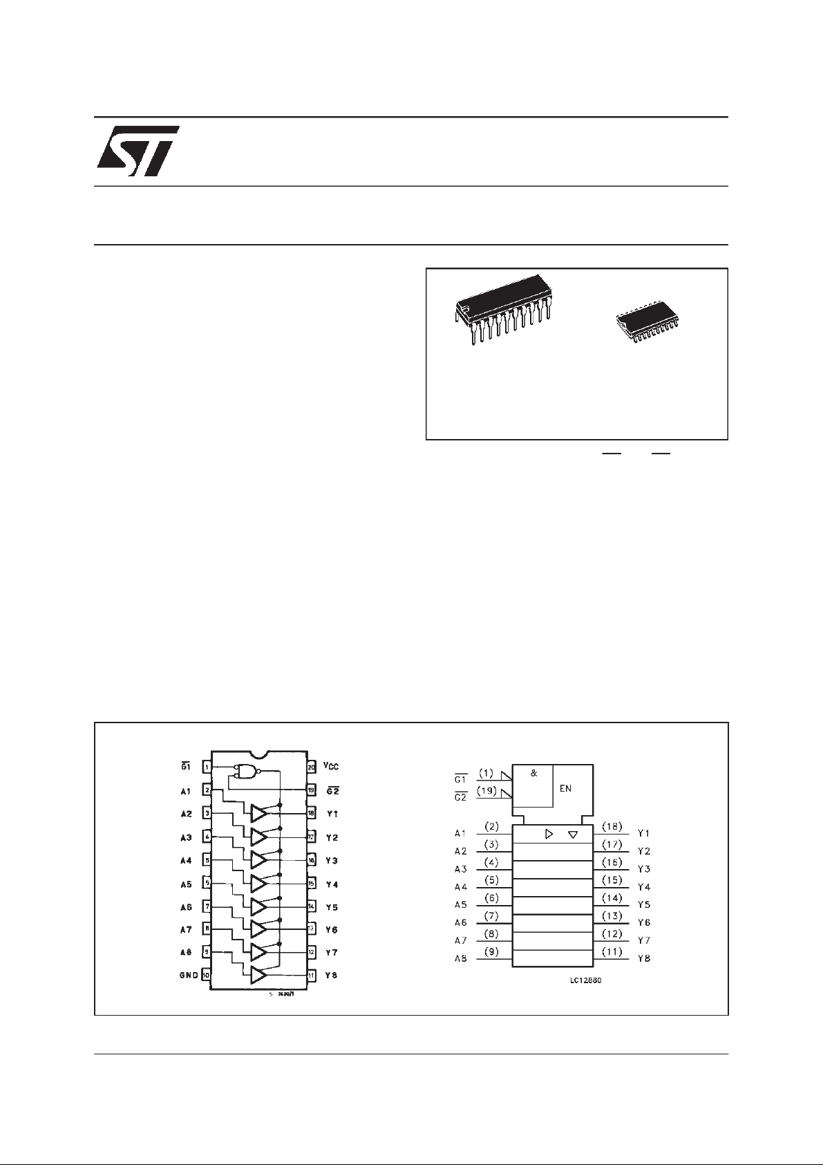
input AND such that if eitherG1 and G2 are high,
all eight outputs are in the high impedance state.
In order to enhance PC board layout, the AC541
offers a pinout having inputs and outputs on
opposite sidesof the package.
The device is designed to interface directly High
Speed CMOS systems with TTL, NMOS and
CMOSoutput voltage levels.
All inputs and outputs are equipped with
protection circuits against static discharge, giving
them 2KV ESD immunity and transient excess
voltage.
PIN CONNECTION AND IEC LOGIC SYMBOLS
December 1998
1/8
Page 2
74ACT541
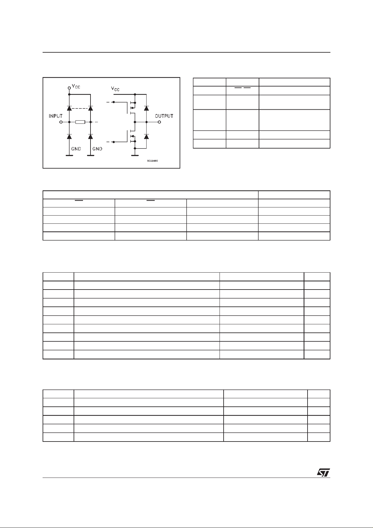
INPUT AND OUTPUT EQUIVALENT CIRCUIT
TRUTH TABLE
INPUT OUTPUT
G1 G2 An Yn
HXXZ
XHXZ
LLHH
LLLL
X:”H” or”L”
Z:Highimpedance
PIN DESCRIPTION
PI N No SYM BO L NAM E AND F U NCTIO N
1,19 G1,G2 Output Enable Input
2,3,4,5,
6,7,8,9
18,17,16,
15,14,13,
12, 11
10 GND Ground (0V)
20 V
A1toA8 Data Inputs
Y1toY8 Data Outputs
Positive Supply Voltage
CC
ABSOLUTE MAXIMUM RATINGS
Symb o l P ara met er Val u e Uni t
V
V
V
I
I
OK
I
orI
I
CC
T
T
AbsoluteMaximumRatingsarethosevalues beyondwhichdamagetothedevicemayoccur.Functionaloperationunderthese condition isnotimplied.
Supply Voltage -0.5to+7 V
CC
DC Input Voltage -0.5toVCC+0.5 V
I
DC Output Voltage -0.5toVCC+0.5 V
O
DC Input Diode Current
IK
DC Output Diode Current
DC Output Current ±50 mA
O
DC VCCor Ground Current ±400 mA
GND
Storage Temperature -65to+150
stg
Lead Temperature (10 sec) 300
L
20 mA
±
20 mA
±
o
C
o
C
RECOMMENDED OPERATINGCONDITIONS
Symb o l Parameter Val u e Uni t
V
V
V
T
dt/dv Input Rise and Fall Time V
1)VINfrom0.8V to2.0V
Supply Voltage 4.5to5.5 V
CC
Input Voltage 0toV
I
Output Voltage 0toV
O
Operating Temperature: -40to+85
op
= 4.5 to 5.5V (note 1) 8 ns/V
CC
CC
CC
V
V
o
C
2/8
Page 3
74ACT541
DC SPECIFICATIONS
Symbol Parameter Test Conditions Value Unit
T
V
CC
(V)
High Level Input Voltage 4.5 VO=0.1Vor
V
IH
5.5 2.0 1.5 2.0
Low Level Input Voltage 4.5 VO=0.1Vor
V
IL
5.5 1.5 0.8 0.8
High Level Output
V
OH
Voltage
4.5
5.5 I
V
V
4.5 I
5.5 I
Low Level Output
V
OL
Voltage
4.5
5.5 I
V
V
4.5 I
5.5 I
Input Leakage Current 5.5 VI=VCCorGND ±0.1 ±1 µA
I
I
3 State Output Leakage
I
OZ
5.5 VI=VIHorV
Current
Max ICC/Input 5.5 VI=VCC-2.1V 0.6 1.5 mA
I
CCT
Quiescent Supply
I
CC
5.5 VI=VCCorGND 4 40 µA
-0.1 V
V
CC
V
-0.1 V
CC
IO=-50µA 4.4 4.49 4.4
(*)
=
I
or
IH
V
IL
(*)
I
or
IH
V
IL
=-50µA 5.4 5.49 5.4
O
=-24 mA 3.86 3.76
O
=-24 mA 4.86 4.76
O
IO=50µA 0.001 0.1 0.1
=
=50mA 0.001 0.1 0.1
O
=24mA 0.36 0.44
O
=24mA 0.36 0.44
O
IL
VO=VCCorGND
Current
Dynamic Output Current
I
OLD
(note 1, 2)
I
OHD
1) Maximum testduration 2ms,one output loaded attime
2)Incident waveswitchingis guaranteed ontransmission lines withimpedances aslow as50 Ω.
5.5 V
=1.65V max 75 mA
OLD
V
=3.85V min -75 mA
OHD
=25oC -40 to 85oC
A
Min. Typ. Max. Min. Max.
2.0 1.5 2.0
1.5 0.8 0.8
±0.5 ±5 µA
V
V
V
V
AC ELECTRICAL CHARACTERISTICS
= 50 pF, RL= 500Ω, Input tr=tf=3 ns)
(C
L
Symbol Parameter Test Condition Value Unit
T
=25oC -40 to 85oC
A
Min. Typ. Max. Min. Max.
1.556.51.57.15
1.567.81.58.5
1.567.81.58.5
ns
ns
ns
t
Propagation Delay Time 5.0
PLH
t
PHL
t
Output Enable Time 5.0
PZL
t
PZH
t
Output Disable Time 5.0
PLZ
t
PHZ
(*) Voltagerangeis5V ± 0.5V
V
(V)
CC
(*)
(*)
(*)
CAPACITIVECHARACTERISTICS
Symb ol Pa rameter Tes t Con d i tions Valu e Unit
T
V
CC
(V)
Input Capacitance
C
IN
Power Dissipation
C
PD
5.0
5.0 22 pF
Capacitance (note 1)
1)CPDisdefined asthevalueof theIC’sinternalequivalentcapacitance whichis calculatedfromtheoperatingcurrentconsumption withoutload.(Referto
TestCircuit).Averageoperating current canbeobtained bythefollowingequation. I
(opr)= C
CC
=25oC -40 to 85oC
A
Min. Typ. Max. Min. Max.
4
•
•
f
IN+ICC
/8(per circuit)
V
PD
CC
pF
3/8
Page 4

74ACT541
TESTCIRCUIT
TEST SWITCH
t
PLH,tPHL
t
PZL,tPLZ
t
PZH,tPHZ
CL= 50 pFor equivalent (includes jigand probe capacitance)
=500Ωorequivalent
R
L=R1
R
ofpulsegenerator(typically50Ω)
T=ZOUT
Open
2V
CC
Open
WAVEFORM 1: PROPAGATIONDELAYS (f=1MHz; 50% duty cycle)
4/8
Page 5

74ACT541
WAVEFORM 2: OUTPUT ENABLEAND DISABLE TIME
(f=1MHz; 50% duty cycle)
5/8
Page 6

74ACT541
Plastic DIP-20 (0.25)MECHANICAL DATA
DIM.
MIN. TYP. MAX. MIN. TYP. MAX.
a1 0.254 0.010
B 1.39 1.65 0.055 0.065
b 0.45 0.018
b1 0.25 0.010
D 25.4 1.000
E 8.5 0.335
e 2.54 0.100
e3 22.86 0.900
F 7.1 0.280
I 3.93 0.155
L 3.3 0.130
Z 1.34 0.053
mm inch
6/8
P001J
Page 7

SO-20 MECHANICAL DATA
74ACT541
DIM.
MIN. TYP. MAX. MIN. TYP. MAX.
A 2.65 0.104
a1 0.10 0.20 0.004 0.007
a2 2.45 0.096
b 0.35 0.49 0.013 0.019
b1 0.23 0.32 0.009 0.012
C 0.50 0.020
c1 45 (typ.)
D 12.60 13.00 0.496 0.512
E 10.00 10.65 0.393 0.419
e 1.27 0.050
e3 11.43 0.450
F 7.40 7.60 0.291 0.299
L 0.50 1.27 0.19 0.050
M 0.75 0.029
S 8 (max.)
mm inch
P013L
7/8
Page 8

74ACT541
Information furnished is believed to be accurate and reliable. However, STMicroelectronics assumes no responsibility for the consequences
of use of such information nor for any infringement of patents or other rights of third parties which may result from its use. No license is
granted by implication or otherwise under any patent or patent rights of STMicroelectronics. Specification mentioned in this publication are
subject to change without notice. This publication supersedes and replaces all information previously supplied. STMicroelectronics products
are not authorized for use as critical components inlife support devices or systems without express written approval of STMicroelectronics.
The ST logo is a registered trademark of STMicroelectronics
1998 STMicroelectronics – Printed in Italy – All Rights Reserved
STMicroelectronics GROUP OF COMPANIES
Australia - Brazil - Canada -China - France - Germany - Italy - Japan - Korea - Malaysia - Malta - Mexico - Morocco - The Netherlands -
Singapore - Spain - Sweden - Switzerland - Taiwan - Thailand - United Kingdom - U.S.A.
http://www.st.com
.
8/8
 Loading...