

Datasheet 74ACT533SCX, 74ACT533SC, 74ACT533PC, 74ACT533MTCX, 74ACT533MTC Datasheet (Fairchild Semiconductor)
Page 1
© 1999 Fairchild Semiconductor Corporation DS500311 www.fairchildsemi.com
August 1999
Revised October 1999
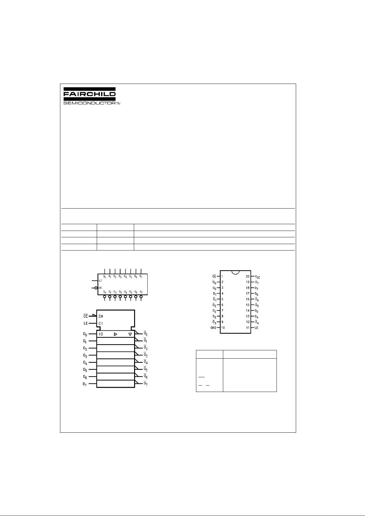
74ACT533 Octal Transparent Latch with 3-STATE Outputs
74ACT533
Octal Transparent Latch
with 3-STATE Outputs
General Description
The ACT533 consists of eigh t latches with 3-STATE outputs for bus organized system applications. The flip-f lops
appear transparent to the data whe n Latch En able (LE) is
HIGH. When LE is low, the data satisfying the input timi ng
requirements is latched. Data appears on the bus when the
Output Enable (OE) is LOW. When OE is HIGH, the bus
output is in the high impedance state.
Features
■ ICC and IOZ reduced by 50%
■ Eight latches in a single package
■ 3-STATE outputs drive bus lines or buffer memory
address registers
■ Outputs source/sink 24 mA
■ Inverted version of the ACT373
■ TTL-compatible inputs
Ordering Code:
Device also available in Tape and Reel. Specify by appending s uffix let te r “X” to the ordering code
Logic Symbols
IEEE/IEC
Connection Diagram
Pin Descriptions
FACT is a trade m ark of F airchild Semicondu ctor Corporation.
Order Number Package Number Package Description
74ACT533SC M20B 20-Lead Small Outline Integrated Circuit (SOIC), JEDEC MS-013, 0.300” Wide Body
74ACT533MTC MTC20 20-Lead Thin Shrink Small Outline Package (TSSOP), JEDEC MO-153, 4.4mm Wide
74ACT533PC N20A 20-Lead Plastic Dual-In-Line Package (PDIP), JEDEC MS-001, 0.300” Wide
Pin Names Description
D
0–D7
Data Inputs
LE Latch Enable Input
OE
Output Enable Input
O
0–O7
3-STATE Latch Outputs
Page 2
www.fairchildsemi.com 2
74ACT533
Functional Description
The ACT533 contain s eight D-type latches with 3 -STATE
standard outputs. When the Latch Enable (LE) input is
HIGH, data on the D
n
inputs enters the latches. In this con-
dition the latches are transparent, i.e., a latch o utput will
change state each time its D input cha nges. When LE is
LOW, the latches store the information that was present on
the D inputs at setup time preceding the HIGH-to-LOW
transition of LE. The 3-S TATE standard outputs are controlled by the Output E n able (OE
) input. When OE is LOW,
the standard outpu ts are in the 2 -state mode. W hen OE
is
HIGH, the standard outputs are in the high impedance
mode but this does not interfere with entering new data into
the latches.
Tr uth Table
H = HIGH Voltage Level
L = LOW Voltage Level
Z = High Impedance
X = Immaterial
O
0
= Previous O0 before HIGH-to-LOW transition of Latch Enable
Logic Diagram
Please note that this diagram is provided o nly f or t he understanding of lo gic operations and should not be used to estimate propagation delays.
Inputs Outputs
LE OE
D
n
O
n
X H X Z
H L L H
H L H L
L L X O
0
Page 3
3 www.fairchildsemi.com
74ACT533
Absolute Maximum Ratings(Note 1) Recommended Operating
Conditions
Note 1: Absolute maximum ratings are those values beyond which damage
to the device may occur. The databook specifications should be met, without exception, to ensure that the system design is reliable over its power
supply, temperature, and ou tput/inp ut load ing vari ables. Fairchild does n ot
recommend operat ion of FACT circuits outside da t abook specifications.
DC Electrical Characteristics
Note 2: All outputs loaded; thresholds on input associated with out put under test.
Note 3: Maximum test duration 2.0 ms, one output loaded at a time.
Supply Voltage (VCC) − 0.5V to + 7.0V
DC Input Diode Current (I
IK
)
V
I
= − 0.5V − 20 mA
V
I
= VCC + 0.5V + 20 mA
DC Input Voltage (V
I
) −0.5V to VCC + 0.5V
DC Output Diode Current (I
OK
)
V
O
= − 0.5V − 20 mA
V
O
= VCC + 0.5V + 20 mA
DC Output Voltage (V
O
) − 0.5V to VCC + 0.5V
DC Output Source
or Sink Current (I
O
) ± 50 mA
DC V
CC
or Ground Current
per Output Pin (I
CC
or I
GND
) ± 50 mA
Storage Temperature (T
STG
) − 65°C to + 150°C
DC Latchup Source
or Sink Current ± 300 mA
Junction Temperature (T
J
)
PDIP 140°C
Supply Voltage (V
CC
) 4.5V to 5.5V
Input Voltage (V
I
) 0V to V
CC
Output Voltage (VO) 0V to V
CC
Operating Temperature (TA) −40°C to +85°C
Minimum Input Edge Rate ∆V/∆t
V
IN
from 0.8V to 2.0V
V
CC
@ 4.5V, 5.5V 125 mV/ns
Symbol Parameter
V
CC
TA = +25°C TA = −40°C to +85°C
Units Conditions
(V) Typ Guaranteed Limits
V
IH
Minimum HIGH Level 4.5 1.5 2.0 2.0
V
V
OUT
= 0.1V
Input Voltage 5.5 1.5 2.0 2.0 or VCC − 0.1V
V
IL
Maximum LOW Level 4.5 1.5 0.8 0.8
V
V
OUT
= 0.1V
Input Voltage 5.5 1.5 0.8 0.8 or VCC − 0.1V
V
OH
Minimum HIGH Level 4.5 4.49 4.4 4.4
V I
OUT
= −50 µA
Output Voltage 5.5 5.49 5.4 5.4
VIN = V
IL
or V
IH
4.5 3.86 3.76 V IOH = −24 mA
5.5 4.86 4.76 IOH = −24 mA (Note 2)
V
OL
Maximum LOW Level 4.5 0.001 0.1 0.1
V I
OUT
= 50 µA
Output Voltage 5.5 0.001 0.1 0.1
VIN = V
IL
or V
IH
4.5 0.36 0.44 V IOL = 24 mA
5.5 0.36 0.44 IOL = 24 mA (Note 2)
I
IN
Maximum Input
5.5 ±0.1 ±1.0 µA VI = VCC, GND
Leakage Current
I
OZ
Maximum 3-STATE
5.5 ±0.25 ±2.5 µA
VI = VIL, V
IH
Leakage Current VO = VCC, GND
I
CCT
Maximum
5.5 0.6 1.5 mA VI = VCC − 2.1V
ICC/Input
I
OLD
Minimum Dynamic 5.5 75 mA V
OLD
= 1.65V Max
I
OHD
Output Current (Note 3) 5.5 −75 mA V
OHD
= 3.85V Min
I
CC
Maximum Quiescent
5.5 4.0 40.0 µA
VIN = V
CC
Supply Current or GND
Page 4

www.fairchildsemi.com 4
74ACT533
AC Electrical Characteristics
Note 4: Voltage Range 5.0 is 5. 0V ± 0.5V.
AC Operating Requirements
Note 5: Voltage Range 5.0 is 5. 0V ± 0.5V.
Capacitance
Symbol Parameter
V
CC
TA = + 25°CT
A
= − 40°C to + 85°C
Units
(V)
C
L
= 50 pF CL = 50 pF
(Note 4) Min Typ Max Min Max
t
PHL
Propagation Delay
5.0 2.0 6.0 8.0 2.0 8.5 ns
t
PLH
Dn to O
n
t
PHL
Propagation Delay
5.0 2.5 7.0 9.0 2.5 9.5 ns
t
PLH
LE to O
n
t
PZL
, t
PZH
Output Enable Time 5.0 2.0 7.0 9.0 2.0 9.5 ns
t
PHZ
, t
PLZ
Output Disable Time 5.0 1.0 8.0 10.0 1.0 10.5 ns
Symbol Par ameter
V
CC
TA = + 25°CT
A
= − 40°C to + 85°C
Units
(V)
C
L
= 50 pF CL = 50 pF
(Note 5) Typ Guaranteed Minimum
t
S
Setup Time, HIGH or LOW
5.0 0 3.0 3.0 ns
D
n
to LE
t
H
Hold Time, HIGH or LOW
5.0 0 1.5 1.5 ns
D
n
to LE
t
W
LE Pulse Width, HIGH 5.0 2.0 4.0 4.0 ns
Symbol Parameter Typ Units Conditions
C
IN
Input Capacitance 4.5 pF VCC = OPEN
C
PD
Power Dissipation Capacitance 40 pF VCC = 5.0V
Page 5

5 www.fairchildsemi.com
74ACT533
Physical Dimensions inches (millimeters) unless otherwise noted
20-Lead Small Outline Integrated Circuit, JEDEC MS-013, 0.300” Wide Body
Package Number M20B
Page 6

www.fairchildsemi.com 6
74ACT533
Physical Dimensions inches (millimeters) unless otherwise noted (Continued)
20-Lead Thin Shrink Small Outline Package (TSSOP), JEDEC MO-153, 4.4mm Wide
Package Number MTC20
Page 7

Physical Dimensions inches (millimeters) unless otherwise noted (Continued)
7 www.fairchildsemi.com
74ACT533 Octal Transparent Latch with 3-STATE Outputs
Physical Dimensions inches (millimeters) unless otherwise noted (Continued)
20-Lead Plastic Dual-In-Line Package, JEDEC MS-001, 0.300” Wide
Package Number N20A
Fairchild does not assume any responsibility for use of any circu itry described, no circuit patent license s are implied and
Fairchild reserves the right at any time without notice to change said circuitry and specifications.
LIFE SUPPORT POLICY
FAIRCHILD’S PRODUCTS ARE NOT AUTHORIZED FOR USE AS CRITICAL COMPONENTS IN LIFE SUPPORT
DEVICES OR SYSTEMS WITHOUT THE EXPRESS WRITTEN APPROVAL OF THE PRESIDENT OF FAIRCHILD
SEMICONDUCTOR CORPORATION. As used herein:
1. Life support devices or systems are dev ic es or syste ms
which, (a) are intended for surgical implant into the
body, or (b) support or sustain life, and (c) whose failure
to perform when properly used in accordance with
instructions for use provided i n the labe li ng, can be re asonably expected to result in a significant injury to the
user.
2. A critical componen t in any com ponent o f a l ife supp ort
device or system whose failu re to perform can b e reasonably expected to c ause th e fa i lure of the li fe s upp or t
device or system, or to affect its safety or effectiveness.
www.fairchildsemi.com
 Loading...