

Page 1
74ACT245
OCTAL BUS TRANSCEIVER (3-STATE)
■ HIGHSPEED:t
■
LOW POWER DISSIPATION:
I
=8 µA (MAX.) at TA=25oC
CC
■
COMPATIBLEWITH TTLOUTPUTS
V
=2V(MIN)VIL=0.8V (MAX)
IH
■ 50ΩTRANSMISSIONLINEOUTPUT DRIVE
=5.5ns(TYP.)atVCC=5V
PD
CAPABILITY
■ SYMMETRICALOUTPUTIMPEDANCE:
|I
|=IOL=24mA(MIN)
OH
■ BALANCEDPROPAGATIONDELAYS:
t
≅ t
PLH
PHL
■
OPERATINGVOLTAGERANGE:
V
(OPR)= 4.5Vto 5.5V
CC
■ PINANDFUNCTION COMPATIBLEWITH
74SERIES245
■ IMPROVEDLATCH-UP IMMUNITY
DESCRIPTION
The ACT245 is an advanced CMOS OCTAL BUS
TRANSCEIVER (3-STATE) fabricated with
sub-micron silicon gate and double-layer metal
wiring C
2
MOS technology. It is ideal for low
power applications mantaining high speed
operation similar to equivalent Bipolar Schottky
TTL.
This IC is intended for two-way asynchronous
communication between data buses and the
M
(Micro Package)
B
(PlasticPackage)
ORDER CODES :
74ACT245B
74ACT245M
(TSSOPPackage)
T
74ACT245T
direction of data trasmission is determined by
DIR input. The enable input G can be used to
disable the device so that the buses are
effectivelyisolated.
All inputs and outputs are equipped with
protection circuits against static discharge, giving
them 2KV ESD immunity and transient excess
voltage.
IT IS PROHIBITED TO APPLY A SIGNAL TO A
TERMINAL WHEN IT IS IN OUTPUT MODE
AND WHEN A BUS THERMINAL IS FLOATING
(HIGH IMPEDANCE STATE) IT IS REQUESTED
TO FIX THE INPUT LEVEL BY MEANS OF
EXTERNAL PULL DOWN OR PULL UP
RESISTOR.
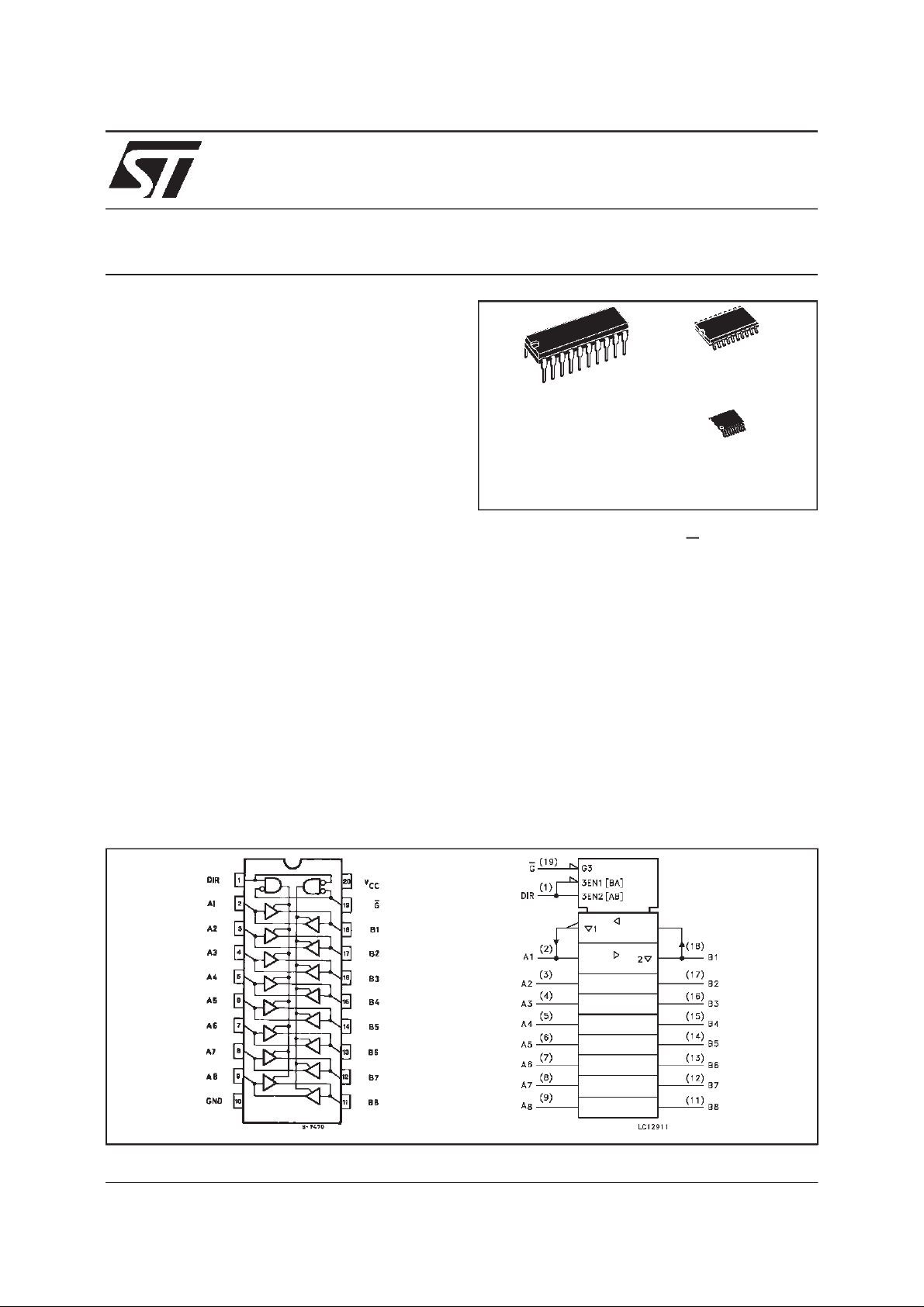
PIN CONNECTION AND IEC LOGICSYMBOLS
May 1999
1/9
Page 2
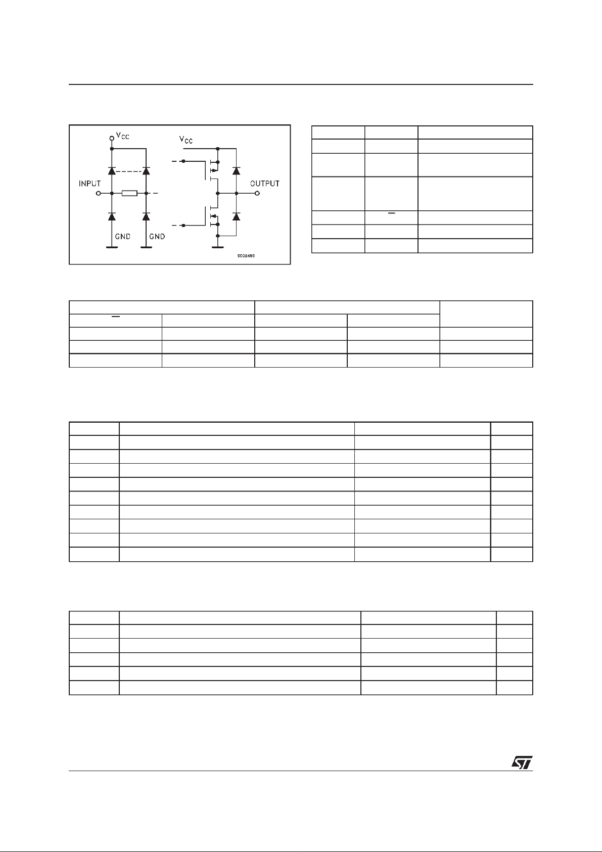
74ACT245
INPUT AND OUTPUT EQUIVALENTCIRCUIT
TRUTH TABLE
INP UT FUNCTIO N OUT P UT
GDIRABUSBBUS
LLOUTPUTINPUTA=B
LHINPUTOUTPUTB=A
HXZZZ
X:”H” or”L”
Z:Highimpedance
PIN DESCRIPTION
PI N No SYM BO L NAM E AN D F U NCTI O N
1 DIR Directional Control
2,3,4,5,
6,7,8,9
18,17, 16,
15,14, 13,
12, 11
19 G Output Enabel Input
10 GND Ground (0V)
20 V
A1toA8 Data Inputs/Outputs
B1toB8 Data Inputs/Outputs
Positive Supply Voltage
CC
ABSOLUTE MAXIMUM RATINGS
Symb o l Para met er Val u e Uni t
V
V
V
I
I
OK
I
orI
I
CC
T
T
AbsoluteMaximum Ratingsarethosevalues beyond whichdamageto thedevicemayoccur. Functionaloperationundertheseconditionisnotimplied.
Supply Voltage -0.5to+7 V
CC
DC Input Voltage -0.5toVCC+0.5 V
I
DC Output Voltage -0.5toVCC+0.5 V
O
DC Input Diode Current ±20 mA
IK
DC Output Diode Current ±20 mA
DC Output Current ±50 mA
O
DC VCCor Ground Current
GND
Storage Temperature -65to+150
stg
Lead Temperature (10 sec) 300
L
400 mA
±
o
C
o
C
RECOMMENDED OPERATINGCONDITIONS
Symb o l Parameter Val u e Uni t
V
V
V
T
dt/dv Input Rise and Fall Time V
1)VINfrom0.8V to2.0V
Supply Voltage 4.5to5.5 V
CC
Input Voltage 0toV
I
Output Voltage 0toV
O
Operating Temperature: -40to+85
op
= 4.5 to 5.5V (note 1) 8 ns/V
CC
CC
CC
V
V
o
C
2/9
Page 3

74ACT245
DC SPECIFICATIONS
Symbol Parameter Test Conditi ons Value Unit
T
V
CC
(V)
High Level Input Voltage 4.5 VO=0.1Vor
V
IH
5.5 2.0 1.5 2.0
Low Level Input Voltage 4.5 VO=0.1Vor
V
IL
5.5 1.5 0.8 0.8
High Level Output
V
OH
Voltage
4.5
5.5 I
V
V
4.5 I
5.5 I
Low Level Output
V
OL
Voltage
4.5
5.5 I
V
V
4.5 I
5.5 I
Input Leakage Current 5.5 VI=VCCorGND ±0.1 ±1 µA
I
I
3 State Output Leakage
I
OZ
5.5 VI=VIHorV
Current
Max ICC/Input 5.5 VI=VCC-2.1V 0.6 1.5 mA
I
CCT
Quiescent Supply
I
CC
5.5 VI=VCCorGND 8 80 µA
-0.1V
V
CC
V
-0.1V
CC
IO=-50µA 4.4 4.49 4.4
(*)
=
I
or
IH
V
IL
(*)
I
or
IH
V
IL
=-50µA 5.4 5.49 5.4
O
=-24 mA 3.86 3.76
O
=-24 mA 4.86 4.76
O
IO=50µA 0.001 0.1 0.1
=
=50µA 0.001 0.1 0.1
O
=24mA 0.36 0.44
O
=24mA 0.36 0.44
O
IL
VO=VCCorGND
Current
Dynamic Output Current
I
OLD
(note 1, 2)
I
OHD
1) Maximum test duration 2ms, one output loaded attime
2)Incident waveswitchingisguaranteed ontransmission lineswithimpedances aslowas50 Ω.
(*)All outputs loaded.
5.5 V
=1.65V max 75 mA
OLD
V
=3.85V min -75 mA
OHD
=25oC -40 to 85oC
A
Min. Typ. Max. Min. Max.
2.0 1.5 2.0
1.5 0.8 0.8
±0.5 ±5 µA
V
V
V
V
3/9
Page 4

74ACT245
AC ELECTRICAL CHARACTERISTICS
= 50 pF, RL= 500 Ω, Input tr=tf=3 ns)
(C
L
Symbol Parameter Test Conditio n Value Unit
t
Propagation Delay Time 5.0
PLH
t
PHL
t
Output Enable Time 5.0
PZL
t
PZH
t
Output Disable Time 5.0
PLZ
t
PHZ
(*) Voltagerangeis 5V± 0.5V
V
(V)
CC
(*)
(*)
(*)
T
=25oC -40 to 85oC
A
Min. Typ. Max. Min. Max.
1.5 5.5 8.0 1.5 9.0
1.5 6.5 10.0 1.5 12.0
1.5 7.5 10.0 1.5 11.0
ns
ns
ns
CAPACITIVE CHARACTERISTICS
Symbol Parameter Test Conditi ons Value Unit
T
V
CC
(V)
Input Capacitance
C
IN
I/O Capacitance
C
i/o
Power Dissipation
C
PD
5.0
5.0
5.0 23 pF
Capacitance (note 1)
1)CPDisdefinedas thevalueoftheIC’sinternal equivalent capacitance whichiscalculated fromtheoperatingcurrentconsumption without load.(Referto
TestCircuit).Average operatingcurrentcanbe obtainedbythefollowingequation.I
(opr)=CPD• VCC• fIN+ICC/n(percircuit)
CC
=25oC -40 to 85oC
A
Min. Typ. Max. Min. Max.
5
10
pF
pF
TESTCIRCUIT
TEST SWITCH
t
PLH,tPHL
t
PZL,tPLZ
t
PZH,tPHZ
CL= 50 pF or equivalent (includes jigand probe capacitance)
R
=500Ωorequivalent
L=R1
R
ofpulsegenerator (typically50Ω)
T=ZOUT
Open
2V
CC
Open
4/9
Page 5

74ACT245
WAVEFORM 1: PROPAGATIONDELAYS
(f=1MHz;50% duty cycle)
WAVEFORM 2: OUTPUT ENABLEAND DISABLE TIME (f=1MHz; 50% duty cycle)
5/9
Page 6

74ACT245
Plastic DIP-20 (0.25) MECHANICAL DATA
DIM.
MIN. TYP. MAX. MIN. TYP. MAX.
a1 0.254 0.010
B 1.39 1.65 0.055 0.065
b 0.45 0.018
b1 0.25 0.010
D 25.4 1.000
E 8.5 0.335
e 2.54 0.100
e3 22.86 0.900
F 7.1 0.280
I 3.93 0.155
L 3.3 0.130
Z 1.34 0.053
mm inch
6/9
P001J
Page 7

SO-20 MECHANICAL DATA
74ACT245
DIM.
MIN. TYP. MAX. MIN. TYP. MAX.
A 2.65 0.104
a1 0.10 0.20 0.004 0.007
a2 2.45 0.096
b 0.35 0.49 0.013 0.019
b1 0.23 0.32 0.009 0.012
C 0.50 0.020
c1 45 (typ.)
D 12.60 13.00 0.496 0.512
E 10.00 10.65 0.393 0.419
e 1.27 0.050
e3 11.43 0.450
F 7.40 7.60 0.291 0.299
L 0.50 1.27 0.19 0.050
M 0.75 0.029
S 8 (max.)
mm inch
P013L
7/9
Page 8

74ACT245
TSSOP20 MECHANICAL DATA
DIM.
mm inch
MIN. TYP. MAX. MIN. TYP. MAX.
A 1.1 0.433
A1 0.05 0.10 0.15 0.002 0.004 0.006
A2 0.85 0.9 0.95 0.335 0.354 0.374
b 0.19 0.30 0.0075 0.0118
c 0.09 0.2 0.0035 0.0079
D 6.4 6.5 6.6 0.252 0.256 0.260
E 6.25 6.4 6.5 0.246 0.252 0.256
E1 4.3 4.4 4.48 0.169 0.173 0.176
e 0.65 BSC 0.0256 BSC
K0
o
o
4
o
8
o
0
o
4
L 0.50 0.60 0.70 0.020 0.024 0.028
o
8
A
PIN 1 IDENTIFICATION
8/9
A2
A1
b
e
K
c
L
E
D
E1
1
Page 9

74ACT245
Information furnished is believed to be accurate and reliable. However, STMicroelectronics assumes no responsibility for the consequences
of use of such information nor for any infringement of patents or other rights of third parties which may result from its use. No license is
granted by implication or otherwise under any patent or patent rights of STMicroelectronics. Specification mentioned in this publication are
subject tochange without notice. This publication supersedes and replaces all information previously supplied. STMicroelectronics products
are not authorized for use as critical components inlife support devices or systems without express written approval of STMicroelectronics.
The ST logo is a trademark of STMicroelectronics
1999 STMicroelectronics – Printed in Italy – All Rights Reserved
STMicroelectronics GROUP OF COMPANIES
Australia - Brazil - Canada - China -France -Germany - Italy - Japan - Korea -Malaysia - Malta - Mexico - Morocco - The Netherlands -
Singapore - Spain -Sweden - Switzerland - Taiwan - Thailand - United Kingdom - U.S.A.
http://www.st.com
.
9/9
 Loading...