

Page 1
74ACT244
OCTAL BUS BUFFER
WITH 3 STATE OUTPUTS (NON INVERTED)
■ HIGH SPEED:t
■
LOW POWERDISSIPATION:
I
=8 µA(MAX.) at TA=25oC
CC
■
COMPATIBLEWITH TTL OUTPUTS
V
=2V(MIN),VIL=0.8V(MAX)
IH
■ 50Ω TRANSMISSIONLINEDRIVING
=4.5ns (TYP.)atVCC=5V
PD
CAPABILITY
■ SYMMETRICAL OUTPUTIMPEDANCE:
|I
|=IOL=24 mA(MIN)
OH
■ BALANCEDPROPAGATIONDELAYS:
t
≅ t
PLH
PHL
■
OPERATINGVOLTAGERAN GE:
V
(OPR)= 4.5Vto 5.5V
CC
■ PINANDFUNCTION COMPATIBLEWITH
74SERIES244
■ IMPROVEDLATCH-UPIMMUNITY
DESCRIPTION
The ACT244 is an advanced CMOS OCTAL BUS
BUFFER (3-STATE) fabricated with sub-micron
silicon gate and double-layermetal wiring C
2
MOS
technology. It is ideal for low power applications
mantaining high speed operation similar to
equivalentBipolar Schottky TTL.
M
(Micro Package)
B
(PlasticPackage)
ORDER CODES:
74ACT244B
74ACT244M
(TSSOPPackage)
T
74ACT244T
G control output governsfourBUS BUFFERs.
This device is desibned to be used with 3 state
memoryaddressdrivers, etc.
The device is designed to interface directly High
Speed CMOS systems with TTL, NMOS and
CMOSoutputvoltage levels.
All inputs and outputs are equipped with
protection circuits against static discharge, giving
them 2KV ESD immunity and transient excess
voltage.
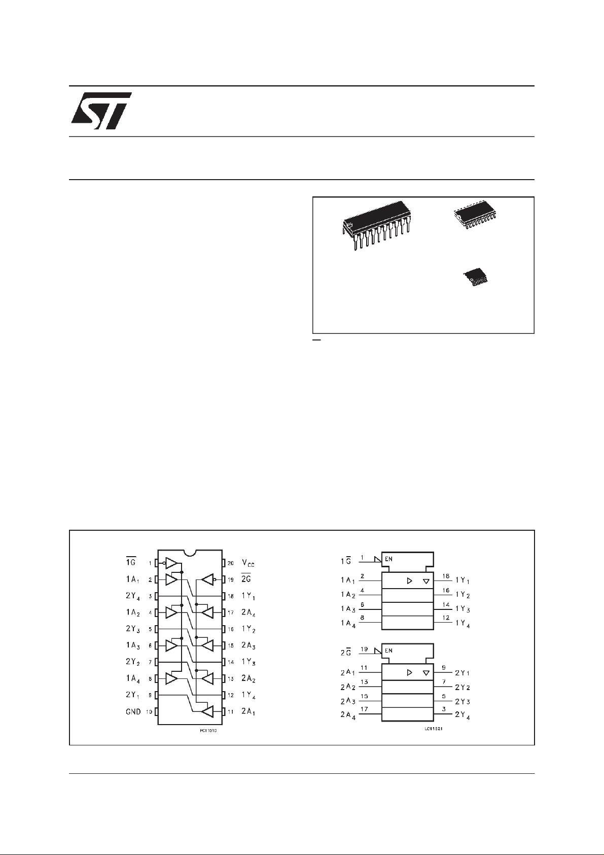
PIN CONNECTION AND IEC LOGIC SYMBOLS
February 1999
1/9
Page 2
74ACT244
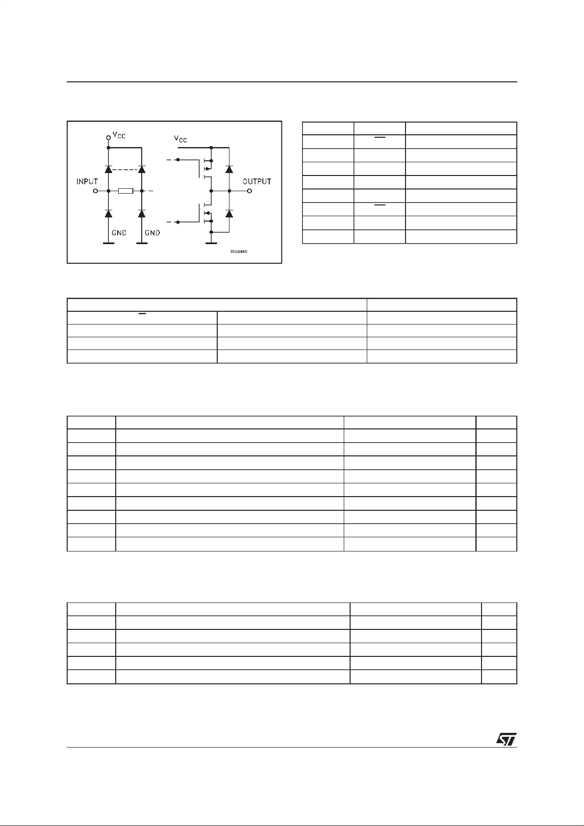
INPUT AND OUTPUT EQUIVALENTCIRCUIT
TRUTH TABLE
INPUT OUTPU T
GAnYn
LLL
LHH
HXZ
X:”H” or”L”
Z:Highimpedance
PIN DESCRIPTION
PI N No SYM BO L NAM E AN D FUNCTION
1 1G Output Enable Input
2,4,6,8 1A1to1A4 Data Inputs
9,7,5,3 2Y1to2Y4 Data Outputs
11,13,15,17 2A1to2A4 Data Inputs
18,16,14,12 1Y1to1Y4 Data Outputs
19 2G Output Enabel Input
10 GND Ground (0V)
20 V
Positive Supply Voltage
CC
ABSOLUTE MAXIMUM RATINGS
Symb o l Para met er Val u e Uni t
V
V
V
I
I
OK
I
orI
I
CC
T
T
AbsoluteMaximumRatingsarethosevaluesbeyond whichdamagetothedevice mayoccur. Functionaloperationunderthese condition isnotimplied.
Supply Voltage -0.5to+7 V
CC
DC Input Voltage -0.5toVCC+0.5 V
I
DC Output Voltage -0.5toVCC+0.5 V
O
DC Input Diode Current ±20 mA
IK
DC Output Diode Current ±20 mA
DC Output Current ±50 mA
O
DC VCCor Ground Current ±400 mA
GND
Storage Temperature -65to+150
stg
Lead Temperature (10 sec) 300
L
o
C
o
C
RECOMMENDED OPERATING CONDITIONS
Symb o l Parameter Val u e Uni t
V
V
V
T
dt/dv Input Rise and Fall Time V
1)VINfrom0.8V to2.0V
Supply Voltage 4.5to5.5 V
CC
Input Voltage 0toV
I
Output Voltage 0toV
O
Operating Temperature: -40to+85
op
= 4.5 to 5.5V (note 1) 8 ns/V
CC
CC
CC
V
V
o
C
2/9
Page 3
74ACT244
DC SPECIFICATIONS
Symbol Parameter Test Conditions Value Unit
T
V
CC
(V)
High Level Input Voltage 4.5 VO=0.1V or
V
IH
5.5 2.0 1.5 2.0
Low Level Input Voltage 4.5 VO=0.1V or
V
IL
5.5 1.5 0.8 0.8
High Level Output
V
OH
Voltage
4.5
5.5 I
V
V
4.5 I
5.5 I
Low Level Output
V
OL
Voltage
4.5
5.5 I
V
V
4.5 I
5.5 I
Input Leakage Current 5.5 VI=VCCorGND ±0.1 ±1 µA
I
I
3 State Output Leakage
I
OZ
5.5 VI=VIHorV
Current
Max ICC/Input 5.5 VI=VCC-2.1V 0.6 1.5 mA
I
CCT
Quiescent Supply
I
CC
5.5 VI=VCCorGND 8 80 µA
-0.1V
V
CC
V
-0.1V
CC
IO=-50µA 4.4 4.49 4.4
(*)
=
I
or
IH
V
IL
(*)
I
or
IH
V
IL
=-50µA 5.4 5.49 5.4
O
=-24 mA 3.86 3.76
O
=-24 mA 4.86 4.76
O
IO=50µA 0.001 0.1 0.1
=
=50mA 0.001 0.1 0.1
O
=24mA 0.36 0.44
O
=24mA 0.36 0.44
O
IL
VO=VCCorGND
Current
Dynamic Output Current
I
OLD
(note 1, 2)
I
OHD
1) Maximum test duration 2ms, one output loaded attime
2)Incidentwave switchingisguaranteed ontransmission lineswithimpedances aslowas 50 Ω.
(*)All outputs loaded.
5.5 V
=1.65V max 75 mA
OLD
V
=3.85V min -75 mA
OHD
=25oC -40 t o 85oC
A
Min. Typ. Max. Min. Max.
2.0 1.5 2.0
1.5 0.8 0.8
±0.5 ±5 µA
V
V
V
V
3/9
Page 4

74ACT244
AC ELECTRICAL CHARACTERISTICS (CL= 50 pF, RL= 500 Ω, Input tr=tf=3 ns)
Symbol Parameter Test Condition Value Unit
V
CC
(V)
t
Propagation Delay Time 5.0
PLH
t
PHL
Output Enable Time 5.0
t
PZL
t
PZH
t
Output Disable Time 5.0
PLZ
t
PHZ
(*)Voltagerange is5V ±0.5V
(*)
(*)
(*)
CAPACITIVE CHARACTERISTICS
Symbol Parameter Test Conditions Value Unit
V
CC
(V)
C
Input Capacitance
IN
I/O Capacitance
C
i/o
Power Dissipation
C
PD
Capacitance (note 1)
1)CPDisdefinedasthevalueoftheIC’sinternal equivalentcapacitance whichis calculated fromtheoperatingcurrentconsumption withoutload.(Referto
TestCircuit).Average operatingcurrent canbeobtained bythefollowingequation.I
5.0
5.0
5.0 24 pF
(opr)= CPD• VCC• fIN+ICC/n(percircuit)
CC
T
=25oC -40 t o 85oC
A
Min. Typ. Max. Min. Max.
1.5 4.5 9.0 1.5 10.0 ns
1.5 5.5 9.0 1.5 10.0 ns
1.5 6.5 10.0 1.5 11.0 ns
=25oC -40 t o 85oC
T
A
Min. Typ. Max. Min. Max.
4
8
pF
pF
TESTCIRCUIT
TEST SWITCH
t
PLH,tPHL
t
PZL,tPLZ
t
PZH,tPHZ
CL= 50 pF or equivalent (includes jig and probe capacitance)
=500Ω orequivalent
R
L=R1
R
ofpulsegenerator(typically50Ω)
T=ZOUT
Open
2V
CC
Open
4/9
Page 5

74ACT244
WAVEFORM 1: PROPAGATIONDELAYS
(f=1MHz;50% dutycycle)
WAVEFORM 2: OUTPUTENABLE AND DISABLE TIME(f=1MHz; 50% duty cycle)
5/9
Page 6

74ACT244
Plastic DIP-20 (0.25) MECHANICAL DATA
DIM.
MIN. TYP. MAX. MIN. TYP. MAX.
a1 0.254 0.010
B 1.39 1.65 0.055 0.065
b 0.45 0.018
b1 0.25 0.010
D 25.4 1.000
E 8.5 0.335
e 2.54 0.100
e3 22.86 0.900
F 7.1 0.280
I 3.93 0.155
L 3.3 0.130
Z 1.34 0.053
mm inch
6/9
P001J
Page 7

SO-20 MECHANICAL DATA
74ACT244
DIM.
MIN. TYP. MAX. MIN. TYP. MAX.
A 2.65 0.104
a1 0.10 0.20 0.004 0.007
a2 2.45 0.096
b 0.35 0.49 0.013 0.019
b1 0.23 0.32 0.009 0.012
C 0.50 0.020
c1 45 (typ.)
D 12.60 13.00 0.496 0.512
E 10.00 10.65 0.393 0.419
e 1.27 0.050
e3 11.43 0.450
F 7.40 7.60 0.291 0.299
L 0.50 1.27 0.19 0.050
M 0.75 0.029
S 8 (max.)
mm inch
P013L
7/9
Page 8

74ACT244
TSSOP20 MECHANICAL DATA
DIM.
mm inch
MIN. TYP. MAX. MIN. TYP. MAX.
A 1.1 0.433
A1 0.05 0.10 0.15 0.002 0.004 0.006
A2 0.85 0.9 0.95 0.335 0.354 0.374
b 0.19 0.30 0.0075 0.0118
c 0.09 0.2 0.0035 0.0079
D 6.4 6.5 6.6 0.252 0.256 0.260
E 6.25 6.4 6.5 0.246 0.252 0.256
E1 4.3 4.4 4.48 0.169 0.173 0.176
e 0.65 BSC 0.0256 BSC
K0
o
o
4
o
8
o
0
o
4
L 0.50 0.60 0.70 0.020 0.024 0.028
o
8
A
PIN 1 IDENTIFICATION
8/9
A2
A1
b
e
K
c
L
E
D
E1
1
Page 9

74ACT244
Information furnished is believed to beaccurate and reliable. However, STMicroelectronics assumes no responsibility for the consequences
of use of such information nor for any infringement of patents or other rights of third parties which may result from its use. No license is
granted by implication or otherwise under any patent or patent rights of STMicroelectronics. Specification mentioned in thispublication are
subject tochange without notice. This publication supersedes and replaces all information previously supplied. STMicroelectronics products
are notauthorized for use as critical components inlife support devices or systems without express written approval of STMicroelectronics.
The ST logo is a trademark of STMicroelectronics
1999 STMicroelectronics – Printed in Italy – All Rights Reserved
STMicroelectronics GROUP OF COMPANIES
Australia - Brazil - Canada - China -France - Germany - Italy - Japan -Korea - Malaysia - Malta - Mexico - Morocco - The Netherlands -
Singapore -Spain - Sweden - Switzerland - Taiwan - Thailand - UnitedKingdom - U.S.A.
http://www.st.com
.
9/9
 Loading...