

Page 1
74ACT240
OCTAL BUS BUFFER
WITH 3 STATE OUTPUTS (INVERTED)
■ HIGH SPEED: t
■ LOWPOWERDISSIPATION:
=8µA (MAX.)at TA=25oC
I
CC
■ COMPATIBLEWITH TTL OUTPUTS
V
=2V(MIN),VIL= 0.8V (MAX)
IH
■ 50Ω TRANSMISSIONLINE DRIVING
=5 ns (TYP.)atVCC=5V
PD
CAPABILITY
■ SYMMETRICAL OUTPUT IMPEDANCE:
|I
|=IOL=24mA(MIN)
OH
■ BALANCED PROPAGATIONDELAYS:
t
≅ t
PLH
PHL
■ OPERATINGVOLTAGERANGE:
V
(OPR)= 4.5V to 5.5V
CC
■ PIN AND FUNCTION COMPATIBLE WITH
74SERIES240
■ IMPROVED LATCH-UP IMMUNITY
DESCRIPTION
The ACT240is an advanced CMOS OCTAL BUS
BUFFER (3-STATE) fabricated with sub-micron
silicon gate and double-layermetal wiring C
2
MOS
technology. It is ideal for low power applications
mantaining high speed operation similar to
equivalentBipolar Schottky TTL.
B
(Plastic Package)
(Micro Package)
M
ORDER CODES :
74ACT240B 74ACT240M
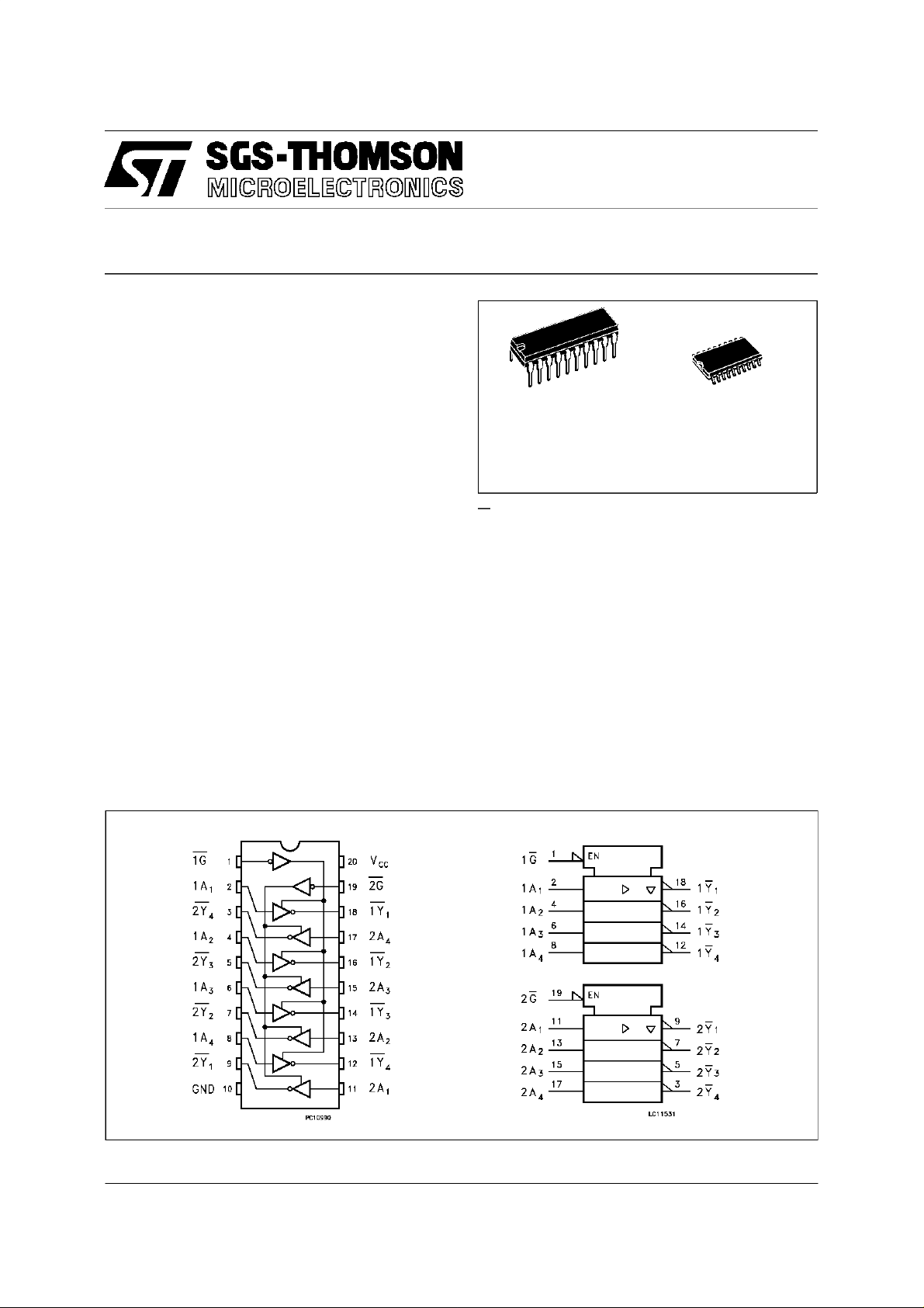
G controloutput governs four BUS BUFFERs.
This device is desibned to be used with 3 state
memoryaddress drivers,etc.
The device is designed to interface directly High
Speed CMOS systems with TTL, NMOS and
CMOSoutput voltage levels.
All inputs and outputs are equipped with
protectioncircuits against static discharge, giving
them 2KV ESD immunity and transient excess
voltage.
PINCONNECTION AND IEC LOGIC SYMBOLS
April 1997
1/8
Page 2
74ACT240
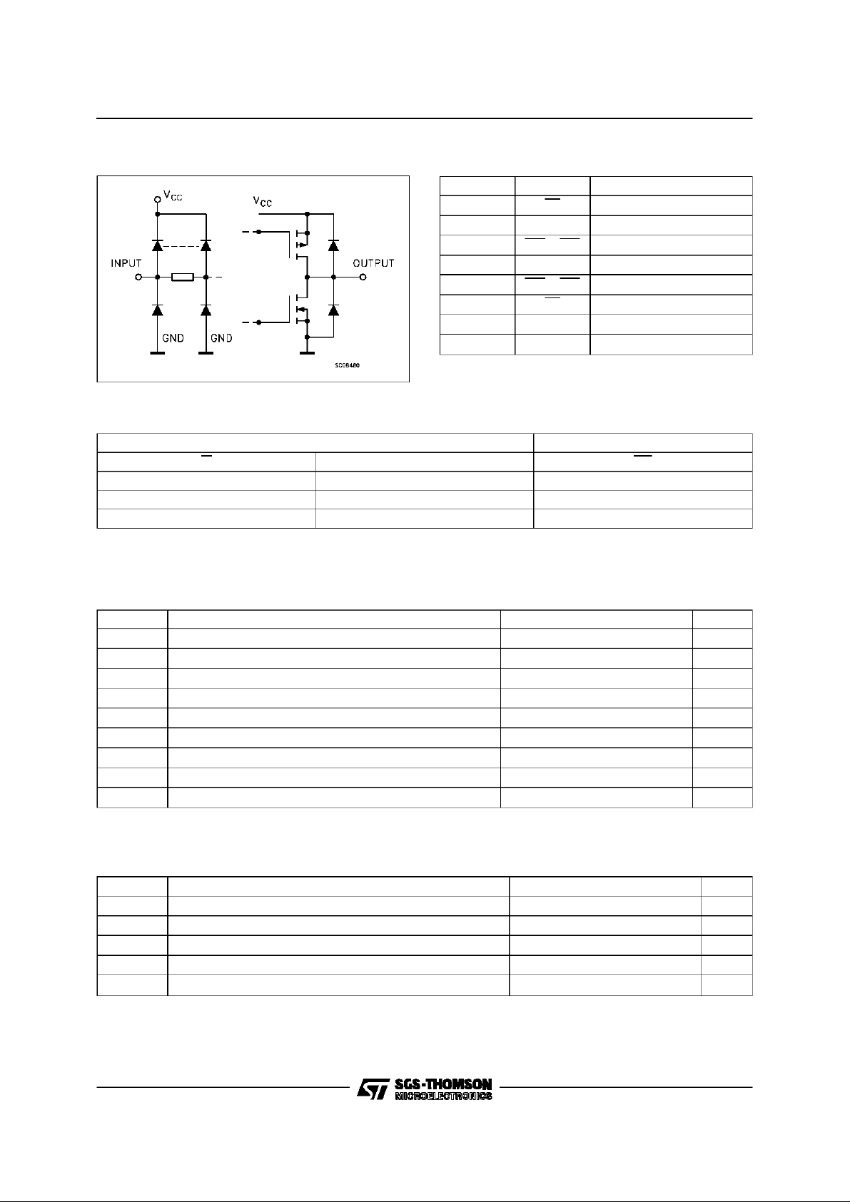
INPUTAND OUTPUTEQUIVALENTCIRCUIT
TRUTH TABLE
INPUT OUTPUT
GAnYn
LLH
LHL
HXZ
X:”H”or ”L”
Z: High impedance
PIN DESCRIPTION
PI N No SYM B O L NAME A ND FUNC T I ON
1 1G Output Enable Input
2,4,6,8 1A1to1A4 Data Inputs
9,7,5,3 2Y1to2Y4 Data Outputs
11,13,15, 17 2A1to2A4 Data Inputs
18,16,14, 12 1Y1to1Y4 Data Outputs
19 2G Output Enabel Input
10 GND Ground (0V)
20 V
CC
Positive Supply Voltage
ABSOLUTE MAXIMUM RATINGS
Symb o l Parame t er Val u e Uni t
V
V
V
I
I
OK
I
orI
I
CC
T
T
Absolute Maximum Ratings are those values beyond which damage to the device may occur. Functional operation under these condition is not implied.
Supply Voltage -0.5to+7 V
CC
DC Input Voltage -0.5toVCC+0.5 V
I
DC Output Voltage -0.5toVCC+0.5 V
O
DC Input Diode Current ± 20 mA
IK
DC Output Diode Current ± 20 mA
DC Output Current ± 50 mA
O
DC VCCor Ground Current ± 400 mA
GND
Storage Temperature -65to+150
stg
Lead Temperature (10 sec) 300
L
o
C
o
C
RECOMMENDEDOPERATINGCONDITIONS
Symbol Parameter Valu e Unit
V
V
V
T
dt/dv Input Rise and Fall Time V
1) VINfrom0.8Vto2.0V
Supply Voltage 4.5to5.5 V
CC
Input Voltage 0toV
I
Output Voltage 0toV
O
Operating Temperature: -40to+85
op
= 4.5 to 5.5V (note 1) 8 ns/V
CC
CC
CC
V
V
o
C
2/8
Page 3
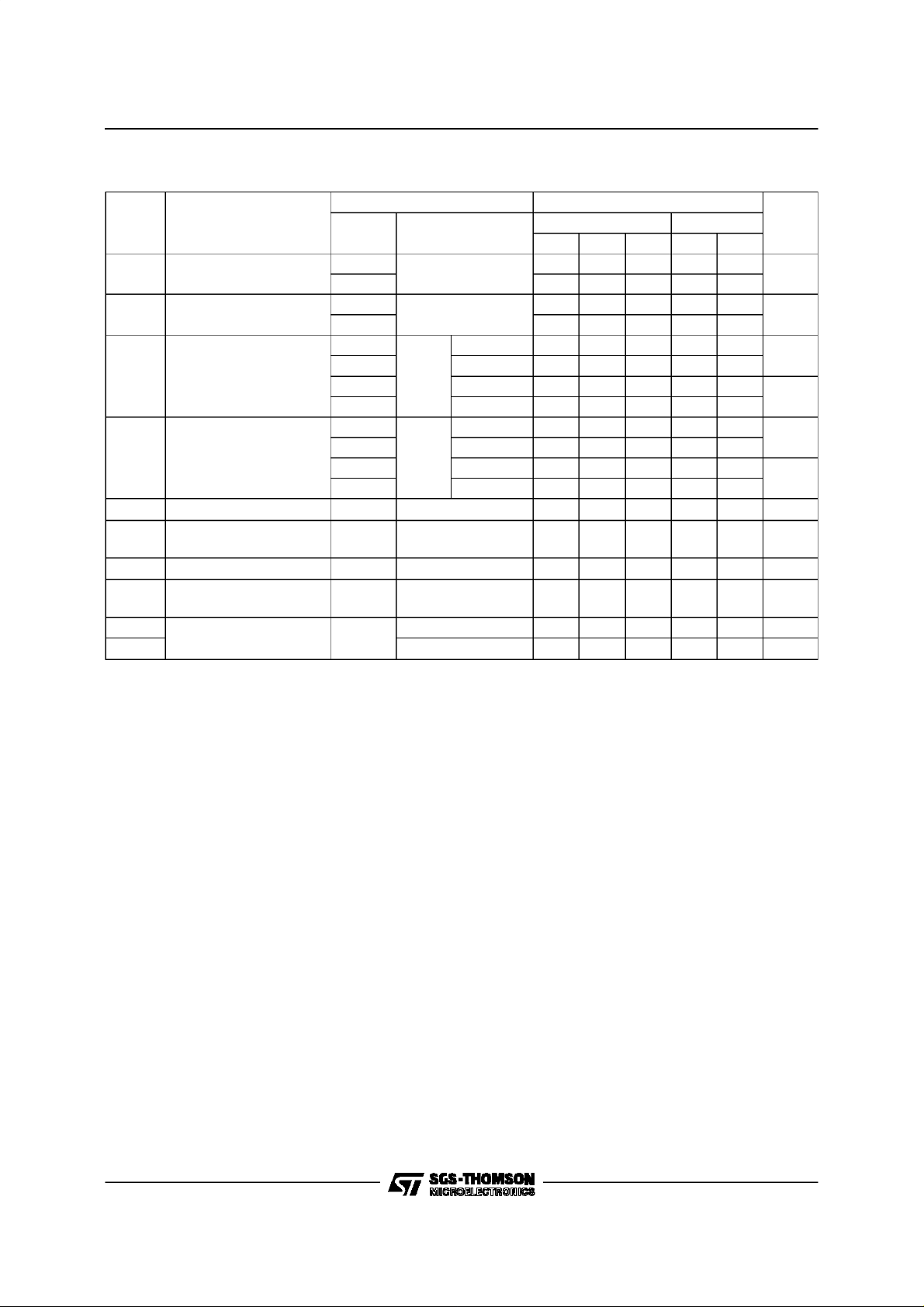
DC SPECIFICATIONS
74ACT240
Symbol Parameter Test Condit ions Value Unit
T
V
CC
(V)
High Level Input Voltage 4.5 VO=0.1V or
V
IH
5.5 2.0 1.5 2.0
Low Level Input Voltage 4.5 VO=0.1 Vor
V
IL
5.5 1.5 0.8 0.8
High Level Output
V
OH
Voltage
4.5
5.5 I
4.5 I
5.5 I
Low Level Output
V
OL
Voltage
4.5
5.5 I
4.5 I
5.5 I
Input Leakage Current
I
I
3 State Output Leakage
I
OZ
5.5
5.5 VI=VIHor V
Current
Max ICC/Input 5.5 VI=VCC-2.1V 0.6 1.5 mA
I
CCT
Quiescent Supply
I
CC
5.5 VI=VCCorGND 8 80 µA
V
-0.1 V
CC
-0.1 V
V
CC
IO=-50µA 4.4 4.49 4.4
(*)
=
V
I
V
or
IH
V
IL
(*)
V
I
or
V
IH
V
IL
=-50µA 5.4 5.49 5.4
O
=-24 mA 3.86 3.76
O
=-24 mA 4.86 4.76
O
IO=50µA0.0010.1 0.1
=
=50 mA 0.00 1 0.1 0.1
O
=24mA 0.36 0.44
O
=24mA 0.36 0.44
O
VI=VCCorGND ±0.1 ±1 µA
VO=VCCorGND
IL
=25oC-40to85
A
Min. Typ. Max. Min . Max.
2.0 1.5 2.0
1.5 0.8 0.8
±0.5 ±5 µA
o
C
Current
Dynamic Output Current
I
OLD
(note 1, 2)
I
OHD
1) Maximum testduration 2ms, one output loaded at time
2) Incident wave switching is guaranteed on transmission lines with impedances as low as 50 Ω.
(*)All outputs loaded.
5.5 V
=1.65 Vmax 75 mA
OLD
V
=3.85Vmin -75 mA
OHD
V
V
V
V
3/8
Page 4

74ACT240
AC ELECTRICAL CHARACTERISTICS (CL= 50 pF, RL=500 Ω, Inputtr=tf=3ns)
Symbol Parameter Test Cond itio n Value Unit
o
C
t
Propagation Delay Time 5.0
PLH
t
PHL
Output Enable Time 5.0
t
PZL
t
PZH
t
Output Disable Time 5.0
PLZ
t
PHZ
(*)Voltage range is 5V ± 0.5V
V
(V)
CC
T
=25oC-40to85
A
Min. Typ. Max. Min . Max.
(*)
(*)
(*)
1.55.07.51.58.5 ns
1.56.08.51.59.5 ns
1.5 6.5 10.0 1.5 10.5 ns
CAPACITIVE CHARACTERISTICS
Symbol Parameter Test Condit ions Value Unit
V
CC
(V)
Input Capacitance 5.0 4 pF
C
IN
C
Output Capacitance 5.0 8 pF
OUT
Power Dissipation
C
PD
5.0 21 pF
=25oC-40to85
T
A
Min. Typ. Max. Min . Max.
Capacitance (note 1)
1) CPDis defined as the value ofthe IC’s internal equivalent capacitance which is calculated from the operating current consumption without load. (Refer to
Test Circuit). Average operating current can be obtained by the following equation. I
(opr) =CPD• VCC•fIN+ICC/n (per circuit)
CC
o
C
TEST CIRCUIT
TEST SWITCH
t
PLH,tPHL
t
PZL,tPLZ
t
PZH,tPHZ
CL= 50 pF or equivalent (includes jig and probe capa citance)
R
= 500Ω or equivalent
L=R1
R
of pulse generator (typically 50Ω)
T=ZOUT
4/8
Open
2V
CC
Open
Page 5

WAVEFORM 1: PROPAGATIONDELAYS (f=1MHz;50% duty cycle)
74ACT240
WAVEFORM 2: OUTPUT ENABLE AND DISABLE TIME (f=1MHz; 50% duty cycle)
5/8
Page 6

74ACT240
Plastic DIP20 (0.25) MECHANICAL DATA
DIM.
MIN. TYP. MAX. MIN. TYP. MAX.
a1 0.254 0.010
B 1.39 1.65 0.055 0.065
b 0.45 0.018
b1 0.25 0.010
D 25.4 1.000
E 8.5 0.335
e 2.54 0.100
e3 22.86 0.900
F 7.1 0.280
I 3.93 0.155
L 3.3 0.130
Z 1.34 0.053
mm inch
6/8
P001J
Page 7

SO20 MECHANICAL DATA
74ACT240
DIM.
MIN. TYP. MAX. MIN. TYP. MAX.
A 2.65 0.104
a1 0.10 0.20 0.004 0.007
a2 2.45 0.096
b 0.35 0.49 0.013 0.019
b1 0.23 0.32 0.009 0.012
C 0.50 0.020
c1 45° (typ.)
D 12.60 13.00 0.496 0.512
E 10.00 10.65 0.393 0.419
e 1.27 0.050
e3 11.43 0.450
F 7.40 7.60 0.291 0.299
L 0.50 1.27 0.19 0.050
M 0.75 0.029
S8°(max.)
mm inch
P013L
7/8
Page 8

74ACT240
Information furnished is believed to be accurateand reliable. However, SGS-THOMSONMicroelectronics assumes no responsability for the
consequencesof use of such information nor for any infringement of patents or otherrights of third parties which may resultsfrom its use. No
licenseis granted byimplication or otherwise underany patent orpatent rightsof SGS-THOMSON Microelectronics. Specificationsmentioned
in this publicationare subject to change withoutnotice. This publication supersedes and replacesall information previously supplied.
SGS-THOMSONMicroelectronics productsare notauthorized for use ascriticalcomponents in lifesupportdevices or systems withoutexpress
writtenapproval of SGS-THOMSONMicroelectonics.
1997 SGS-THOMSONMicroelectronics- Printed in Italy - All Rights Reserved
Australia- Brazil - Canada- China- France- Germany - Hong Kong- Italy- Japan- Korea - Malaysia- Malta - Morocco - The Netherlands-
Singapore- Spain- Sweden- Switzerland - Taiwan- Thailand - United Kingdom - U.S.A
SGS-THOMSONMicroelectronics GROUP OF COMPANIES
.
8/8
 Loading...