

Datasheet 74ACT16543SSCX, 74ACT16543SSC, 74ACT16543MTDX, 74ACT16543MTD Datasheet (Fairchild Semiconductor)
Page 1
© 1999 Fairchild Semiconductor Corporation DS500301 www.fairchildsemi.com
August 1999
Revised October 1999
74ACT16543 16-Bit Registered Transceiver with 3-STATE Outputs
74ACT16543
16-Bit Registered Transceiver with 3-STATE Outputs
General Description
The ACT16543 cont ain s si xte en non -i nv ert in g t ran sceiv e rs
containing two sets of D-type registe rs for temporary storage of data flowing in either dir ecti o n. Each byte ha s sep arate control inputs wh ich can be shorted together for full
16-bit operation. Separate Latch Enable and Output
Enable inputs are provided for each register to permit independent input and o utput contr ol in either directio n of data
flow.
Features
■ Independent registers for A and B buses
■ Separate controls for data flow in each direction
■ Back-to-back registers for storage
Multiplexed real-time and stored data transfers
■ Separate control logic for each byte
■ Outputs source/sink 24 mA
■ TTL-compatible inputs
Ordering Code:
Device also available in Tape and Reel. Specify by appending s uffix let te r “X” to the ordering code.
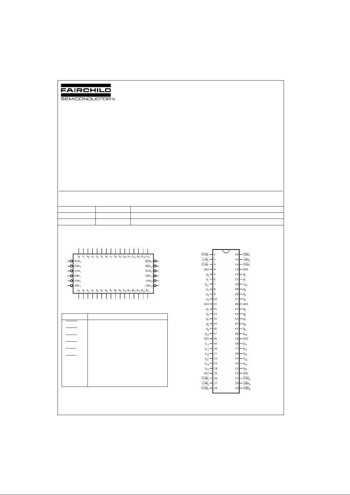
Logic Symbol
Pin Descriptions
Connection Diagram
FACT is a trade m ark of F airchild Semicondu ctor Corporation.
Order Number Package Number Package Description
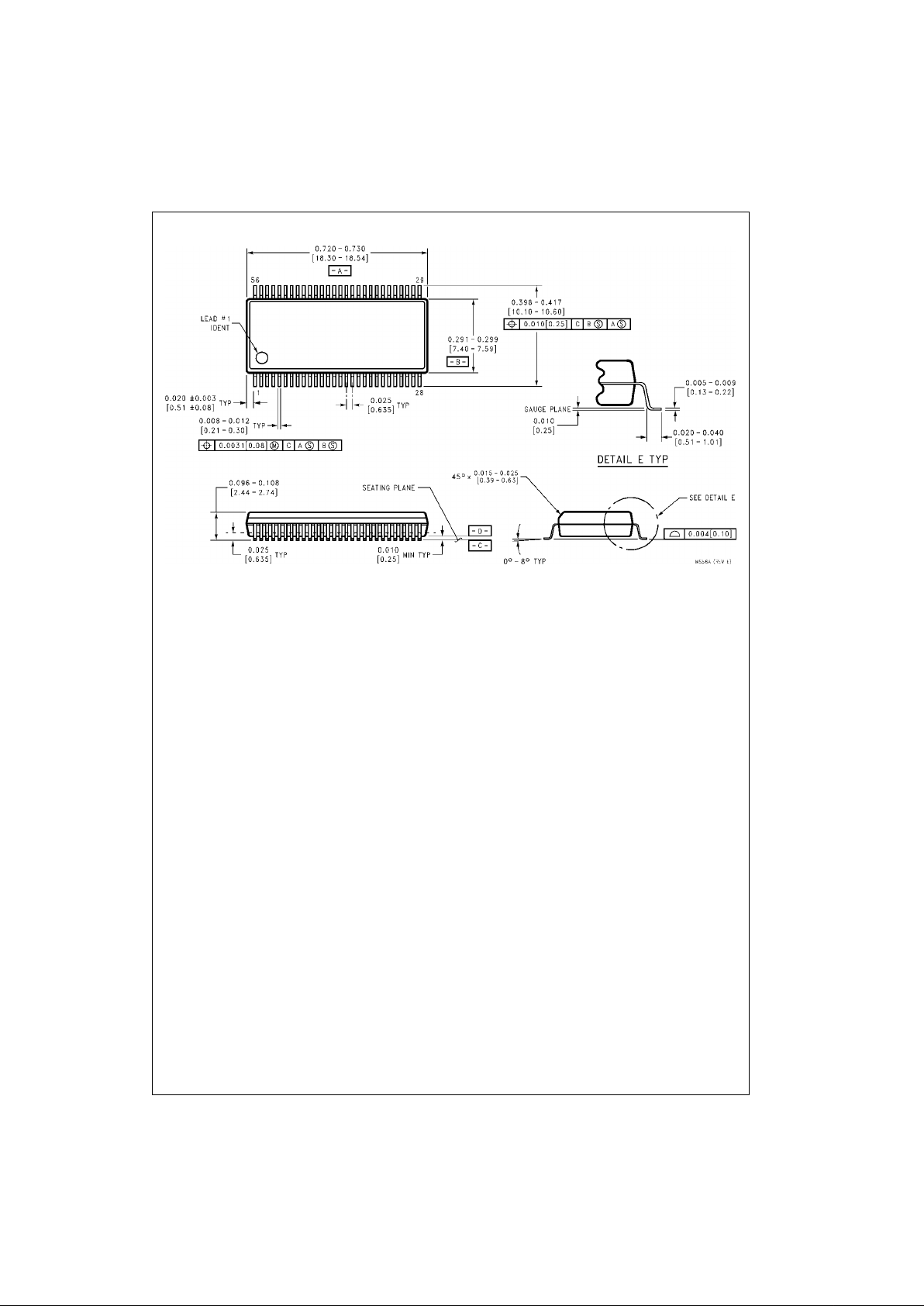
74ACT16543SSC MS56A 56-Lead Shrink Small Outline Package (SSOP), JEDEC MO-118, 0.300” Wide
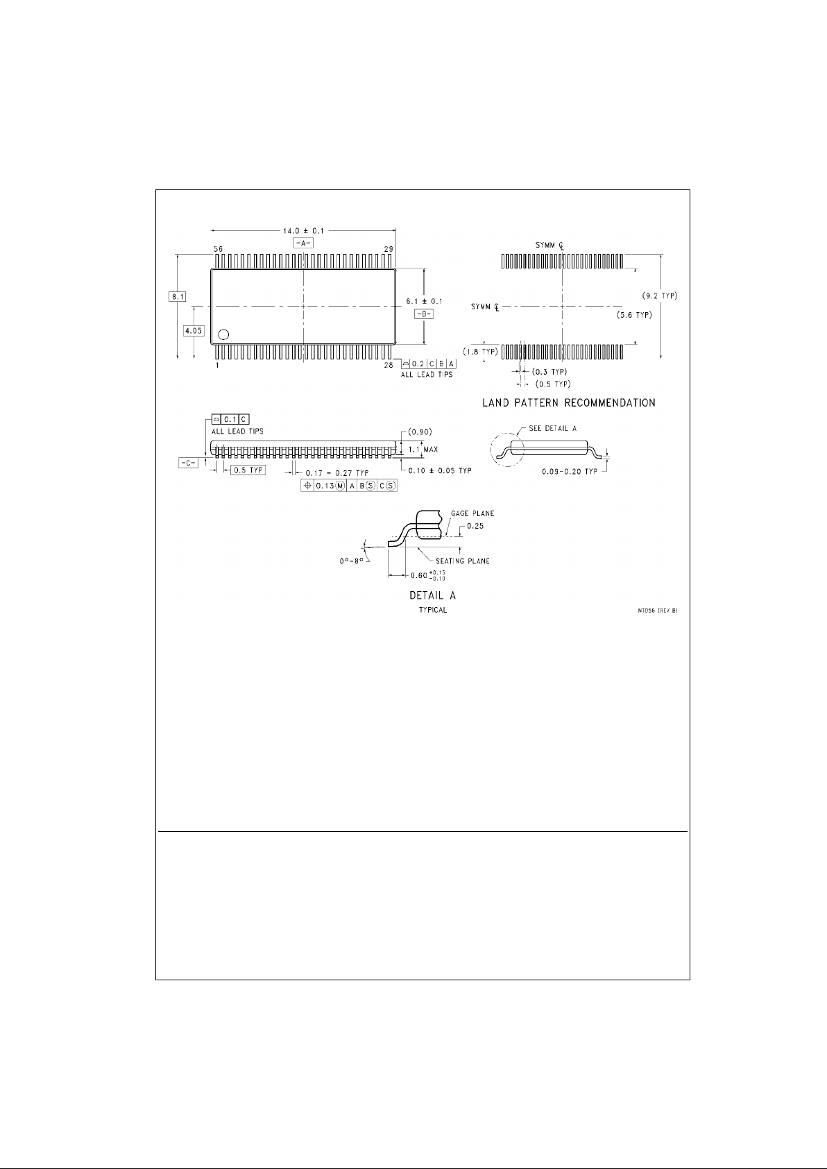
74ACT16543MTD MTD56 56-Lead Thin Shrink Small Outline Package (TSSOP), JEDEC MO-153, 6.1mm Wide
Pin Names Descriptions
OEAB
n
A-to-B Output Enable Input (Active LOW)
OEBA
n
B-to-A Output Enable Input (Active LOW)
CEAB
n
A-to-B Enable Input (Active LOW)
CEBA
n
B-to-A Enable Input (Active LOW)
LEAB
n
A-to-B Latch Enable Input (Active LOW)
LEBA
n
B-to-A Latch Enable Input (Active LOW)
A
0–A15
A-to-B Data Inputs or
B-to-A 3-STATE Outputs
B
0–B15
B-to-A Data Inputs or
A-to-B 3-STATE Outputs
Page 2
www.fairchildsemi.com 2
74ACT16543
Functional Description
The ACT16543 contains sixtee n non-inve rting tran sceivers
with 3-STAT E outputs. The device is byte controlled with
each byte functioning identically, but independent of the
other. The control pins may be shorted together to obta in
full 16-bit operat ion. The following description applies to
each byte. For data flow from A to B, for example, the A-toB Enable (CEAB
n
) input must be LOW in or der to enter
data from A
0–A15
or take data from B0–B15, as indicated in
the Data I/O Control Table. With CEAB
n
LOW, a LOW sig-
nal on the A-to-B Latch Enable (LEAB
n
) input makes the A-
to-B latches transparent; a subsequent LOW-to-HIGH transition of the LEAB
n
signal puts the A latche s i n the sto rage
mode and their outputs no longer change with the A inputs.
With CEAB
n
and OEABn both LOW, the 3-STATE B output
buffers are active and reflect the da ta p rese nt a t the output
of the A latches. Control of data flow from B to A is similar,
but using the CEBA
n
, LEBAn and OEBAn inputs.
Data I/O Control Table
H = HIGH Voltage Level
L = LOW Voltage Level
X = Immaterial
A-to-B data flow show n; B-to-A flow control
is the same, except using CEBA
n
, LEBAn and OEBA
n
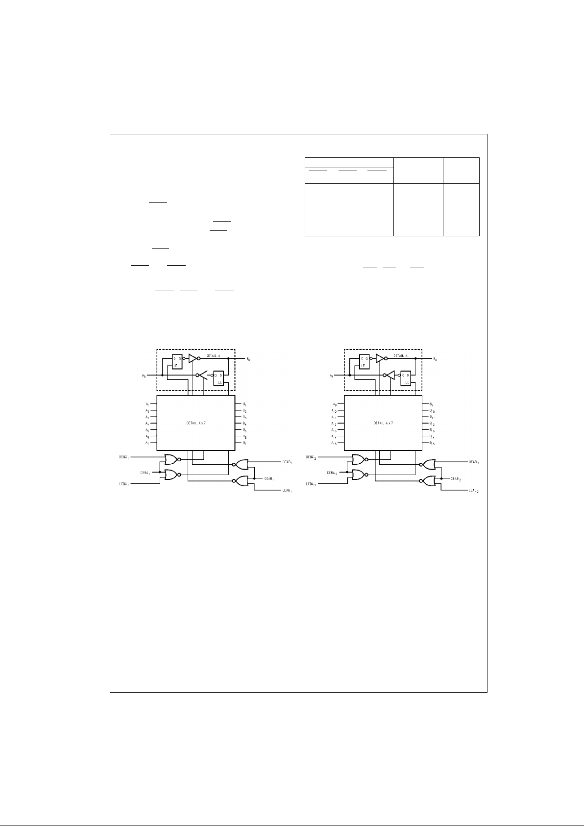
Logic Diagrams
Byte 1
(0:7)
Byte 2
(8:15)
Please note that this diagram is provided o nly f or t he understanding of lo gic operations and should not be used to estimate propagation delays.
Inputs Latch Status
(Byte n)
Output
Buffers
(Byte n)
CEAB
n
LEABnOEAB
n
H X X Latched High Z
X H X Latched —
L L X Transparent —
X X H — High Z
L X L — Driving
Page 3
3 www.fairchildsemi.com
74ACT16543
Absolute Maximum Ratings(Note 1) Recomm ended Operating
Conditions
Note 1: Absolute maximum ratings are those values beyond which damage
to the device may occur. The databook specifications should be met, without exception, to ensure that the system design is reliable over its power
supply, temperature, and ou tput/inp ut load ing vari ables. Fairchild does n ot
recommend operat ion of FACT circuits outside da t abook specifications.
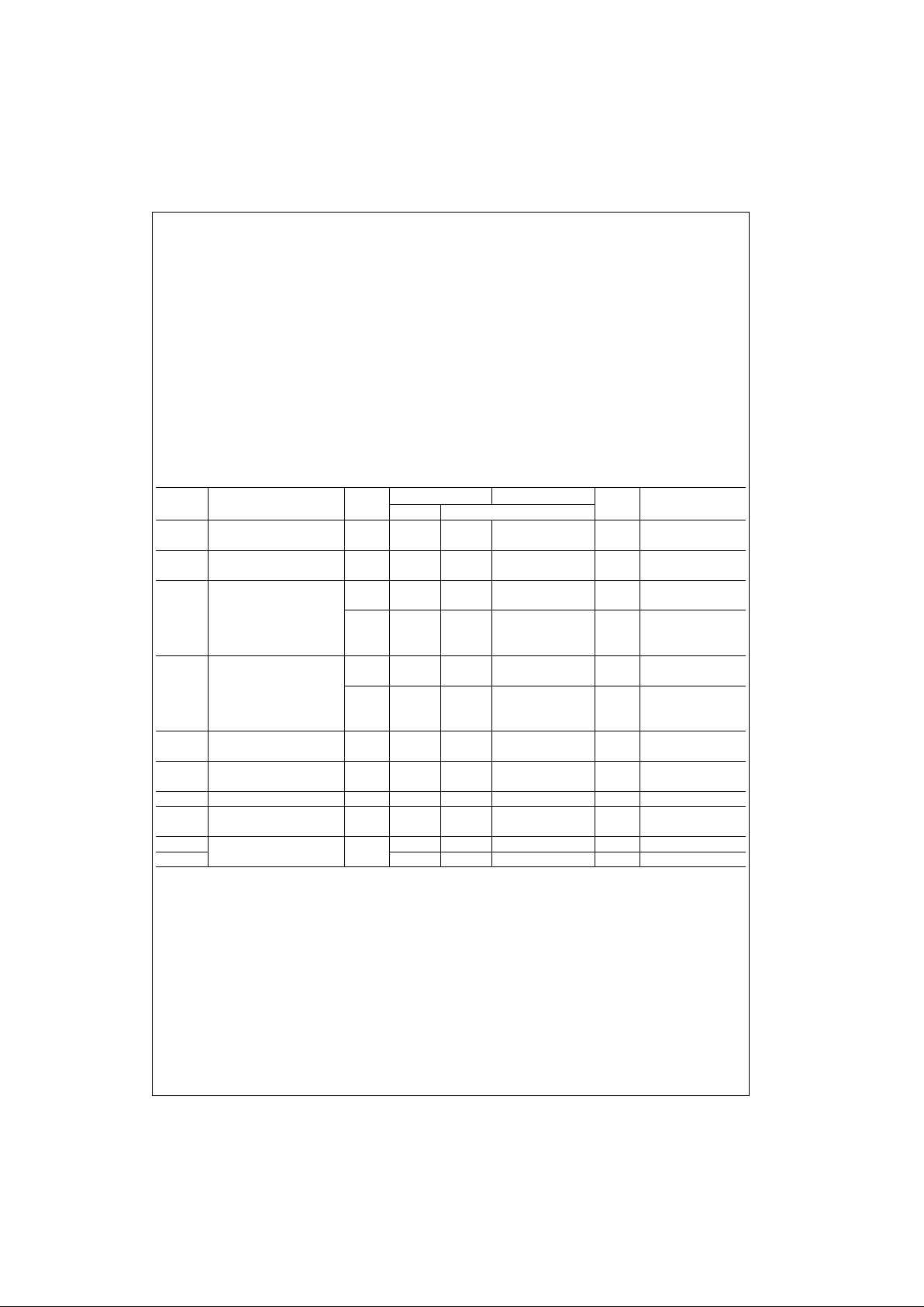
DC Electrical Characteristics
Note 2: All outputs loaded; thresholds assoc iated with output under t es t .
Note 3: Maximum test duration 2.0 ms; one output loaded at a time.
Supply Voltage (VCC) −0.5V to +7.0V
DC Input Diode Current (I
IK
)
V
I
= −0.5V −20 mA
V
I
= VCC + 0.5V +20 mA
DC Output Diode Current (I
OK
)
V
O
= −0.5V −20 mA
V
O
= VCC + 0.5V +20 mA
DC Output Voltage (V
O
) −0.5V to VCC + 0.5V
DC Output Source/Sink Current (I
O
) ±50 mA
DC V
CC
or Ground Current
per Output Pin ±50 mA
Storage Temperature −65°C to +150°C
Supply Voltage (V
CC
) 4.5V to 5.5V
Input Voltage (V
I
)0V to V
CC
Output Voltage (VO)0V to V
CC
Operating Temperature (TA) −40°C to +85°C
Minimum Input Edge Rate (∆V/∆t) 125 mV/ns
V
IN
from 0.8V to 2.0V
V
CC
@ 4.5V, 5.5V
Symbol Parameter
V
CC
TA = +25°CT
A
= −40°C to+85°C
Units Conditions
(V) Typ Guaranteed Limits
V
IH
Minimum HIGH 4.5 1.5 2.0 2 .0
V
V
OUT
= 0.1V
Input Voltage 5.5 1.5 2.0 2.0 or VCC − 0.1V
V
IL
Maximum LOW 4.5 1.5 0.8 0.8
V
V
OUT
= 0.1V
Input Voltage 5.5 1.5 0.8 0.8 or VCC − 0.1V
V
OH
Minimum HIGH 4.5 4.49 4.4 4.4
VI
OUT
= −50 µA
Output Voltage 5.5 5.49 5.4 5.4
VIN = VILor V
IH
4.5 3.86 3.76 V IOH = −24 mA
5.5 4.86 4.76 IOH = −24 mA (Note 2)
V
OL
Maximum LOW 4.5 0.001 0.1 0.1
V
I
OUT
= 50 µAOutput Voltage 5.5 0.001 0.1 0.1
VIN = VILor V
IH
4.5 0.36 0.44 V IOL = 24 mA
5.5 0.36 0.44 IOL = 24 mA (Note 2)
I
OZT
Maximum I/O
5.5 ±0.5 ±5.0 µA
VI = VIL, V
IH
Leakage Current VO = VCC, GND
I
IN
Maximum Input
5.5 ±0.1 ±1.0 µA
VI = VCC,
Leakage Current GND
I
CCT
Maximum ICC/Input 5.5 0.6 1.5 mA VI = VCC − 2.1V
I
CC
Max Quiescent
5.5 8.0 80.0 µA
VIN = V
CC
Supply Current or GND
I
OLD
Minimum Dynamic
5.5
75 mA V
OLD
= 1.65V Max
I
OHD
Output Current (Note 3) −75 mA V
OHD
= 3.85V Min
Page 4
www.fairchildsemi.com 4
74ACT16543
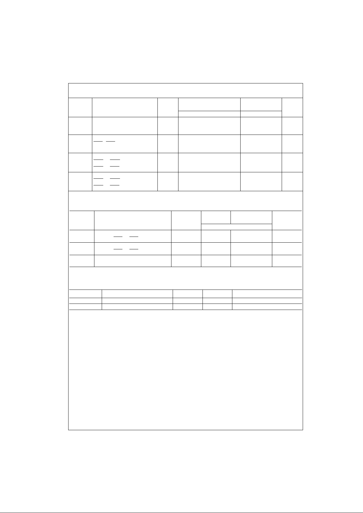
AC Electrical Characteristics
Note 4: Voltage Range 5.0 is 5. 0V ± 0.5V.
AC Operating Requirements
Note 5: Voltage Range 5.0 is 5. 0V ± 0.5V
Capacitance
V
CC
TA = +25°CT
A
= −40°C to +85°C
Symbol Parameter (V)
C
L
= 50 pF CL = 50 pF
Units
(Note 4) Min Typ Max Min Max
t
PLH
Propagation Delay 3.8 5.9 8.3 3.0 9.0
t
PHL
Transparent Mode 5.0 3.5 5.5 7.9 2.6 8.5 ns
An to Bnor Bn to A
n
t
PLH
Propagation Delay 4.7 6.9 9.8 3.4 10.8
t
PHL
LEBAn, LEAB
n
5.0
3.9 6.3 9.0 3.1 9.8
ns
to A
n
, B
n
t
PZH
Output Enable Time 4.2 6.3 9.2 3.0 9.9
t
PZL
OEBAn or OEABn to An or B
n
5.0
4.9 7.3 10.3 3.6 10.3
ns
CEBAn or CEABn to An or B
n
t
PHZ
Output Disable Time 2.8 5.2 8.0 2.1 8.3
t
PLZ
OEBAn or OEABn to An or B
n
5.0
2.6 5.0 7.6 2.0 8.1
ns
CEBAn or CEABn to An or B
n
V
CC
TA = +25°CTA = −40°C to +85°C
Symbol Parameter (V)
CL = 50 pF CL = 50 pF
Units
(Note 5) Guaranteed Minimum
t
S
Setup Time, HIGH or LOW
5.0 3.0 3.0 ns
An or Bn to LEBAn or LEAB
n
t
H
Hold Time, HIGH or LOW
5.0 1.5 1.5 ns
An or Bn to LEBAn or LEAB
n
t
W
Latch Enable, B to A
5.0 4.0 4.0 ns
Pulse Width, LOW
Symbol Parameter Typ Units Conditions
C
IN
Input Capacitance 4.5 pF VCC = 5.0V
C
PD
Power Dissipation.Capacitance 95.0 pF VCC = 5.0V
Page 5
5 www.fairchildsemi.com
74ACT16543
Physical Dimensions inches (millimeters) unless otherwise noted
56-Lead Thin Shrink Small Outline Package (SSOP), JEDEC MO-153, 6.1mm Wide
Package Number MS56A
Page 6
www.fairchildsemi.com 6
74ACT16543 16-Bit Registered Transceiver with 3-STATE Outputs
Physical Dimensions inches (millimeters) unless otherwise noted (Continued)
56-Lead Thin Shrink Small Outline Package (TSSOP), JEDEC MO-153, 6.1mm Wide
Package Number MTD56
Fairchild does not assume any responsibility for use of any circuitry described, no circuit pate nt licenses are implied and
Fairchild reserves the right at any time without notice to change said circuitry and specifications.
LIFE SUPPORT POLICY
FAIRCHILD’S PRODUCTS ARE NOT AUTHORIZED FOR USE AS CRITICAL COMPONENTS IN LIFE SUPPORT
DEVICES OR SYSTEMS WITHOUT THE EXPRESS WRITTEN APPROVAL OF THE PRESIDENT OF FAIRCHILD
SEMICONDUCTOR CORPORATION. As used herein:
1. Life support devices or systems are devices or syste ms
which, (a) are intended for surgical implant into the
body, or (b) support or sustain life, and (c) whose failure
to perform when properly used in accordance with
instructions for use provided in the labeling, can be reasonably expected to result in a significant inju ry to the
user.
2. A critical component i n any compon ent of a lif e support
device or system whose failu re to perform can be reasonably expected to ca use the fa i lure of the life su pp ort
device or system, or to affect its safety or effectiveness.
www.fairchildsemi.com
 Loading...