

Datasheet 74ACT16540SSCX, 74ACT16540SSC, 74ACT16540MTDX, 74ACT16540MTD Datasheet (Fairchild Semiconductor)
Page 1
© 1999 Fairchild Semiconductor Corporation DS500299 www.fairchildsemi.com
August 1999
Revised October 1999
74ACT16540 16-Bit Inverting Buffer/Line Driver with 3-STATE Outputs
74ACT16540
16-Bit Inverting Buffer/Line Driver with 3-STATE Outputs
General Description
The ACT16540 contain s sixteen inverting buffers with 3STATE outputs designed to be employed as a memory and
address driver, clock driver, or bus-oriented transmitter/
receiver. The device is byte controlled. Each byte has separate 3-STATE control inputs which can be shorted
together for full 16-bit operation.
Features
■ Separate control logic for each byte
■ Outputs source/sink 24 mA
■ TTL-compatible inputs
Ordering Code:
Device also available in Tape and Reel Specify by appending s uffix let t er “X” to the ordering code.
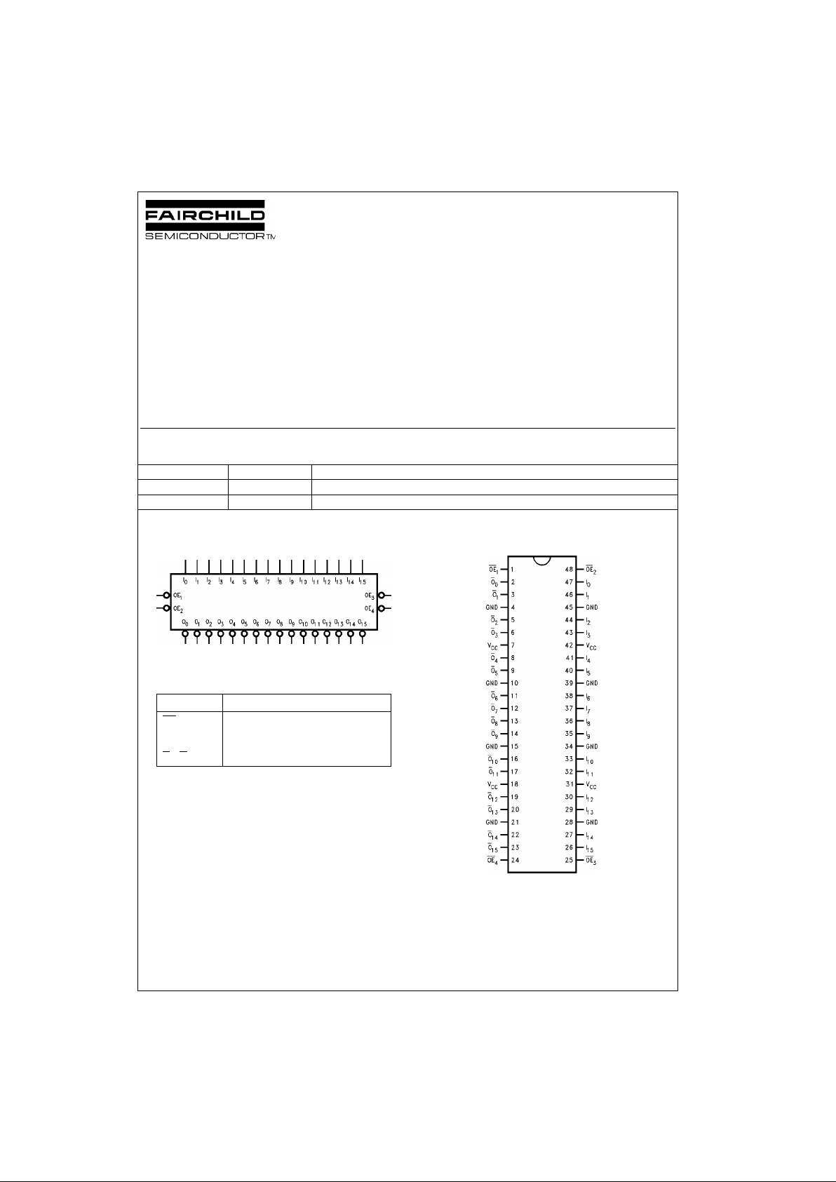
Logic Symbol
Pin Descriptions
Connection Diagram
FACT is a trade m ark of F airchild Semicondu ctor Corporation.
Order Number Package Number Package Description
74ACT16540SSC MS48A 48-Lead Small Shrink Outline Package (SSOP), JEDEC MO-118, 0.300” Wide
74ACT16540MTD MTD48 48-Lead Thin Shrink Small Outline Package (TSSOP), JEDEC MO-153, 6.1mm Wide
Pin Names Description
OE
n
Output Enable Input (Active LOW)
I
0–I15
Inputs
O
0–O15
Outputs
Page 2
www.fairchildsemi.com 2
74ACT16540
Functional Description
The ACT16540 contains sixteen inverting buffers with 3STATE standard outputs. The device is byte controlled with
each byte functioning identically, but independent of the
other. The control pins may be shorted together to obta in
full 16-bit operation. The 3-STA TE outputs are controlled by
an Output Enable (OE
n
) input for each byte. When OEn is
LOW, the outputs are in 2-state mode. When OE
n
is HIGH,
the outputs are in the high imp edance mode, b ut this do es
not interfere with entering new data into the inputs.
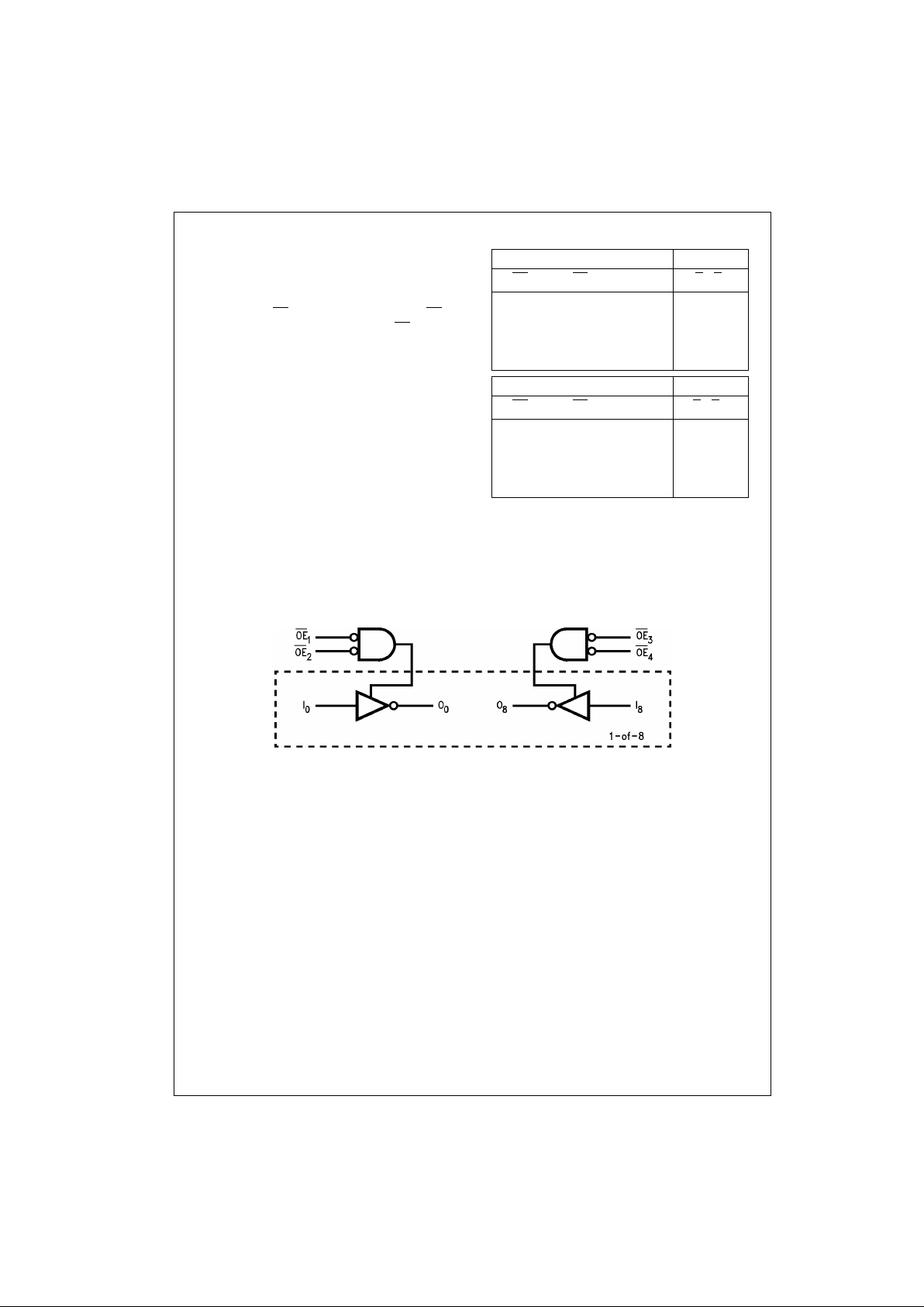
Tr uth Tables
H = HIGH Voltage Level
L = LOW Voltage Level
X = Immaterial
Z = High Impedance
Logic Diagram
Inputs Outputs
OE
1
OE
2
I0–I
7
O0–O
7
LLH L
HXX Z
XHX Z
LLL H
Inputs Outputs
OE
3
OE
4
I8–I
15
O8–O
15
LLH L
HXX Z
XHX Z
LLL H
Page 3
3 www.fairchildsemi.com
74ACT16540
Absolute Maximum Ratings(Note 1) Recommended Operating
Conditions
Note 1: Absolute maximum ratings are those values beyond which damage
to the device may occur. The databook specifications should be met, without exception to ensure that the system design is reliable over its power
supply, temperature, and ou tput/inp ut load ing vari ables. Fairchild does n ot
recommend operat ion of FACT circuits outside da t abook specifications.
DC Electrical Characteristics
Note 2: All outputs loaded; thresholds assoc iated with output under t es t .
Note 3: Maximum test duration 2.0 ms; one output loaded at a time.
Supply Voltage (VCC) −0.5V to +7.0V
DC Input Diode Current (I
IK
)
V
I
= −0.5V −20 mA
V
I
= VCC + 0.5V +20 mA
DC Output Diode Current (I
OK
)
V
O
= −0.5V −20 mA
V
O
= VCC + 0.5V +20 mA
DC Output Voltage (V
O
) −0.5V to VCC + 0.5V
DC Output Source/Sink Current (I
O
) ± 50 mA
DC V
CC
or Ground Current
per Output Pin ± 50 mA
Storage Temperature −65°C to +150°C
Supply Voltage (V
CC
) 4.5V to 5.5V
Input Voltage (V
I
)0V to V
CC
Output Voltage (VO)0V to V
CC
Operating Temperature (TA) −40°C to +85°C
Minimum Input Edge Rate (∆V/∆t) 125 mV/ns
V
IN
from 0.8V to 2.0V
V
CC
@ 4.5V, 5.5V
Symbol Parameter
V
CC
TA = +25°CT
A
= −40°C to +85°C
Units Conditions
(V) Typ Guaranteed Limits
V
IH
Minimum HIGH 4.5 1.5 2.0 2.0
V
V
OUT
= 0.1V
Input Voltage 5.5 1.5 2.0 2.0 or VCC − 0.1V
V
IL
Maximum LOW 4.5 1.5 0.8 0.8
V
V
OUT
= 0.1V
Input Voltage 5.5 1.5 0.8 0.8 or VCC − 0.1V
V
OH
Minimum HIGH 4.5 4.49 4.4 4.4
VI
OUT
= −50 µA
Output Voltage 5.5 5.49 5.4 5.4
VIN = VIL or V
IH
4.5 3.86 3.76 V IOH = −24 mA
5.5 4.86 4.76 IOH = −24 mA (Note 2)
V
OL
Maximum LOW 4.5 0.001 0.1 0.1
VI
OUT
= 50 µA
Output Voltage 5.5 0.001 0.1 0.1
VIN = VIL or V
IH
4.5 0.36 0.44 V IOL = 24 mA
5.5 0.36 0.44 IOL = 24 mA (Note 2)
I
OZ
Maximum 3-STATE
5.5 ± 0.5 ± 5.0 µA
VI = VIL, V
IH
Leakage Current VO = VCC, GND
I
IN
Maximum Input
5.5 ± 0.1 ± 1.0 µAVI = VCC, GND
Leakage Current
I
CCT
Maximum ICC/Input 5.5 0.6 1.5 mA VI = VCC − 2.1V
I
CC
Max Quiescent Supply Current 5.5 8.0 80.0 µAVIN = VCC or GND
I
OLD
Minimum Dynamic
5.5
75 mA V
OLD
= 1.65V Max
I
OHD
Output Current (Note 3) −75 mA V
OHD
= 3.85V Min
Page 4

www.fairchildsemi.com 4
74ACT16540
AC Electrical Characteristics
Note 4: Voltage Range 5.0 is 5. 0V ± 0.5V.
Capacitance
V
CC
TA = +25°CT
A
= −40°C to +85°C
Symbol Parameter (V)
C
L
= 50 pF CL = 50 pF
Units
(Note 4) Min Typ Max Min Max
t
PLH
Propagation Delay
5.0
2.7 4.9 7.3 2.7 7.8
ns
t
PHL
Data to Output 3.0 5.1 7.3 3.0 7.8
t
PZH
Output Enable
5.0
2.5 4.8 7.4 2.5 7.9
ns
t
PZL
Time 2.7 5.3 8.0 2.7 8.5
t
PHZ
Output Disable
5.0
2.5 5.4 8.3 2.5 8.7
ns
t
PLZ
Time 2.3 5.0 7.4 2.3 7.9
Symbol Parameter Typ Units Conditions
C
IN
Input Pin Capacitance 4.5 pF VCC = 5.0V
C
PD
Power Dissipation Capacitance 30 pF VCC = 5.0V
Page 5

5 www.fairchildsemi.com
74ACT16540
Physical Dimensions inches (millimeters) unless otherwise noted
48-Lead Small Shrink Outline Package (SSOP), JEDEC MO-118, 0.300” Wide
Package Number MS48A
Page 6

www.fairchildsemi.com 6
74ACT16540
Physical Dimensions inches (millimeters) unless otherwise noted (Continued)
48-Lead Thin Shrink Small Outline Package (TSSOP), JEDEC MO-153, 6.1mm Wide
Package Number MTD48
Page 7

7 www.fairchildsemi.com
74ACT16540 16-Bit Inverting Buffer/Line Driver with 3-STATE Outputs
Fairchild does not assume any responsibility for use of any circu itry described, no circuit patent license s are implied and
Fairchild reserves the right at any time without notice to change said circuitry and specifications.
LIFE SUPPORT POLICY
FAIRCHILD’S PRODUCTS ARE NOT AUTHORIZED FOR USE AS CRITICAL COMPONENTS IN LIFE SUPPORT
DEVICES OR SYSTEMS WITHOUT THE EXPRESS WRITTEN APPROVAL OF THE PRESIDENT OF FAIRCHILD
SEMICONDUCTOR CORPORATION. As used herein:
1. Life support devices or systems are dev ic es or syste ms
which, (a) are intended for surgical implant into the
body, or (b) support or sustain life, and (c) whose failure
to perform when properly used in accordance with
instructions for use provided i n the labe li ng, can be re asonably expected to result in a significant injury to the
user.
2. A critical component in any com ponen t of a life s uppor t
device or system whose failu re to perform can b e reasonably expected to c ause th e fa i lure of the li fe s upp or t
device or system, or to affect its safety or effectiveness.
www.fairchildsemi.com
 Loading...