

Page 1
74ACT16244
16-BIT BUS BUFFER
WITH 3 STATE OUTPUTS (NON INVERTED)
■ HIGHSPEED:t
■
LOW POWERDISSIPATION:
I
=8 µA (MAX.)at TA=25oC
CC
■
COMPATIBLEWITH TTLOUTPUTS
V
=2V(MIN),VIL=0.8V(MAX)
IH
■ 50Ω TRANSMISSIONLINEDRIVING
=4.8ns(TYP.)atVCC=5V
PD
CAPABILITY
■ SYMMETRICALOUTPUTIMPEDANCE:
|I
|=IOL=24mA(MIN)
OH
■ BALANCEDPROPAGAT IONDELAYS:
t
≅ t
PLH
PHL
■
OPERATINGVOLTAGERANGE:
V
(OPR)= 4.5Vto5.5V
CC
■ IMPROVEDLATCH-UPIMMUNITY
DESCRIPTION
The ACT16244 is an advanced CMOS 16-BIT
BUS BUFFER (3-STATE) fabricated with
sub-micron silicon gate and double-layer metal
wiringC
2
MOStechnology.
G output controlgovernsfourBUSBUFFERs.
The device is designed to be used with 3-state
memory address drivers, clock drivers, and
bus-oriented receivers and transmitters. The
devicecan be used as four 4-bit buffers, two 8-bit
buffers,or one 16-bit buffer.
The device is designed to interface directly High
Speed CMOS systems with TTL, NMOS and
CMOSoutputvoltage levels.
All inputs and outputs are equipped with
protection circuits against static discharge, giving
them 2KV ESD immunity and transient excess
voltage.
TSSOP
ORDER CODES
PACKAGE TUBE T & R
TSSOP 74ACT16244TTR
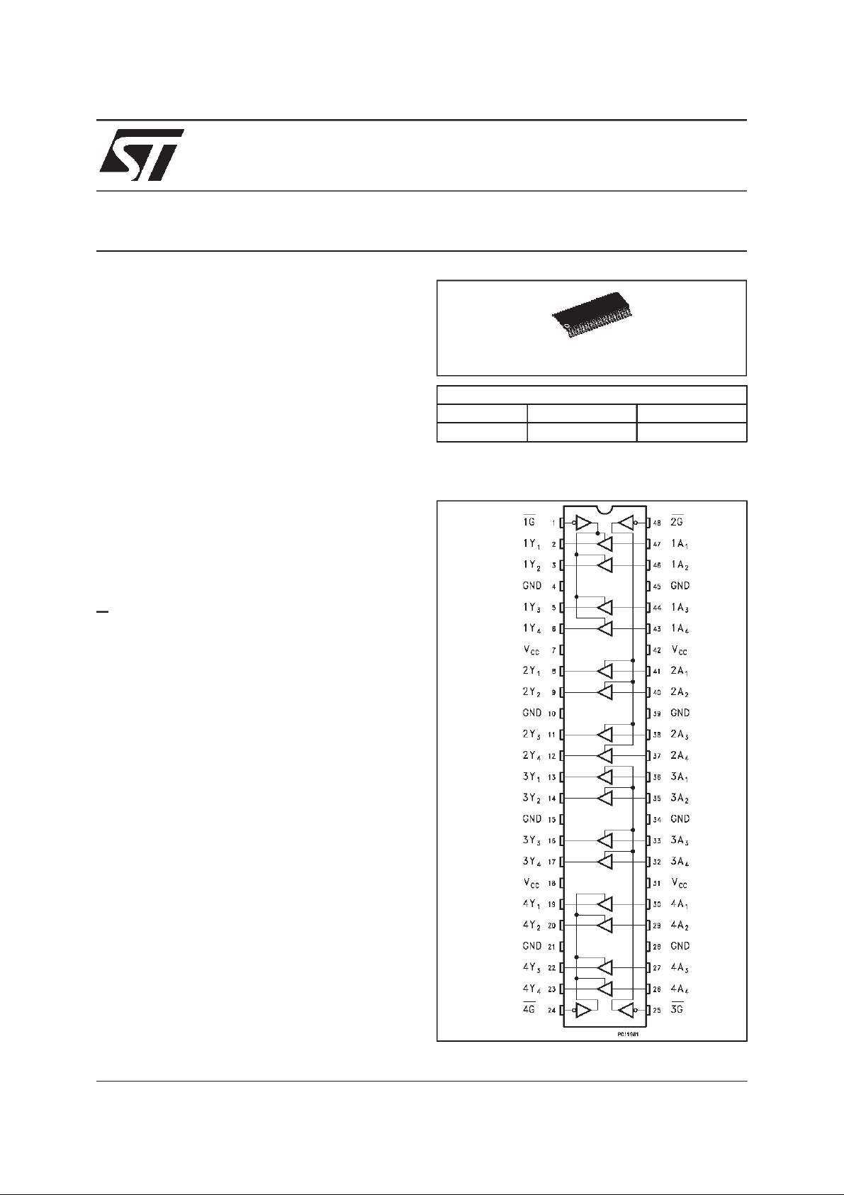
PIN CONNECTION
February 2000
1/8
Page 2
74ACT16244
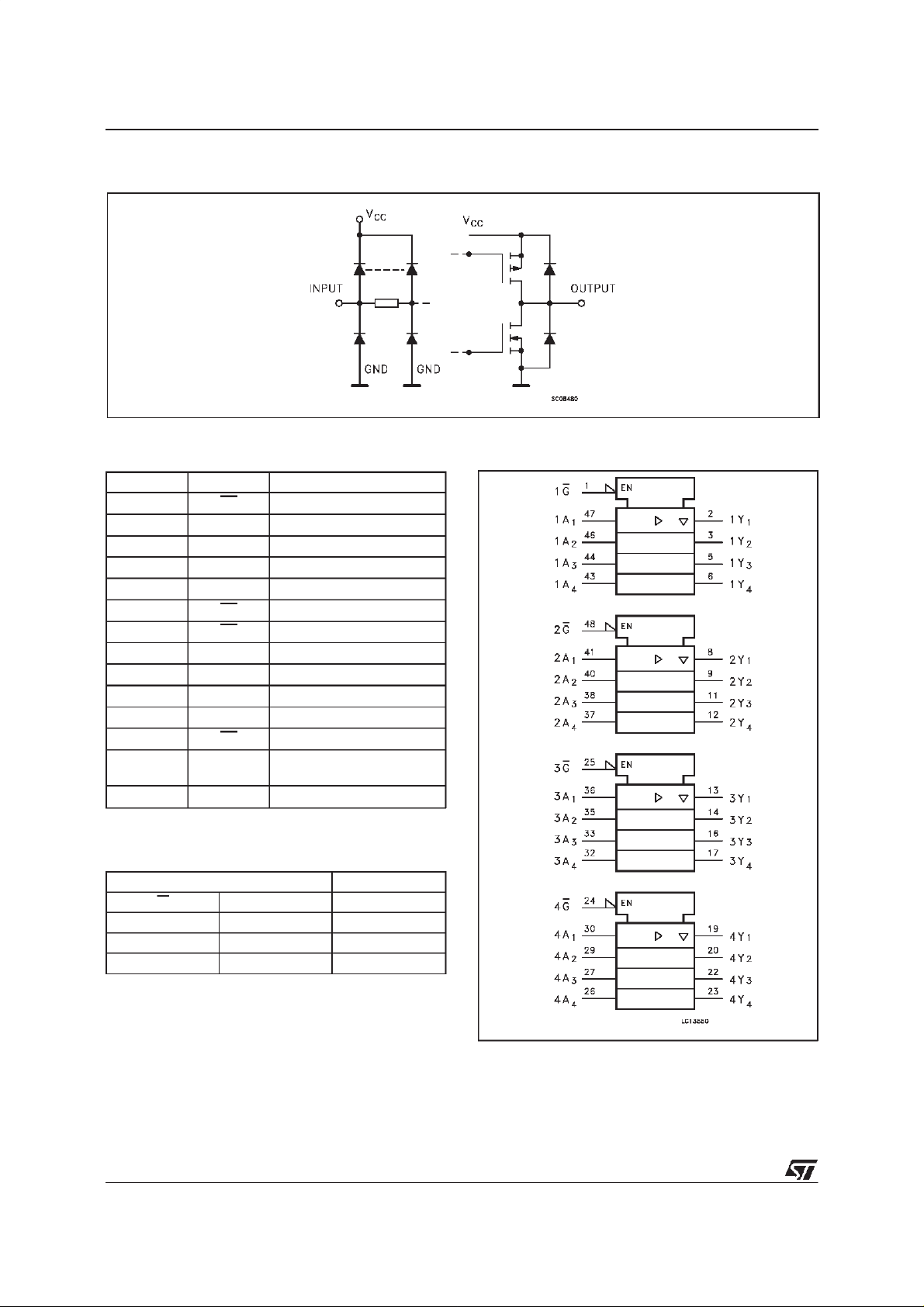
INPUT AND OUTPUTEQUIVALENT CIRCUIT
PI N No SYM BO L NAM E AN D FUNCTION
1 1G Output Enable Input
2,3,5,6 1Y1to 1Y4 Data Outputs
8,9,11, 12 2Y1to2Y4 Data Outputs
13,14,16,17 3Y1to 3Y4 Data Outputs
19,20,22,23 4Y1to 4Y4 Data Outputs
24 4G Output Enable Input
25 3G Output Enable Input
30,29,27,26 4A1to 4A4 Data Inputs
36,35,33,32 3A1to 3A4 Data Inputs
41,40,38,37 2A1to 2A4 Data Inputs
47,46,44,43 1A1to 1A4 Data Inputs
48 2G Output Enable Input
4,10,15,21,
28,34,39,45
7,18,31,42 V
GND Ground (0V)
CC
Positive Supply Voltage
IEC LOGICSYMBOLSPIN DESCRIPTION
TRUTH TABLE
INPUT OUTPU T
GAnYn
LLL
LHH
HXZ
X:”H” or”L”
Z:Highimpedance
2/8
Page 3
74ACT16244
ABSOLUTE MAXIMUM RATINGS
Symb o l Parameter Val u e Uni t
V
V
V
I
I
OK
I
orI
I
CC
T
T
AbsoluteMaximumRatingsarethosevaluesbeyond whichdamagetothedevicemayoccur. Functionaloperation underthese conditionisnotimplied.
RECOMMENDED OPERATINGCONDITIONS
Symb o l Parameter Val u e Uni t
V
V
V
T
dt/dv Input Rise and Fall Time V
1)VINfrom0.8V to2.0V
Supply Voltage -0.5to+7 V
CC
DC Input Voltage -0.5toVCC+0.5 V
I
DC Output Voltage -0.5toVCC+0.5 V
O
DC Input Diode Current ±20 mA
IK
DC Output Diode Current ±20 mA
DC Output Current
O
DC VCCor Ground Current
GND
Storage Temperature -65to+150
stg
Lead Temperature (10 sec) 300
L
Supply Voltage 4.5to5.5 V
CC
Input Voltage 0toV
I
Output Voltage 0toV
O
Operating Temperature: -40to+85
op
= 4.5 to 5.5V (note 1) 8 ns/V
CC
50 mA
±
400 mA
±
CC
CC
o
C
o
C
V
V
o
C
3/8
Page 4

74ACT16244
DC SPECIFICATIONS
Symbol Parameter Test Conditions Value Unit
T
V
CC
(V)
High Level Input Voltage 4.5 VO=0.1Vor
V
IH
5.5 2.0 2.0
Low Level Input Voltage 4.5 VO=0.1Vor
V
IL
5.5 0.8 0.8
High Level Output
V
OH
Voltage
4.5 IO=-50µA 4.4 4.49 4.4
5.5 I
4.5 I
5.5 I
Low Level Output
V
OL
Voltage
4.5 IO=50µA 0.001 0.1 0.1
5.5 I
4.5 I
5.5 I
Input Leakage Current 5.5 VI=VCCorGND ±0.1 ±1 µA
I
I
High Impedance Output
I
OZ
5.5 VI=VIHorV
Leakage Current
Max ICC/Input 5.5 VI=VCC-2.1V 0.9 1 mA
I
CCT
Quiescent Supply
I
CC
5.5 VI=VCCorGND 8 80 µA
-0.1V
V
CC
V
-0.1V
CC
=-50µA 5.4 5.49 5.4
O
=-24mA 3.94 3.8
O
=-24mA 4.94 4.8
O
=50mA 0.001 0.1 0.1
O
=24mA 0.36 0.44
O
=24mA 0.36 0.44
O
IL
VO=VCCorGND
Current
Dynamic Output Current
I
OLD
(note 1, 2)
I
OHD
1) Maximumtest duration 2ms, one output loaded attime
2)Incident waveswitchingisguaranteedontransmissionlines withimpedances aslowas50 Ω.
5.5 V
=1.65Vmax 75 mA
OLD
V
=3.85V min -75 mA
OHD
=25oC - 40 to 85oC
A
Min. Typ. Max. Min. Max.
2.0 2.0
0.8 0.8
±0.5 ±5 µA
V
V
V
V
4/8
Page 5

74ACT16244
AC ELECTRICAL CHARACTERISTICS (CL= 50 pF, RL= 500 Ω, Input tr=tf=3 ns)
Symbol Parameter Test Condition Value Unit
V
CC
(V)
t
Propagation Delay Time 5.0
PLH
t
PHL
Output Enable Time 5.0
t
PZL
t
PZH
t
Output Disable Time 5.0
PLZ
t
PHZ
(*)Voltagerange is5V±0.5V
(*)
(*)
(*)
CAPACITIVE CHARACTERISTICS
Symbol Parameter Test Conditions Value Unit
V
CC
(V)
C
Input Capacitance
IN
C
Output Capacitance
OUT
Power Dissipation
C
PD
Capacitance (note 1)
1)CPDisdefined as thevalueoftheIC’sinternalequivalentcapacitance whichis calculatedfromtheoperating currentconsumption without load.(Referto
TestCircuit).Average operatingcurrent canbeobtained bythefollowingequation.I
5.0
5.0
5.0 42 pF
(opr)= CPD• VCC• fIN+ICC/16(per circuit)
CC
T
=25oC - 40 to 85oC
A
Min. Typ. Max. Min. Max.
2.0 3.3 5.0 2.0 6.0 ns
3.0 4.8 6.5 3.0 8.0
4.0 6.5 8.7 4.0 9.7 ns
3.0 5.5 7.7 3.0 8.8
4.0 6.0 8.0 4.0 9.2 ns
3.0 4.6 6.4 3.0 7.3
=25oC - 40 to 85oC
T
A
Min. Typ. Max. Min. Max.
3.6
11
pF
pF
TESTCIRCUIT
TEST SWITCH
t
PLH,tPHL
t
PZL,tPLZ
t
PZH,tPHZ
CL= 50pFor equivalent (includes jigand probe capacitance)
=500Ωorequivalent
R
L=R1
R
ofpulsegenerator(typically50Ω)
T=ZOUT
Open
2V
CC
GND
5/8
Page 6

74ACT16244
WAVEFORM1: PROPAGATIONDELAYS
(f=1MHz;50%dutycicle)
WAVEFORM2: OUTPUT ENABLE AND DISABLE TIME(f=1MHz; 50% duty cicle)
6/8
Page 7

TSSOP48 MECHANICAL DATA
74ACT16244
DIM.
mm inch
MIN. TYP. MAX. MIN. TYP. MAX.
A 1.1 0.433
A1 0.05 0.10 0.15 0.002 0.004 0.006
A2 0.85 0.9 0.95 0.335 0.354 0.374
b 0.17 0.27 0.0067 0.011
c 0.09 0.20 0.0035 0.0079
D 12.4 12.5 12.6 0.408 0.492 0.496
E 7.95 8.1 8.25 0.313 0.319 0.325
E1 6.0 6.1 6.2 0.236 0.240 0.244
e 0.5 BSC 0.0197 BSC
K0
o
o
4
o
8
o
0
o
4
L 0.50 0.60 0.70 0.020 0.024 0.028
o
8
A2
A
A1
PIN 1 IDENTIFICATION
b
e
K
c
L
E
D
E1
1
7/8
Page 8

74ACT16244
Information furnished isbelieved tobe accurate andreliable. However, STMicroelectronics assumes no responsibility for the consequences
of use of such information nor for any infringement of patents or other rights of third parties which may result from its use. No license is
granted by implication or otherwise under any patent or patent rights of STMicroelectronics. Specification mentioned in this publication are
subject tochange without notice. Thispublicationsupersedes andreplaces all information previously supplied. STMicroelectronics products
are not authorized for use as criticalcomponents in lifesupport devices or systems withoutexpress written approval of STMicroelectronics.
The ST logo is a registeredtrademark of STMicroelectronics
2000 STMicroelectronics – Printed in Italy – All RightsReserved
STMicroelectronics GROUP OF COMPANIES
Australia - Brazil- China - Finland - France -Germany - Hong Kong - India - Italy - Japan- Malaysia -Malta - Morocco
Singapore - Spain- Sweden - Switzerland - United Kingdom - U.S.A.
http://www.st.com
.
8/8
 Loading...