

Page 1
SYNCHRONOUS PRESETTABLE 4-BIT COUNTER
■ HIGHSPEED:
=125MHz(TYP.)at VCC=5V
f
MAX
■ LOW POWER DISSIPATION:
=8 µA (MAX.) at TA=25oC
I
CC
■ COMPATIBLEWITHTTLOUTPUTS
=2V(MIN),VIL=0.8V(MAX)
V
IH
■ 50Ω TRANSMISSIONLINEDRIVING
CAPABILITY
■ SYMMETRICALOUTPUTIMPEDANCE:
|=IOL=24mA(MIN)
|I
OH
■ BALANCEDPROPAGATIONDELAYS:
≅ t
t
PLH
PHL
■ OPERATINGVOLTAGERANGE:
(OPR)= 4.5Vto 5.5V
V
CC
■ PINANDFUNCTIONCOMPATIBLEWITH
74SERIES161
■ IMPROVEDLATCH-UPIMMUNITY
DESCRIPTION
The ACT161 is a high-speed CMOS
SYNCRONOUS PRESETTABLE COUNTER
fabricated with sub-micron silicon gate and
double-layermetal wiring C
ideal for low power applications mantaining high
speed operation similar to eqivalent Bipolar
Schottky TTL. It is a 4 bit binary counter with
AsynchronousClear.
The circuit have four fundamental modes of
operation, in order of preference: synchronous
reset, parallel load, count-up and hold. Four
control inputs, Master Reset (CLEAR), Parallel
2
MOS technology.It is
74ACT161
B
(PlasticPackage)
(Micro Package)
ORDERCODES :
74ACT161B 74ACT161M
Enable Input (LOAD), Count Enable Input (PE)
and Count Enable Carry Input (TE), determine
the mode of operation as shown in the Truth
Table. A LOW signal on CLEAR overrides
counting and parallel loading and sets all outputs
on LOW state. A LOW signal on LOAD overrides
counting and allows information on Parallel Data
Qn inputs to be loaded into the flip-flops on the
next rising edge of CLOCK. With LOAD and
CLEAR, PE and TE permit counting when both
are HIGH. Conversely, a LOW signal on either
PE and TE inhibitscounting.
The device is designed to interface directly High
Speed CMOS systems with TTL, NMOS and
CMOSoutput voltagelevels.
All inputs and outputs are equipped with
protection circuits against static discharge, giving
them 2KV ESD immunity and transient excess
voltage.
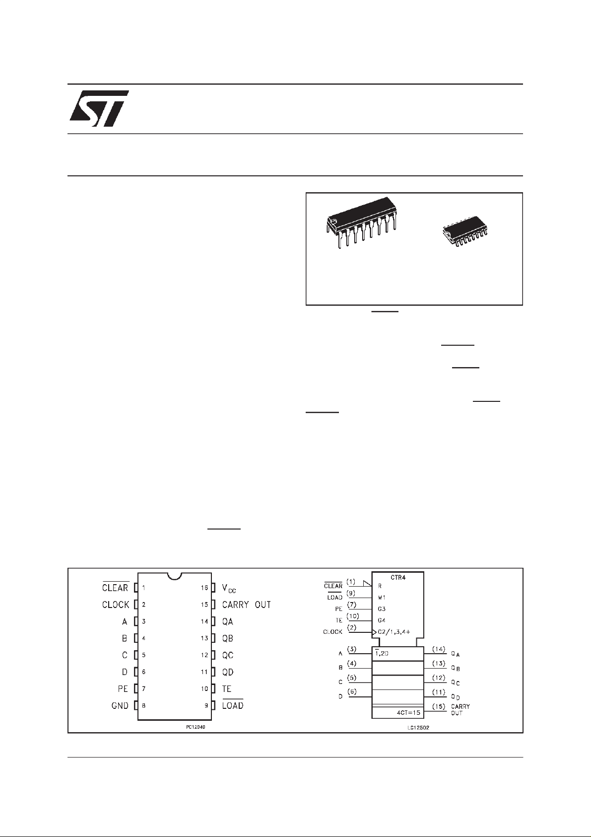
M
PIN CONNECTION AND IECLOGIC SYMBOLS
December 1998
1/11
Page 2
74ACT161
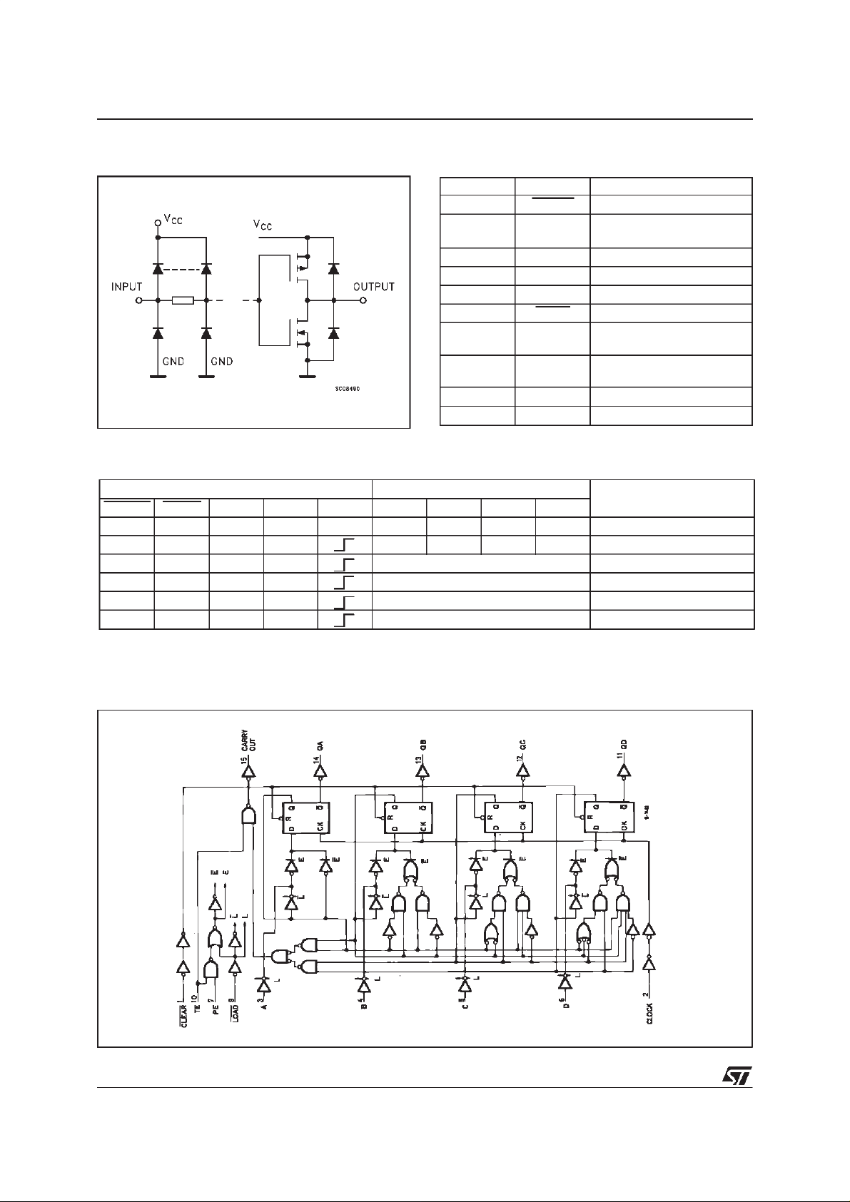
INPUT AND OUTPUTEQUIVALENTCIRCUIT
PIN DESCRIPTION
PI N No SYM BO L NAM E AND FU NCTION
1 CLEAR MasterReset
2 CLOCK ClockInput(LOW-to-HIGH,
Edge-Triggered)
3, 4, 5, 6 A, B, C, D Data Inputs
7 PE CountEnable Input
10 TE CountEnableCarryInput
9 LOAD Parallel EnableInput
14, 13,12,11QA to QD Flip-Flop Outpus
15 CARRY
OUT
8 GND Ground(0V)
16 V
CC
Terminal CountOutput
PositiveSupply Voltage
TRUTH TABLE
INPUTS OUTPUTS FUNCTION
CLEAR LOAD PE TE CL OCK QA QB QC QD
LXXXXLLLL RESET TO ”0”
H L X X A B C D PRESET DATA
H H X L NO CHANGE NO COUNT
H H L X NO CHANGE NO COUNT
H H H H COUNT UP COUNT
H X X X NO CHANGE NO COUNT
NOTE: X:Don’tCare
A,B, C,D: Logiclevelofdatainput
CARRY=TE • QA• QB• QC • QD
LOGICDIAGRAMS
2/11
Page 3
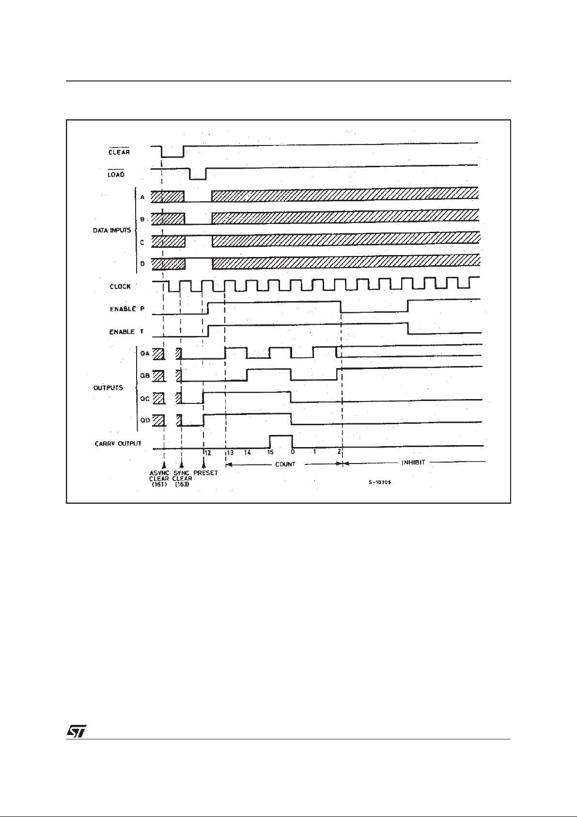
TIMINGCHART
74ACT161
3/11
Page 4
74ACT161
ABSOLUTE MAXIMUM RATINGS
Symb o l Para met er Val u e Uni t
V
V
V
I
I
OK
I
or I
I
CC
T
T
AbsoluteMaximumRatingsarethosevaluesbeyond whichdamage tothedevice mayoccur.Functionaloperation underthesecondition isnotimplied.
RECOMMENDEDOPERATINGCONDITIONS
Symb o l Paramet er Val u e Uni t
V
V
V
T
dt/dv InputRiseand FallTime V
1)VINfrom0.8V to2.0V
SupplyVoltage -0.5 to +7 V
CC
DC InputVoltage -0.5 to VCC+ 0.5 V
I
DC OutputVoltage -0.5 to VCC+ 0.5 V
O
DC InputDiode Current ± 20 mA
IK
DC OutputDiode Current ± 20 mA
DC OutputCurrent
O
DC VCCorGround Current
GND
Storage Temperature -65 to +150
stg
LeadTemperature (10 sec) 300
L
SupplyVoltage 4.5 to5.5 V
CC
InputVoltage 0 to V
I
OutputVoltage 0 to V
O
OperatingTemperature: -40 to +85
op
=4.5to5.5V(note1) 8 ns/V
CC
50 mA
±
300 mA
±
CC
CC
o
C
o
C
V
V
o
C
DC SPECIFICATIONS
Symbol Parameter Test Conditions Value Unit
=25oC -40 t o 85oC
V
CC
(V)
HighLevelInputVoltage 4.5 VO= 0.1V or
V
IH
5.5 2.0 1.5 2.0
LowLevel InputVoltage 4.5 VO= 0.1V or
V
IL
5.5 1.5 0.8 0.8
HighLevelOutputVoltage 4.5
V
OH
5.5 I
4.5 I
5.5 I
LowLevel OutputVoltage 4.5
V
OL
5.5 I
4.5 I
5.5 I
InputLeakage Current 5.5 VI=VCCor GND ±0.1 ±1 µA
I
I
MaxICC/Input 5.5 VI=VCC-2.1V 0.6 1.5 mA
I
CCT
Quiescent SupplyCurrent 5.5 VI=VCCor GND 4 40
I
CC
Dynamic OutputCurrent
I
OLD
OHD
(note 1, 2)
I
1) Maximum test duration 2ms,oneoutput loaded attime
2)Incident waveswitchingisguaranteed ontransmissionlines withimpedancesaslowas 50 Ω.
(*)Alloutputs loaded.
5.5 V
V
-0.1 V
CC
V
-0.1 V
CC
IO=-50 µA 4.4 4.49 4.4
(*)
=
V
I
V
IH
V
IL
(*)
V
I
V
IH
V
IL
OLD
V
OHD
=-50 µA 5.4 5.49 5.4
O
or
=-24 mA 3.86 3.76
O
=-24 mA 4.86 4.76
O
IO=50µA 0.001 0.1 0.1
=
=50 mA 0.001 0.1 0.1
O
or
=24 mA 0.36 0.44
O
=24 mA 0.36 0.44
O
= 1.65 V max 75 mA
= 3.85 V min -75 mA
T
A
Min. Typ. Max. Min. Max.
2.0 1.5 2.0
1.5 0.8 0.8
µ
V
V
V
V
A
4/11
Page 5

74ACT161
AC ELECTRICAL CHARACTERISTICS
= 50 pF, RL= 500 Ω, Inputtr=tf=3 ns)
(C
L
Symbol Parameter Test Condition Value Unit
t
PropagationDelay Time
PLH
t
CKto Q
PHL
PropagationDelay Time
t
PLH
CKto CARRYOUT
t
PHL
PropagationDelay Time
t
PLH
t
TEto CARRY OUT
PHL
PropagationDelay Time
t
PHL
CLEAR to CARRY OUT
CLRpulse Width,LOW 5.0
t
wL
CKpulse Width(LOAD)
t
w
HIGHor LOW
CKpulse Width(COUNT)
t
w
HIGHor LOW
SetupTime HIGH orLOW
t
s
(INPUTto CK)
HoldTimeHIGH or LOW
t
h
(INPUTto CK)
SetupTime HIGH orLOW
t
s
(LOADto CK)
HoldTimeHIGH or LOW
t
h
(LOADto CK)
SetupTime HIGH orLOW
t
s
(PEor TE to CK)
HoldTimeHIGH or LOW
t
h
(PEor TE to CK)
t
f
(*) Voltagerangeis5V ± 0.5V
RecoveryTime CLR to Q 5.0
REM
MaximumClock Frequency 5.0
MAX
V
(V)
5.0
5.0
5.0
5.0
5.0
5.0
5.0
5.0
5.0
5.0
5.0
5.0
CC
(*)
(*)
(*)
(*)
(*)
(*)
(*)
(*)
(*)
(*)
(*)
(*)
(*)
(*)
(*)
T
=25oC -40 t o 85oC
A
Min. Typ. Max. Min. Max.
1.5 5.5 9.5 10.5
1.5 7.0 11.0 12.0
1.5 5.5 8.5 10.0
1.5 6.0 10.0 11.0
2.5 3.0 7.5
2.0 3.0 3.5
2.0 3.0 3.5
1.5 9.5 11.5
-0.5 0 1.0
2.0 8.5 9.5
-2.0 -0.5 0
1.5 5.5 6.5
-2.0 0 0.5
-0.5 0.5 1.0
ns
ns
ns
ns
ns
ns
ns
ns
ns
ns
ns
ns
ns
ns
115 125 100 MHz
CAPACITIVE CHARACTERISTICS
Symbol Parameter Test Conditions Value Unit
T
V
CC
(V)
InputCapacitance
C
IN
C
PD
Power Dissipation
5.0
5.0 fIN= 10 MHz 45 pF
Capacitance (note1)
1)CPDisdefinedasthevalueoftheIC’sinternalequivalentcapacitance whichis calculated fromtheoperatingcurrent consumption without load. (Referto
TestCircuit).Average opertingcurrent canbeobtainedbythefollowingequation. I
(opr)=CPD• VCC• fIN+ICC/n(percircuit)
CC
=25oC -40 t o 85oC
A
Min. Typ. Max. Min. Max.
4.5
pF
5/11
Page 6

74ACT161
TESTCIRCUIT
CL= 50 pF orequivalent (includes jigand probe capacitance)
R
=500Ωorequivalent
L=R1
R
WAVEFORM1: PROPAGATIONDELAYS, COUNT MODE (f=1MHz; 50% duty cycle)
ofpulsegenerator (typically50Ω)
T=ZOUT
6/11
Page 7

74ACT161
WAVEFORM2: PROPAGATIONDELAYS CLEAR MODE
(f=1MHz;50% duty cycle)
WAVEFORM3: PROPAGATIONDELAYS PRESET MODE (f=1MHz;50% dutycycle)
7/11
Page 8

74ACT161
WAVEFORM4: PROPAGATIONDELAYS COUNTEABLEMODE
(f=1MHz;50% dutycycle)
WAVEFORM5: PROPAGATIONDELAYS CASCADE MODE (f=1MHz; 50%duty cycle)
8/11
Page 9

Plastic DIP-16 (0.25) MECHANICAL DATA
74ACT161
DIM.
MIN. TYP. MAX. MIN. TYP. MAX.
a1 0.51 0.020
B 0.77 1.65 0.030 0.065
b 0.5 0.020
b1 0.25 0.010
D 20 0.787
E 8.5 0.335
e 2.54 0.100
e3 17.78 0.700
F 7.1 0.280
I 5.1 0.201
L 3.3 0.130
Z 1.27 0.050
mm inch
P001C
9/11
Page 10

74ACT161
SO-16 MECHANICALDATA
DIM.
MIN. TYP. MAX. MIN. TYP. MAX.
A 1.75 0.068
a1 0.1 0.2 0.004 0.007
a2 1.65 0.064
b 0.35 0.46 0.013 0.018
b1 0.19 0.25 0.007 0.010
C 0.5 0.019
c1 45 (typ.)
D 9.8 10 0.385 0.393
E 5.8 6.2 0.228 0.244
e 1.27 0.050
e3 8.89 0.350
F 3.8 4.0 0.149 0.157
G 4.6 5.3 0.181 0.208
L 0.5 1.27 0.019 0.050
M 0.62 0.024
S 8 (max.)
mm inch
10/11
P013H
Page 11

74ACT161
Information furnished is believed to be accurate and reliable. However, STMicroelectronics assumes no responsibility forthe consequences
of use of such information nor for any infringement of patents or other rights of third parties which may result from its use. No license is
granted by implicationor otherwise under any patent or patent rights of STMicroelectronics. Specification mentioned in this publication are
subject tochange without notice. This publication supersedes and replaces all information previously supplied. STMicroelectronics products
are not authorized for use as critical components in life support devices or systems without express written approval of STMicroelectronics.
The ST logo is a registered trademark of STMicroelectronics
1998 STMicroelectronics – Printed in Italy – All Rights Reserved
STMicroelectronics GROUP OF COMPANIES
Australia - Brazil -Canada -China -France - Germany - Italy - Japan -Korea - Malaysia - Malta - Mexico -Morocco - The Netherlands -
Singapore - Spain -Sweden - Switzerland - Taiwan - Thailand - UnitedKingdom -U.S.A.
http://www.st.com
.
11/11
 Loading...