

Page 1
54AC/74AC139#54ACT/74ACT139
Dual 1-of-4 Decoder/Demultiplexer
54AC/74AC139
February 1993
General Description
The ’AC/’ACT139 is a high-speed, dual 1-of-4 decoder/demultiplexer. The device has two independent decoders,
each accepting two inputs and providing four mutually-exclusive active-LOW outputs. Each decoder has an activeLOW Enable input which can be used as a data input for a
4-output demultiplexer. Each half of the ’AC/’ACT139 can
be used as a function generator providing all four minterms
of two variables.
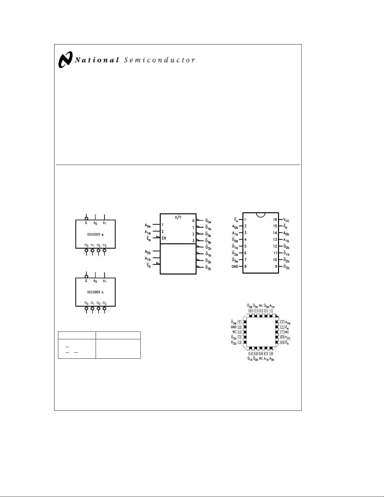
Logic Symbols
IEEE/IEC
TL/F/9926– 8
Features
Y
ICCreduced by 50%
Y
Multifunction capability
Y
Two completely independent 1-of-4 decoders
Y
Active LOW mutually exclusive outputs
Y
Outputs source/sink 24 mA
Y
’ACT139 has TTL-compatible inputs
Y
Standard Military Drawing (SMD)
Ð’AC139: 5962-87623
Ð’ACT139: 5962-87553
Connection Diagrams
Pin Assignment
for DIP, Flatpak and SOIC
TL/F/9926– 2
#
54ACT/74ACT139 Dual 1-of-4 Decoder/Demultiplexer
TL/F/9926– 3
Pin Assignment
for LCC
TL/F/9926– 1
Pin Names Description
A0,A
1
E
O
0–O3
FACTTMis a trademark of National Semiconductor Corporation.
C
1995 National Semiconductor Corporation RRD-B30M75/Printed in U. S. A.
Address Inputs
Enable Inputs
Outputs
TL/F/9926– 4
TL/F/9926
Page 2
Functional Description
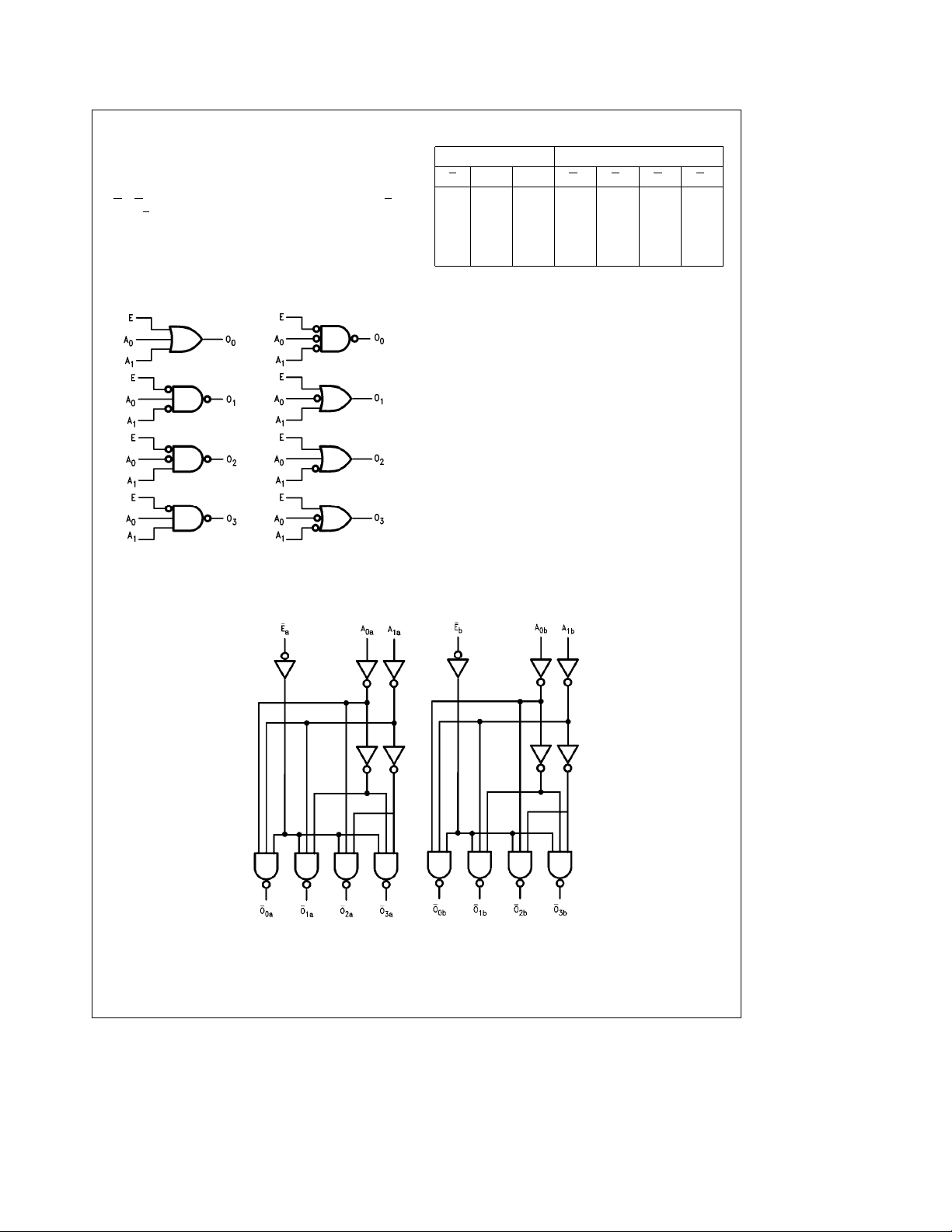
The ’AC/’ACT139 is a high-speed dual 1-of-4 decoder/demultiplexer. The device has two independent decoders,
each of which accepts two binary weighted inputs (A
and provides four mutually exclusive active-LOW outputs
(O
). Each decoder has an active-LOW enable (E).
0–O3
When E
is HIGH all outputs are forced HIGH. The enable
can be used as the data input for a 4-output demultiplexer
application. Each half of the ’AC/’ACT139 generates all four
minterms of two variables. These four minterms are useful
in some applications, replacing multiple gate functions as
shown in
Figure a
, and thereby reducing the number of
packages required in a logic network.
0–A1
)
Truth Table
Inputs Outputs
E A
HXXHHHH
LLLLHHH
LHLHLHH
LLHHHLH
LHHHHHL
e
H
HIGH Voltage Level
e
LOW Voltage Level
L
e
Immaterial
X
A
O
O
O
0
1
0
1
O
2
3
FIGURE a. Gate Functions (Each Half)
TL/F/9926– 6
Logic Diagram
Please note that this diagram is provided only for the understanding of logic operations and should not be used to estimate propagation delays.
TL/F/9926– 5
2
Page 3
Absolute Maximum Rating (Note 1)
If Military/Aerospace specified devices are required,
please contact the National Semiconductor Sales
Office/Distributors for availability and specifications.
b
0.5V to V
b
0.5V to V
b
0.5V toa7.0V
b
a
a
CC
b
a
a
CC
20 mA
20 mA
0.5V
20 mA
20 mA
0.5V
Supply Voltage (V
DC Input Diode Current (IIK)
eb
V
0.5V
I
e
V
V
I
CC
)
CC
a
0.5V
DC Input Voltage (VI)
DC Output Diode Current (IOK)
eb
V
0.5V
O
e
V
O
a
V
0.5V
CC
DC Output Voltage (VO)
DC Output Source
or Sink Current (I
)
O
g
50 mA
DC VCCor Ground Current
per Output Pin (I
Storage Temperature (T
Junction Temperature (T
CDIP 175
CC
or I
GND
STG
J
)
)
b
)
PDIP 140
Note 1: Absolute maximum ratings are those values beyond which damage
to the device may occur. The databook specifications should be met, without
exception, to ensure that the system design is reliable over its power supply,
temperature, and output/input loading variables. National does not recom-
mend operation of FACT
TM
circuits outside databook specifications.
g
50 mA
65§Ctoa150§C
C
§
C
§
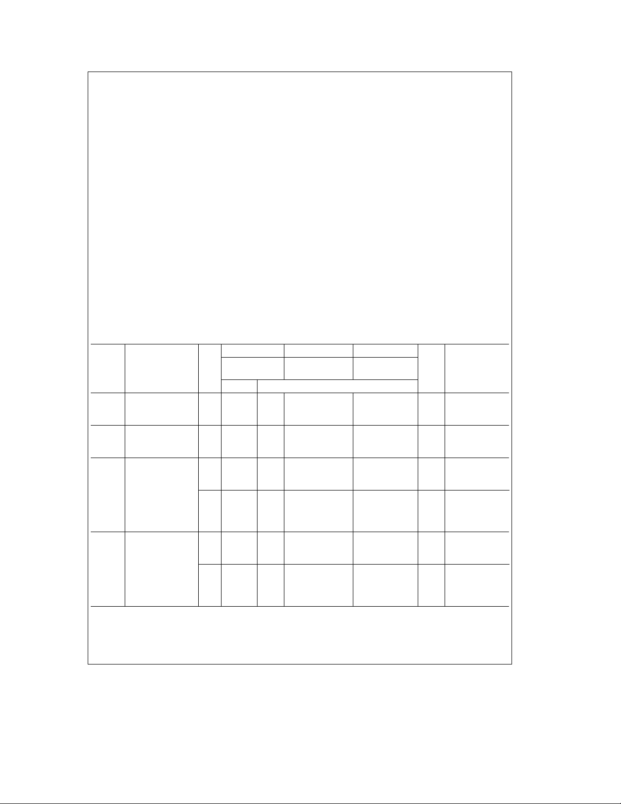
DC Characteristics for ’AC Family Devices
74AC 54AC 74AC
V
Symbol Parameter
V
Minimum High Level 3.0 1.5 2.1 2.1 2.1 V
IH
Input Voltage 4.5 2.25 3.15 3.15 3.15 V or V
(V)
CC
5.5 2.75 3.85 3.85 3.85
V
Maximum Low Level 3.0 1.5 0.9 0.9 0.9 V
IL
Input Voltage 4.5 2.25 1.35 1.35 1.35 V or V
5.5 2.75 1.65 1.65 1.65
V
Minimum High Level 3.0 2.99 2.9 2.9 2.9 I
OH
Output Voltage 4.5 4.49 4.4 4.4 4.4 V
5.5 5.49 5.4 5.4 5.4
3.0 2.56 2.4 2.46
4.5 3.86 3.7 3.76 V I
5.5 4.86 4.7 4.76
V
Maximum Low Level 3.0 0.002 0.1 0.1 0.1 I
OL
Output Voltage 4.5 0.001 0.1 0.1 0.1 V
5.5 0.001 0.1 0.1 0.1
3.0 0.36 0.50 0.44 12 mA
4.5 0.36 0.50 0.44 V I
5.5 0.36 0.50 0.44 24 mA
*All outputs loaded; thresholds on input associated with output under test.
ea
T
25§C
A
b
55§Ctoa125§Cb40§Ctoa85§C
Typ Guaranteed Limits
Recommended Operating
Conditions
Supply Voltage (VCC)
’AC 2.0V to 6.0V
’ACT 4.5V to 5.5V
Input Voltage (V
Output Voltage (VO) 0VtoV
Operating Temperature (TA)
74AC/ACT
54AC/ACT
Minimum Input Edge Rate (DV/Dt)
’AC Devices
V
from 30% to 70% of V
IN
V
CC
Minimum Input Edge Rate (DV/Dt)
’ACT Devices
V
from 0.8V to 2.0V
IN
V
CC
e
T
A
) 0VtoV
I
b
40§Ctoa85§C
b
55§Ctoa125§C
@
3.3V, 4.5V, 5.5V 125 mV/ns
@
4.5V, 5.5V 125 mV/ns
CC
e
T
A
Units Conditions
e
OUT
b
CC
e
OUT
b
CC
eb
OUT
e
*V
VILor V
IN
OH
e
50 mA
OUT
e
*V
VILor V
IN
OL
0.1V
0.1V
b
b
b
0.1V
0.1V
50 mA
12 mA
24 mA
24 mA
24 mA
CC
CC
IH
IH
3
Page 4
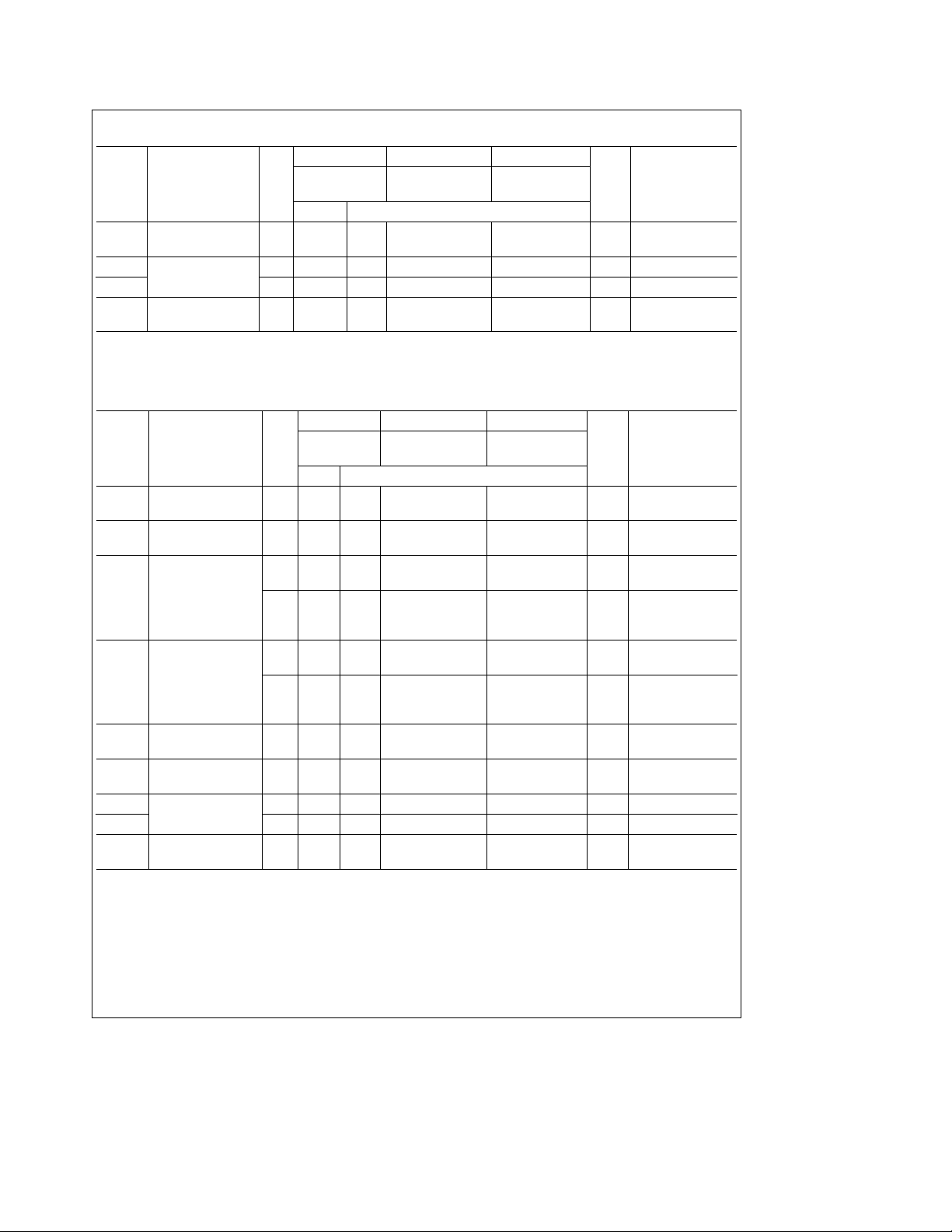
DC Characteristics for ’AC Family Devices (Continued)
74AC 54AC 74AC
Symbol Parameter
V
(V)
CC
T
A
ea
25§C
b
e
T
A
55§Ctoa125§Cb40§Ctoa85§C
Typ Guaranteed Limits
I
IN
I
OLD
I
OHD
I
CC
Maximum Input
Leakage Current
²
Minimum Dynamic 5.5 50 75 mA V
Output Current
Maximum Quiescent
Supply Current or GND
²
Maximum test duration 2.0 ms, one output loaded at a time.
Note: I
@
and I
IN
I
CC
3.0V are guaranteed to be less than or equal to the respective [email protected] VCC.
CC
for 54AC@25§C is identical to 74AC@25§C.
5.5
5.5
5.5 4.0 80.0 40.0 mA
g
0.1
g
1.0
b
50
DC Characteristics for ’ACT Family Devices
74ACT 54ACT 74ACT
V
CC
Symbol Parameter
(V)
ea
T
25§C
A
Typ Guaranteed Limits
V
IH
V
IL
V
OH
Minimum High Level 4.5 1.5 2.0 2.0 2.0
Input Voltage 5.5 1.5 2.0 2.0 2.0 or V
Maximum Low Level 4.5 1.5 0.8 0.8 0.8
Input Voltage 5.5 1.5 0.8 0.8 0.8 or V
Minimum High Level 4.5 4.49 4.4 4.4 4.4
Output Voltage 5.5 5.49 5.4 5.4 5.4
4.5 3.86 3.70 3.76
5.5 4.86 4.70 4.76
V
OL
Maximum Low Level 4.5 0.001 0.1 0.1 0.1
Output Voltage 5.5 0.001 0.1 0.1 0.1
4.5 0.36 0.50 0.44
5.5 0.36 0.50 0.44 24 mA
I
IN
I
CCT
I
OLD
I
OHD
I
CC
*All outputs loaded; thresholds on input associated with output under test.
²
Note: I
Maximum Input
Leakage Current
Maximum
I
/Input
CC
²
Minimum Dynamic 5.5 50 75 mA V
Output Current
Maximum Quiescent
Supply Current or GND
Maximum test duration 2.0 ms, one output loaded at a time.
for 54ACT@25§C is identical to 74ACT@25§C.
CC
5.5
5.5 0.6 1.6 1.5 mA
5.5
5.5 4.0 80.0 40.0 mA
g
0.1
b
e
T
A
55§Ctoa125§Cb40§Ctoa85§C
g
1.0
b
50
e
T
A
g
1.0 mA
b
75 mA V
e
T
A
Units Conditions
Units Conditions
V
V
V
VI
V
VI
g
1.0 mAV
b
75 mA V
V
V
V
V
I
OUT
*V
OH
I
OUT
*V
OL
V
V
e
I
OLD
OHD
IN
OUT
OUT
IN
IN
e
I
e
I
OLD
OHD
IN
VCC, GND
e
1.65V Max
e
3.85V Min
e
V
CC
e
0.1V
b
0.1V
CC
e
0.1V
b
0.1V
CC
eb
50 mA
e
VILor V
b
b
e
50 mA
e
VILor V
VCC, GND
b
V
CC
e
1.65V Max
e
3.85V Min
e
V
CC
IH
24 mA
24 mA
IH
24 mA
2.1V
4
Page 5
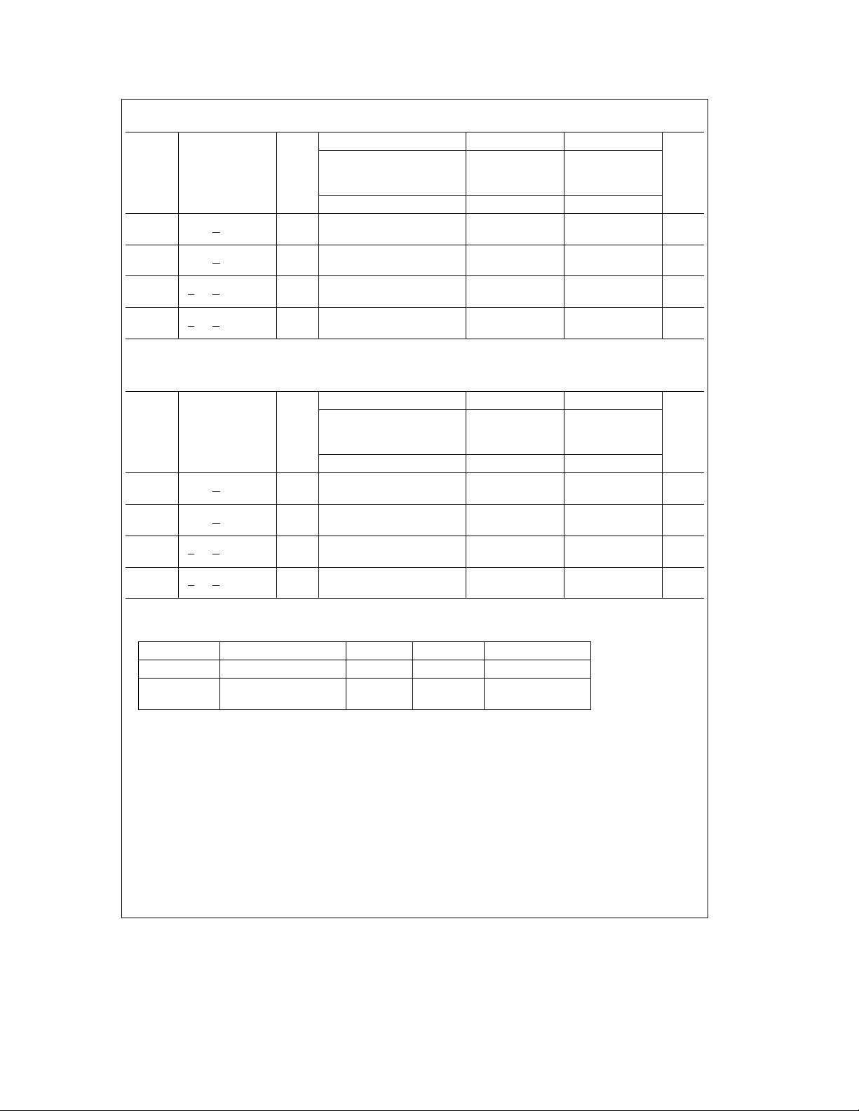
AC Electrical Characteristics
Symbol Parameter
t
PLH
t
PHL
t
PLH
t
PHL
*Voltage Range 3.3 is 3.3Vg0.3V
Voltage Range 5.0 is 5.0V
Propagation Delay 3.3 4.0 8.0 11.5 1.0 14.5 3.5 13.0
Anto O
n
Propagation Delay 3.3 3.0 7.0 10.0 1.0 12.5 2.5 11.0
A
to O
n
n
Propagation Delay 3.3 4.5 9.5 12.0 1.0 14.5 3.5 13.0
E
to O
n
n
Propagation Delay 3.3 4.0 8.0 10.0 1.0 12.5 3.0 11.0
Ento O
n
g
VCC* T
(V) C
5.0 3.0 6.5 8.5 1.0 11.0 2.5 9.5
5.0 2.5 5.5 7.5 1.0 10.0 2.0 8.5
5.0 3.5 7.0 8.5 1.0 11.0 3.0 10.0
5.0 2.5 6.0 7.5 1.0 10.0 2.5 8.5
0.5V
AC Electrical Characteristics
Symbol Parameter
t
PLH
t
PHL
t
PLH
t
PHL
*Voltage Range 5.0 is 5.0Vg0.5V
Propagation Delay
Anto O
n
Propagation Delay
A
to O
n
n
Propagation Delay
E
to O
n
n
Propagation Delay
Ento O
n
VCC* T
(V) C
5.0 1.5 6.0 8.5 1.0 12.0 1.5 9.5 ns
5.0 1.5 6.0 9.5 1.0 11.0 1.5 10.5 ns
5.0 2.5 7.0 10.0 1.0 12.5 2.0 11.0 ns
5.0 2.0 7.0 9.5 1.0 12.0 1.5 10.5 ns
74AC 54AC 74AC
A
ea
e
L
25§C
50 pF
eb
55§CT
T
A
a
125§Cto
to
e
C
50 pF C
L
eb
40§C
A
a
85§C Units
e
50 pF
L
Min Typ Max Min Max Min Max
74ACT 54ACT 74ACT
A
ea
e
L
25§C
50 pF
eb
55§CT
T
A
a
125§Cto
to
e
C
50 pF C
L
eb
40§C
A
a
85§C Units
e
50 pF
L
Min Typ Max Min Max Min Max
ns
ns
ns
ns
Capacitance
Symbol Parameter Typ Units Conditions
C
IN
C
PD
Input Capacitance 4.5 pF V
Power Dissipation
Capacitance
40.0 pF
5
e
OPEN
CC
e
V
5.0V
CC
Page 6
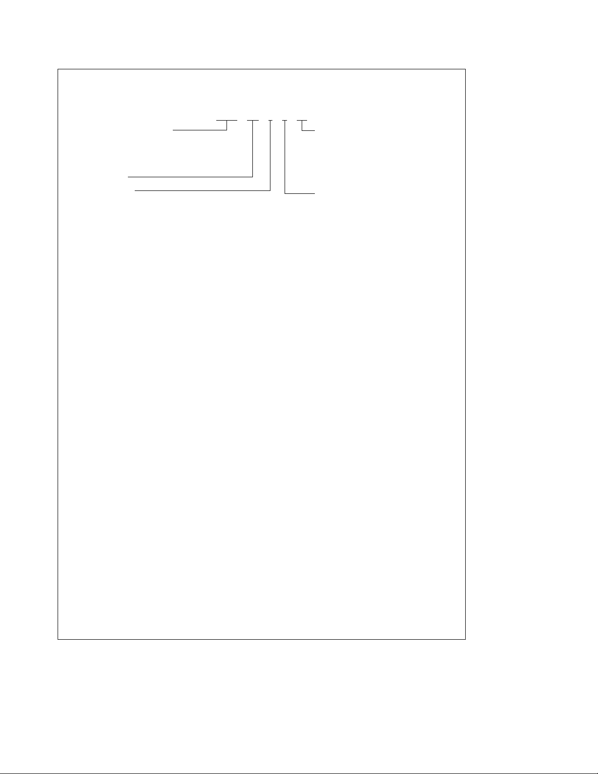
Ordering Information
The device number is used to form part of a simplified purchasing code where the package type and temperature range are
defined as follows:
74ACT 139 P C QR
Temperature Range Family Special Variations
e
74AC
Commercial XeDevices shipped in 13×reels
e
54AC
Military QReCommercial grade device
e
74ACT
54ACT
Device Type
Package Code
Commercial TTL-Compatible with burn-in
e
Military TTL-Compatible QBeMilitary grade device with
environmental and burn-in
processing shipped in tubes
e
Plastic DIP
P
e
Ceramic DIP
D
e
Flatpak
F
e
L
Leadless Ceramic Chip Carrier (LCC)
e
S
Small Outline (SOIC)
Temperature Range
e
Commercial (b40§Ctoa85§C)
C
e
Military (b55§Ctoa125§C)
M
6
Page 7

7
Page 8
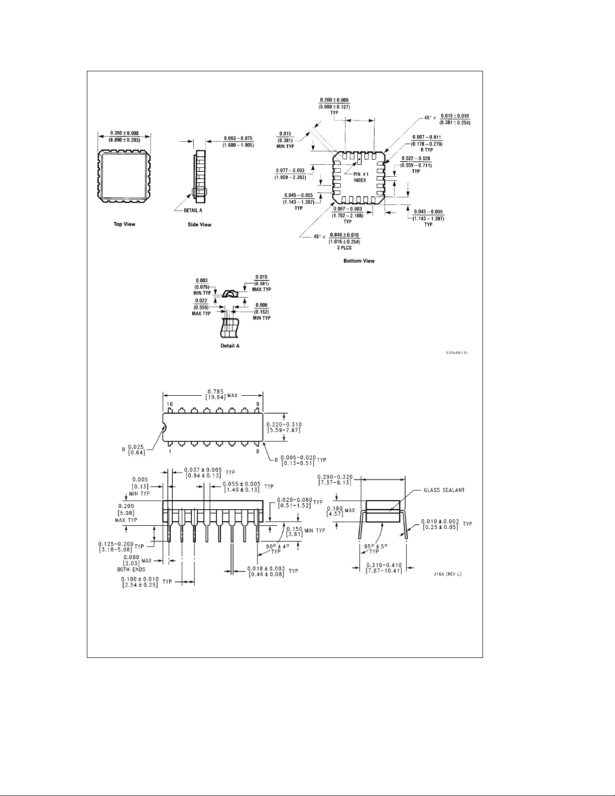
Physical Dimensions inches (millimeters)
20 Terminal Ceramic Leadless Chip Carrier (L)
NS Package Number E20A
16 Lead Ceramic Dual In-Line Package (D)
NS Package Number J16A
8
Page 9
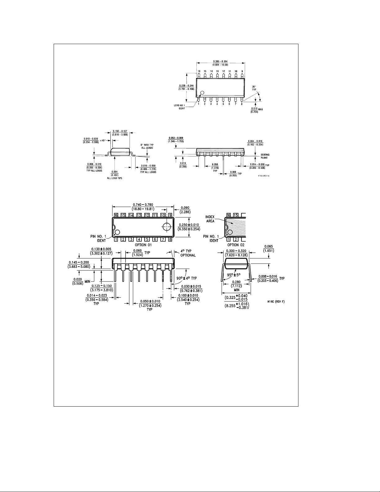
Physical Dimensions inches (millimeters) (Continued)
16 Lead Small Outline Integrated Circuit (S)
NS Package Number M16A
16 Lead Plastic Dual-In-Line Package (P)
NS Package Number N16E
9
Page 10
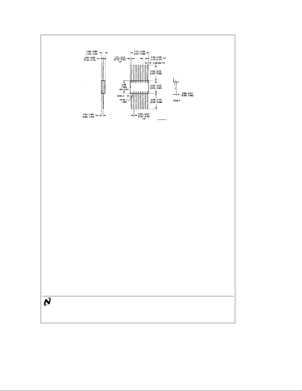
Physical Dimensions inches (millimeters) (Continued)
16 Lead Ceramic Flatpak (F)
NS Package Number W16A
54ACT/74ACT139 Dual 1-of-4 Decoder/Demultiplexer
#
LIFE SUPPORT POLICY
54AC/74AC139
NATIONAL’S PRODUCTS ARE NOT AUTHORIZED FOR USE AS CRITICAL COMPONENTS IN LIFE SUPPORT
DEVICES OR SYSTEMS WITHOUT THE EXPRESS WRITTEN APPROVAL OF THE PRESIDENT OF NATIONAL
SEMICONDUCTOR CORPORATION. As used herein:
1. Life support devices or systems are devices or 2. A critical component is any component of a life
systems which, (a) are intended for surgical implant support device or system whose failure to perform can
into the body, or (b) support or sustain life, and whose be reasonably expected to cause the failure of the life
failure to perform, when properly used in accordance support device or system, or to affect its safety or
with instructions for use provided in the labeling, can effectiveness.
be reasonably expected to result in a significant injury
to the user.
National Semiconductor National Semiconductor National Semiconductor National Semiconductor National Semiconductores National Semiconductor
Corporation GmbH Japan Ltd. Hong Kong Ltd. Do Brazil Ltda. (Australia) Pty, Ltd.
2900 Semiconductor Drive Livry-Gargan-Str. 10 Sumitomo Chemical 13th Floor, Straight Block, Rue Deputado Lacorda Franco Building 16
P.O. Box 58090 D-82256 F4urstenfeldbruck Engineering Center Ocean Centre, 5 Canton Rd. 120-3A Business Park Drive
Santa Clara, CA 95052-8090 Germany Bldg. 7F Tsimshatsui, Kowloon Sao Paulo-SP Monash Business Park
Tel: 1(800) 272-9959 Tel: (81-41) 35-0 1-7-1, Nakase, Mihama-Ku Hong Kong Brazil 05418-000 Nottinghill, Melbourne
TWX: (910) 339-9240 Telex: 527649 Chiba-City, Tel: (852) 2737-1600 Tel: (55-11) 212-5066 Victoria 3168 Australia
National does not assume any responsibility for use of any circuitry described, no circuit patent licenses are implied and National reserves the right at any time without notice to change said circuitry and specifications.
Fax: (81-41) 35-1 Ciba Prefecture 261 Fax: (852) 2736-9960 Telex: 391-1131931 NSBR BR Tel: (3) 558-9999
Tel: (043) 299-2300 Fax: (55-11) 212-1181 Fax: (3) 558-9998
Fax: (043) 299-2500
 Loading...