

Page 1
74ACT138
3 TO 8 LINE DECODER (INVERTING)
■ HIGH SPEED: t
■ LOWPOWERDISSIPATION:
=8µA (MAX.)at TA=25oC
I
CC
■ COMPATIBLEWITH TTL OUTPUTS
V
=2V(MIN),VIL= 0.8V (MAX)
IH
■ 50Ω TRANSMISSIONLINE DRIVING
=5 ns (TYP.) atVCC=5V
PD
CAPABILITY
■ SYMMETRICAL OUTPUT IMPEDANCE:
|I
|=IOL=24 mA (MIN)
OH
■ BALANCED PROPAGATION DELAYS:
t
≅ t
PLH
PHL
■ OPERATINGVOLTAGERANGE:
V
(OPR)= 4.5V to 5.5V
CC
■ PIN AND FUNCTION COMPATIBLE WITH
74SERIES138
■ IMPROVED LATCH-UP IMMUNITY
DESCRIPTION
The ACT138 is an advanced high-speed CMOS 3
TO 8 LINE DECODER (INVERTING) fabricated
with sub-micron silicon gate and double-layer
metal wiring C
2
MOS technology.
If the device is enabled, 3 binary select inputs (A,
B and C) determine which one of the outputs will
go low. If enable input G1 is held low or either
G2Aor G2G is held high, the decodingfunctionis
inhibitedand all the 8 outputs go to high.
B
(Plastic Package)
(Micro Package)
M
ORDERCODES:
74ACT138B
Three enable inputs are provided to ease
cascade connection and application of address
decodersfor memory systems.
It is ideal for low power applications mantaining
high speed operation similar to equivalent Bipolar
SchottkyTTL.
The device is designed to interface directly High
Speed CMOS systems with TTL, NMOS and
CMOSoutput voltage levels.
All inputs and outputs are equipped with
protectioncircuits against static discharge, giving
them 2KV ESD immunity and transient excess
voltage.
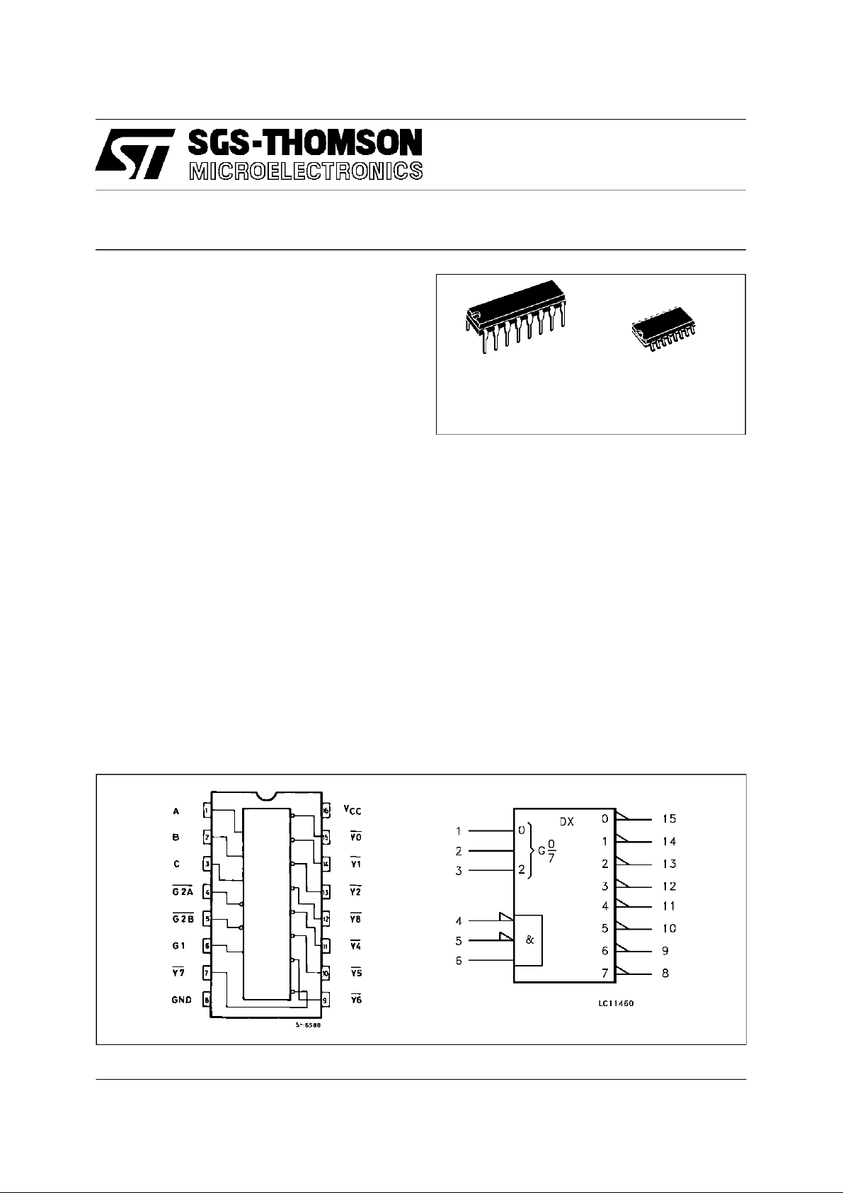
PINCONNECTION AND IEC LOGIC SYMBOLS
April 1997
1/8
Page 2
74ACT138
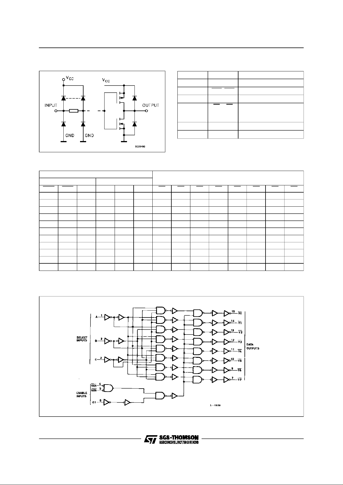
INPUTAND OUTPUTEQUIVALENTCIRCUIT
PIN DESCRIPTION
PI N No SYM B O L NAME A ND FUNCT I ON
1, 2, 3 A, B, C Address Inputs
4, 5 G2A, G2B Enable Inputs
6 G1 Enable Input
15, 14, 13,
12, 11, 10,
9, 7
8 GND Ground (0V)
16 V
Y0 to Y7 Outputs
CC
Positive Supply Voltage
TRUTH TABLE
INPUTS OUTPUTS
ENABLE SELEC T
G2B G2A G1 C B A Y0 Y1 Y2 Y3 Y4 Y5 Y6 Y7
XXLXXXHHHHHHHH
XHXXXXHHHHHHHH
HXXXXXHHHHHHHH
LLHLL LLHHHHHHH
LLHLLHHLHHHHHH
LLHLHLHHLHHHHH
LLHLHHHHHLHHHH
LLHHL LHHHHLHHH
LLHHLHHHHHHLHH
LLHHHLHHHHHHLH
LLHHHHHHHHHHHL
X:Don’t Care
LOGICDIAGRAMS
This logic diagram has not be used to estimate propagation delays
2/8
Page 3
74ACT138
ABSOLUTE MAXIMUMRATINGS
Symb o l Parame t er Val u e Uni t
V
V
V
I
I
OK
I
orI
I
CC
T
T
Absolute Maximum Ratings are those values beyond which damage to the device may occur. Functional operation under these condition is not implied.
RECOMMENDED OPERATINGCONDITIONS
Symbol Parameter Valu e Unit
V
V
V
T
dt/dv Input Rise and Fall Time V
1) VINfrom0.8V to2.0 V
Supply Voltage -0.5 to +7 V
CC
DC Input Voltage -0.5 to VCC+ 0.5 V
I
DC Output Voltage -0.5 to VCC+ 0.5 V
O
DC Input Diode Current ± 20 mA
IK
DC Output Diode Current ± 20 mA
DC Output Current ± 50 mA
O
DC VCCor Ground Current ± 400 mA
GND
Storage Temperature -65 to +150
stg
Lead Temperature (10 sec) 300
L
Supply Voltage 4.5 to 5.5 V
CC
Input Voltage 0 to V
I
Output Voltage 0 to V
O
Operating Temperature: -40to +85
op
= 4.5 to 5.5V (note 1) 8 ns/V
CC
CC
CC
o
C
o
C
V
V
o
C
3/8
Page 4

74ACT138
DC SPECIFICATIONS
Symbol Parameter Test Condit ions Value Unit
T
V
CC
(V)
High Level Input Voltage 4.5 VO= 0.1 V or
V
IH
5.5 2.0 1.5 2.0
Low Level Input Voltage 4.5 VO= 0.1 V or
V
IL
5.5 1.5 0.8 0.8
High Level Output
V
OH
Voltage
4.5
5.5 I
4.5 I
5.5 I
Low Level Output
V
OL
Voltage
4.5
5.5 I
4.5 I
5.5 I
Input Leakage Current
I
I
Max ICC/Input 5.5 VI=VCC-2.1 V 0.6 1.5 mA
I
CCT
Quiescent Supply
I
CC
5.5
5.5 VI=VCCor GND 8 80 µA
V
- 0.1 V
CC
- 0.1 V
V
CC
IO=-50 µA 4.4 4.49 4.4
(*)
=
V
I
V
IH
V
IL
(*)
V
I
V
IH
V
IL
=-50 µA 5.4 5.49 5.4
O
or
=-24 mA 3.86 3.76
O
=-24 mA 4.86 4.76
O
IO=50 µA 0.001 0.1 0.1
=
=50 mA 0.001 0.1 0.1
O
or
=24 mA 0.36 0.44
O
=24 mA 0.36 0.44
O
VI=VCCor GND ±0.1 ±1 µA
=25oC-40to85
A
Min. T yp . Max. Min. Max.
2.0 1.5 2.0
1.5 0.8 0.8
o
C
Current
Dynamic Output Current
I
OLD
OHD
(note 1, 2)
I
1) Maximum testduration 2ms, one output loaded at time
2) Incident wave switching is guaranteed on transmission lines with impedances as low as 50 Ω.
(*)All outputs loaded.
5.5 V
= 1.65 V max 75 mA
OLD
V
= 3.85 V min -75 mA
OHD
V
V
V
V
AC ELECTRICAL CHARACTERISTICS (CL= 50 pF, RL=500 Ω, Inputtr=tf=3ns)
Symbol Parame ter Test Conditi on Value Unit
t
Propagation Delay Time
PLH
t
A, B, C to Y
PHL
Propagation Delay Time
t
PLH
G1 to Y
t
PHL
Propagation Delay Time
t
PLH
t
G2A or G2B to Y
PHL
(*) Voltagerangeis5V± 0.5V
V
(V)
5.0
5.0
5.0
CC
(*)
(*)
(*)
T
=25oC-40to85
A
Min. T yp . Max. Min. Max.
5.0 10.0 11.0 ns
5.0 10.0 11.0 ns
5.5 10.0 11.0 ns
o
C
CAPACITIVE CHARACTERISTICS
Symbol Parameter Test Condit ions Value Unit
T
=25oC-40to85
A
Min. T yp . Max. Min. Max.
4
Input Capacitance
C
IN
Power Dissipation
C
PD
V
CC
(V)
5.0
5.0 25 pF
Capacitance (note 1)
1) CPDis defined as the value ofthe IC’s internal equivalent capacitance which is calculated from the operating current consumption without load. (Refer to
Test Circuit). Average operating current can be obtained by the following equation. I
(opr)= CPD• VCC•fIN+ICC/n (percircuit)
CC
o
C
pF
4/8
Page 5

74ACT138
WAVEFORM 1: PROPAGATION DELAYS FOR INVERTINGOUTPUTS (f=1MHz; 50% duty cycle)
WAVEFORM 2: PROPAGATION DELAYS FOR NON-INVERTING OUTPUTS (f=1MHz; 50%duty cycle)
5/8
Page 6

74ACT138
Plastic DIP16 (0.25) MECHANICAL DATA
DIM.
MIN. TYP. MAX. MIN. TYP. MAX.
a1 0.51 0.020
B 0.77 1.65 0.030 0.065
b 0.5 0.020
b1 0.25 0.010
D 20 0.787
E 8.5 0.335
e 2.54 0.100
e3 17.78 0.700
F 7.1 0.280
I 5.1 0.201
L 3.3 0.130
Z 1.27 0.050
mm inch
6/8
P001C
Page 7

SO16 MECHANICAL DATA
74ACT138
DIM.
MIN. TYP. MAX. MIN. TYP. MAX.
A 1.75 0.068
a1 0.1 0.2 0.004 0.007
a2 1.65 0.064
b 0.35 0.46 0.013 0.018
b1 0.19 0.25 0.007 0.010
C 0.5 0.019
c1 45 (typ.)
D 9.8 10 0.385 0.393
E 5.8 6.2 0.228 0.244
e 1.27 0.050
e3 8.89 0.350
F 3.8 4.0 0.149 0.157
G 4.6 5.3 0.181 0.208
L 0.5 1.27 0.019 0.050
M 0.62 0.024
S 8 (max.)
mm inch
P013H
7/8
Page 8

74ACT138
Information furnishedis believed to be accurate and reliable. However, SGS-THOMSON Microelectronics assumes no responsability for the
consequencesof use of such information nor for any infringement of patentsor other rights of third parties whichmay results from its use. No
licenseis granted byimplication or otherwise underany patentor patentrights ofSGS-THOMSONMicroelectronics. Specificationsmentioned
in this publicationare subject to change withoutnotice. This publication supersedes and replacesall information previously supplied.
SGS-THOMSONMicroelectronics productsarenot authorized for useascriticalcomponents in lifesupportdevices or systemswithoutexpress
writtenapproval of SGS-THOMSONMicroelectonics.
1997 SGS-THOMSONMicroelectronics- Printed in Italy - All Rights Reserved
Australia- Brazil - Canada- China- France- Germany - Hong Kong- Italy- Japan- Korea - Malaysia- Malta - Morocco - The Netherlands-
Singapore- Spain- Sweden- Switzerland - Taiwan- Thailand - United Kingdom - U.S.A
SGS-THOMSONMicroelectronics GROUP OF COMPANIES
.
8/8
 Loading...