

Datasheet 74ACT1284MTCX, 74ACT1284MTC, 74ACT1284MSAX, 74ACT1284MSA, 74ACT1284CW Datasheet (Fairchild Semiconductor)
...Page 1
© 1999 Fairchild Semiconductor Corporation DS011683 www.fairchildsemi.com
June 1996
Revised November 1999
74ACT1284 IEEE 1284 Transceiver
74ACT1284
IEEE 1284 Transceiver
General Description
The 74ACT1284 contains four non-inver ting bidirectional
buffers and three non-inverting buffers with open Drain outputs and high drive capability on the B Ports. It is intended
to provide a standard signaling method for a bi-direct ion
parallel peripheral in an Extended Capabi lities Port mode
(ECP).
The HD (active HIGH) input pin enables the B Ports to
switch from open Drain to a high drive totem pole o utput,
capable of sourcing 14 mA on all seven buffers. The D IR
input determines the d irection of data flow on the bidirectional buffers. DIR (active H IGH) enab les data f low from A
Ports to B Ports. DIR (activ e LOW ) enab les data flo w from
B Ports to A Por ts .
Features
■ TTL-compatible inputs
■ A Ports have standard 4 mA totem pole outputs
■ Typical input hysteresis of 0. 5V
■ B Port high drive source/sink capability of 14 mA
■ Bidirectional non-inverting buffers
■ Supports IEEE P1284 Level 1 and Level 2 signaling
standards for bidirectional parallel communications
between personal computers and printing peripherals
■ B Port outputs in H igh Impedance mode during power
down
■ Guarante ed 4000V minimum ESD protection
Ordering Code:
Device also available in Tape and Reel. Specify by appending suffix letter “X” to the ordering code.
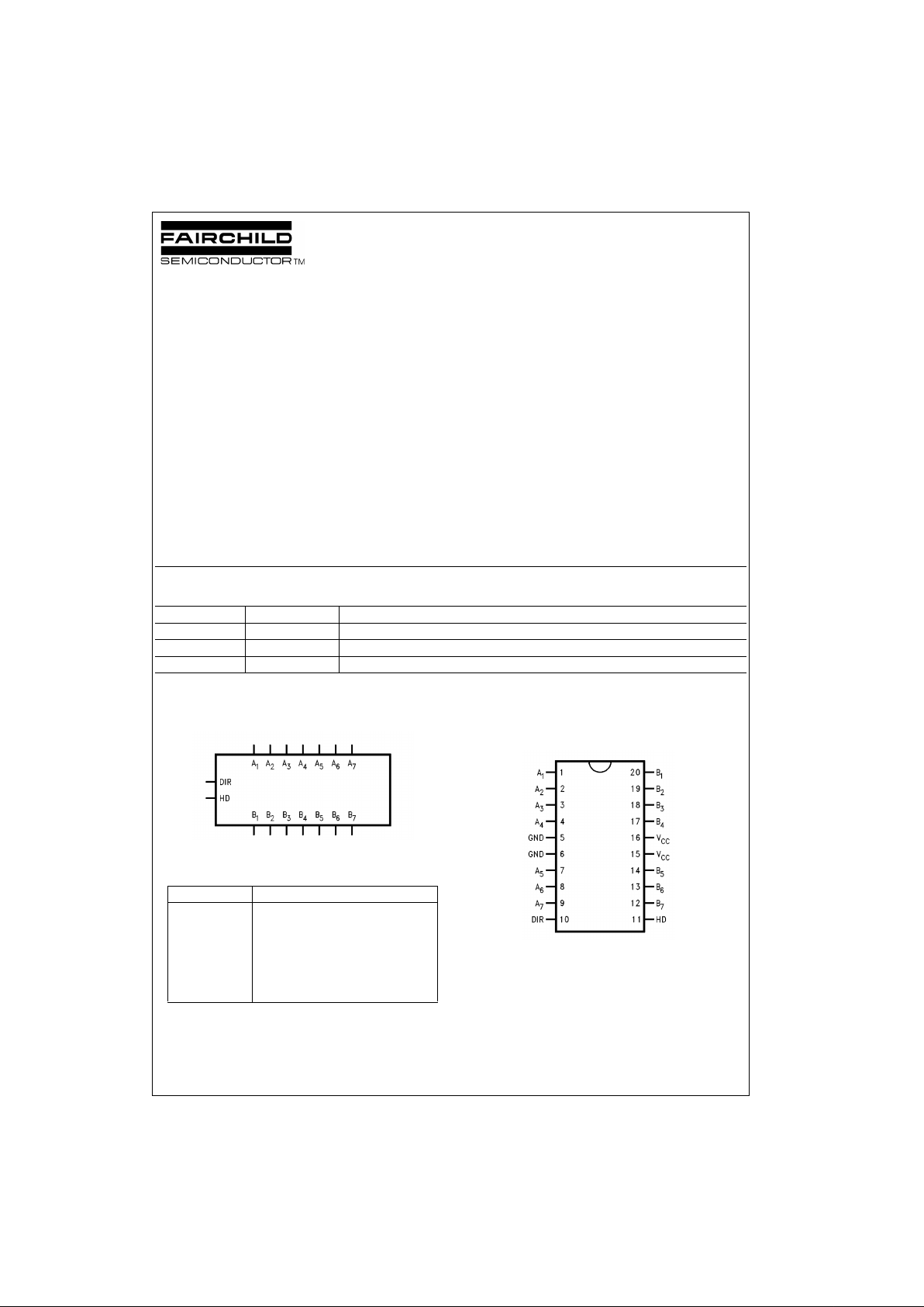
Logic Symbol
Pin Descriptions
Connection Diagram
FACT is a trademark of Fairchild Semiconductor Corporation.
Order Number Package Number Package Description
74ACT1284SC M20B 20-Lead Small Outline Integrated Circuit (SOIC), JEDEC MS-013, 0.300 Wide
74ACT1284MSA MSA20 20-Lead Shrink Small Outline Package (SSOP), EIAJ TYPE II, 5.3mm Wide
74ACT1284MTC MTC20 20-Lead Thin Shrink Small Outline Package (TSSOP), JEDEC MO-153, 4.4mm Wide
Pin Names Description
HD High Drive Enable input (Active HIGH)
DIR Direction Control Input
A
1
- A
4
Side A Inputs or Outputs
B
1
- B
4
Side B Inputs or Outputs
A
5
- A
7
Side A Inputs
B
5
- B
7
Side B Outputs
Page 2

www.fairchildsemi.com 2
74ACT1284
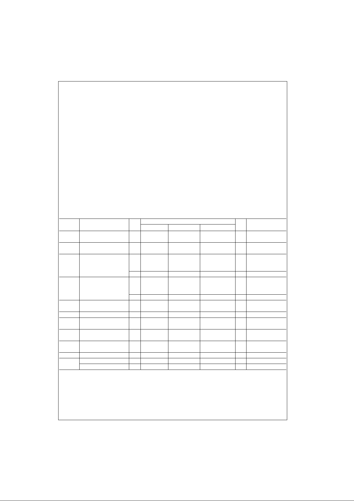
Truth Table
Note 1: B5 - B7 Open Drain Outputs
Note 2: B
1
- B7 Open Drain Outputs
Logic Diagram
Inputs
Outputs
DIR HD
LLB
1
- B4 Data to A1 - A4, and
A
5
- A7 Data to B5 - B7 (Note 1)
LHB
1
- B4 Data to A1 - A4, and
A
5
- A7 Data to B5 - B
7
HLA
1
- A7 Data to B1 - B7 (Note 2)
HHA
1
- A7 Data to B1 - B
7
Page 3
3 www.fairchildsemi.com
74ACT1284
Absolute Maximum Ratings(Note 3)
(Note 4)
Recommended Operating
Conditions
Note 3: Absolute max imum ratings are those values beyond which da m age
to the device may occu r. The databook spe cificatio ns shou ld be met, wit hout exception, to ensure that the system de sign is relia ble over its p ower
supply, temperature, and output/input loading variables. Fairchild does not
recommend operation of FACT circuits outside databook s pecifications.
Note 4: Either voltage lim it or c urrent limit is sufficient to protect inputs.
DC Electrical Characteristics
Note 5: All outputs loaded; thres holds on input associated with output unde r te s t .
Note 6: This parameter is guaranteed but not tested, characterized only: RD is the measure of the B-Side output impedance with the output in the HIGH
state.
Supply Voltage (VCC) −0.5V to +7.0V
DC Input Diode Current (I
IK
)
V
I
= −0.5V −20 mA
V
I
= VCC + 0.5V +20 mA
DC Input Voltage (V
I
) A Side −0.5V to VCC + 0.5V
DC Input Voltage (V
I
) B Side −2V to +7V
DC Output Diode Current (I
OK
)
V
O
= −0.5V −20 mA
V
O
= VCC + 0.5V +20 mA
DC Output Voltage (V
O
) A Side −0.5V to VCC + 0.5V
DC Output Voltage (V
O
) B Side −2V to +7V
DC Output Source
or Sink Current (I
O
) ± 50 mA
DC V
CC
or Ground Current
per Output Pin (I
CC
or I
GND
) ± 50 mA
Storage Temperature (T
STG
) −65°C to +150°C
Supply Voltage (V
CC
) 4.7V to 5.5V
Input Voltage (V
I
)0V to V
CC
Output Voltage (VO)0V to V
CC
Operating Temperature (TA) −40°C to +85°C
Symbol Parameter
V
CC
(V)
Guaranteed Limits
Units Conditions
TA = +25°CTA = 0°C to +70°CTA = −40°C to +85°C
V
IH
Minimum HIGH Level 4.7 2.0 2.0 2.0
V
Recognized
Input Voltage 5.5 2.0 2.0 2.0 High Signal
V
IL
Maximum LOW Level 4.7 0.8 0.8 0.8
V
Recognized
Input Voltage 5.5 0.8 0.8 0.8 Low Signal
V
OH
Minimum HIGH Level 4.7 4.5 4.5 4.5 I
OUT
= −50 µA (An)
Output Voltage VV
IN
= VIL or VIH (Note 5)
4.7 3.7 3.7 3.7 IOH = −4 mA (An)
4.7 2.4 2.4 2.4 V I
OH
= −14 mA (Bn)
V
OL
Maximum LOW Level 4.7 0.2 0.2 0.2 I
OUT
= 50 µA (An)
Output Voltage VVIN = VIL or VIH (Note 5)
4.7 0.4 0.4 0.4 I
OH
= 4 mA (An)
VI
OH
= 14 mA (Bn)
I
IN
Maximum Input
5.5 ±0.1 ±1.0 µA
VI = VCC, GND
Leakage Current (DIR, A5, A6, A7, HD)
I
CCT
Maximum ICC/Input 5.5 1.5 1.5 mA VI = VCC − 2.1V
I
CC
Maximum Quiescent
5.5 400 400 500 µAVIN = VCC or GND
Supply Current
I
OZ
Maximum Output
5.5 ±20 ±20 ±20 µAVO = VCC, GND
Leakage Current
I
OFF
Maximum B-Side Power Down
0.0 100 100 100 µAV
OUT
= 5.25V
Leakage Current
∆
VT
Input Hysteresis 5.0 0.4 0.4 0.35 V VT + − VT−
R
D
Maximum Output Impedance 5.0 22 22 24 Ω Bn (Note 6)
Minimum Output Impedance 5.0 8 8 6 Ω Bn (Note 6)
Page 4

www.fairchildsemi.com 4
74ACT1284
AC Electrical Characteristics
Note 7: Open Drain
Note 8: This parameter is guaranteed but not tested, characterized only.
Note: Pulse Generator for all pulses; Rate
≤ 1.0 MHz; A
O
≤ 50Ω; tf ≤ 2.5 ns, tr ≤ 2.5 ns.
Capacitance
Symbol Parameter
T
A
= +25°CTA = 0°C to +70°CTA = −40°C to +85°C
Units
Figure
Number
V
CC
= 4.7V − 5.5V VCC = 4.7V − 5.5V VCC = 4.7V − 5.5V
Min Max Min Max Min Max
t
PHL
A1- A7 to B1 - B
7
2.0 20.0 2.0 20.0 2.0 24.0 ns Figure 1
t
PLH
A1- A7 to B1 - B
7
2.0 20.0 2.0 20.0 2.0 24.0 ns Figure 2
t
PHL
B1 - B4 to A1 - A
4
2.0 20.0 2.0 20.0 2.0 24.0 ns Figure 3
t
PLH
B1 - B4 to A1 - A
4
2.0 20.0 2.0 20.0 2.0 24.0 ns Figure 3
t
pEnable
Output Enable Time
2.0 20.0 2.0 20.0 2.0 24.0 ns Figure 2
HD to B1 - B
7
t
pDisable
Output Disable Time
2.0 20.0 2.0 20.0 2.0 24.0 ns Figure 2
HD to B
1
- B
7
t
SKEW
Output Slew Rate
0.05 0.40 0.05 0.40 0.05 0.40 V/ns
Figure 1
t
PLH
B1 - B
7
Figure 2
t
PHL
tr, t
f
t
RISE
and t
FALL
120 120 120 ns
Figure 4
B
1
- B7 (Note 7) (Note 8)
Symbol Parameter Typ Units Conditions
C
IN
Input Capacitance 4.0 pF VCC = OPEN (HD, DIR A5 - A7)
C
I/O
I/O Pin Capacitance 12.0 pF VCC = 5.0V
Page 5

5 www.fairchildsemi.com
74ACT1284
AC Loading and Waveforms
t
SLEW
measures between 10% to 90% on the t
PHL
Transition
FIGURE 1. A to B Direction Test Load and Waveforms
t
SLEW
measures between 10% to 90% on the t
PLH
Transition
FIGURE 2. B Output Test Load and Waveforms
FIGURE 3. B to A D irection Test Load and Waveforms for Outputs A
1
- A
4
FIGURE 4. A to B Direction Test Load and Waveforms for Open Drain B1 - B
7
Page 6

www.fairchildsemi.com 6
74ACT1284
Physical Dimensions inches (millimeters) unless otherwise noted
20-Lead Small Outline Integrated Circuit (SOIC), JEDEC MS-013, 0.300 Wide
Package Number M20B
20-Lead Shrink Small Outline Package (SSOP), EIAJ TYPE II, 5.3mm Wide
Package Number MSA20
Page 7

Physical Dimensions inches (millimeters) unless otherwise noted (Continued)
7 www.fairchildsemi.com
74ACT1284 IEEE 1284 Transceiver
Physical Dimensions inches (millimeters) unless otherwise noted (Continued)
20-Lead Thin Shrink Sm all Ou tline Pa ck age (TS SO P), JE DE C MO-153, 4.4mm Wide
Package Number MTC20
Fairchild does not assume any responsibility for use of any circuitry described , no circuit patent licenses are implied and
Fairchild reserves the right at any time without notice to change said circuitry and specifications.
LIFE SUPPORT POLICY
FAIRCHILD’S PRODUCTS ARE NOT AUTHORIZED FOR USE AS CRITICAL COMPONENTS IN LIFE SUPPORT
DEVICES OR SYSTEMS WITHOUT THE EXPRESS WRITTEN APPROVAL OF THE PRESIDENT OF FAIRCHILD
SEMICONDUCTOR CORPORATION. As used herein:
1. Life support devices or systems are dev ic es or syste ms
which, (a) are intended for surgical implant into the
body, or (b) support or sustain life, and (c) whose failure
to perform when properly used in accordance with
instructions for use provide d in the labe l ing, can be re asonably expected to result in a significant injury to the
user.
2. A critical compo nent in any com ponen t of a life s upp ort
device or system whose failure to perform can be reasonably expected to cause the failure of the l ife s upport
device or system, or to affect its safety or effectiveness.
www.fairchildsemi.com
 Loading...